DDR3以MT41J128M8 1GB
MEMORY存储芯片MT41J64M16JT-125G中文规格书
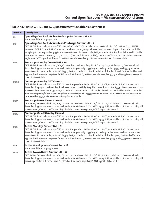
Active Power-Down Current (AL = 0) CKE: LOW; External clock: on; tCK, CL: see the previous table; BL: 8;1 AL: 0; CS_n: stable at 1; Command, address, bank group address, bank address inputs: stable at 1; Data I/O: VDDQ; DM_n: stable at 1; Bank activity: all banks open; Output buffer and RTT: Enabled in mode registers;2 ODT signal: stable at 0
Precharge Standby ODT Current CKE: HIGH; External clock: on; tCK, CL: see the previous table; BL: 8;1 AL: 0; CS_n: stable at 1; Command, address, bank gropup address, bank address inputs: partially toggling according to the IDD2NT Measurement-Loop Pattern table; Data I/O: VSSQ; DM_n: stable at 1; Bank activity: all banks closed; Output buffer and RTT: enabled in mode registers;2 ODT signal: toggling according to the IDD2NT Measurement-Loop Pattern table; Pattern details: see the IDD2NT Measurement-Loop Pattern table
MT41K256M16HA-125E

• TC of 0°C to +95°C – 64ms, 8192-cycle refresh at 0°C to +85°C – 32ms at +85°C to +95°C
1KB
512 Meg x 8 64 Meg x 8 x 8 banks
8K 64K (A[15:0])
8 (BA[2:0]) 1K (A[9:0])
1KB
256 Meg x 16 32 Meg x 16 x 8 banks
8K 32K (A[14:0])
8 (BA[2:0]) 1K (A[9:0])
PDF: 09005aef84780270 4Gb_DDR3L_SDRAM.pdf - Rev. H 4/13 EN
3
Micron Technology, Inc. reserves the right to change products or specifications without notice. © 2011 Micron Technology, Inc. All rights reserved.
1.35V DDR3L SDRAM
MT41K1G4 – 128 Meg x 4 x 8 banks MT41K512M8 – 64 Meg x 8 x 8 banks MT41K256M16 – 32 Meg x 16 x 8 banks
4Gb: x4, x8, x16 DDR3L SDRAM Description
A14
MT41K256M16HA-125IT_E
DDR3L SDRAMMT41K1G4 – 128 Meg x 4 x 8 banksMT41K512M8 – 64 Meg x 8 x 8 banks MT41K256M16 – 32 Meg x 16 x 8 banksDescriptionDDR3L SDRAM (1.35V) is a low voltage version of the DDR3 (1.5V) SDRAM. Refer to DDR3 (1.5V) SDRAM (Die Rev :E) data sheet specifications when running in 1.5V compatible mode.Features•V DD = V DDQ = 1.35V (1.283–1.45V)•Backward compatible to V DD = V DDQ = 1.5V ±0.075V –Supports DDR3L devices to be backward com-patible in 1.5V applications•Differential bidirectional data strobe•8n-bit prefetch architecture•Differential clock inputs (CK, CK#)•8 internal banks•Nominal and dynamic on-die termination (ODT) for data, strobe, and mask signals •Programmable CAS (READ) latency (CL)•Programmable posted CAS additive latency (AL)•Programmable CAS (WRITE) latency (CWL)•Fixed burst length (BL) of 8 and burst chop (BC) of 4 (via the mode register set [MRS])•Selectable BC4 or BL8 on-the-fly (OTF)•Self refresh mode•T C of 105°C–64ms, 8192-cycle refresh up to 85°C–32ms, 8192-cycle refresh at >85°C to 95°C–16ms, 8192-cycle refresh at >95°C to 105°C •Self refresh temperature (SRT)•Automatic self refresh (ASR)•Write leveling•Multipurpose register•Output driver calibrationOptions Marking •Configuration– 1 Gig x 41G4–512 Meg x 8512M8–256 Meg x 16256M16•FBGA package (Pb-free) – x4, x8–78-ball (9mm x 10.5mm) Rev. E RH–78-ball (7.5mm x 10.6mm) Rev. N RG–78-ball (8mm x 10.5mm) Rev. P DA •FBGA package (Pb-free) – x16–96-ball (9mm x 14mm) Rev. E HA–96-ball (7.5mm x 13.5mm) Rev. N LY–96-ball (8mm x 14mm) Rev. P TW •Timing – cycle time–938ps @ CL = 14 (DDR3-2133)-093– 1.07ns @ CL = 13 (DDR3-1866)-107– 1.25ns @ CL = 11 (DDR3-1600)-125•Operating temperature–Commercial (0°C T C +95°C)None–Industrial (–40°C T C +95°C)IT–Automotive (–40°C T C +105°C)AT •Revision:E/:N/:PTable 1: Key Timing ParametersNotes: 1.Backward compatible to 1600, CL = 11 (-125).2.Backward compatible to 1866, CL = 13 (-107).4Gb: x4, x8, x16 DDR3L SDRAMDescription质量等级领域:宇航级IC、特军级IC、超军级IC、普军级IC、禁运IC、工业级IC,军级二三极管,功率管等;应用领域:航空航天、船舶、汽车电子、军用计算机、铁路、医疗电子、通信网络、电力工业以及大型工业设备祝您:工作顺利,生活愉快!以深圳市美光存储技术有限公司提供的参数为例,以下为MT41K256M16HA-125IT_E的详细参数,仅供参考DDR3L 1.35V Slew Rate Definitions for Differential Input SignalsInput slew rate for differential signals (CK, CK# and DQS, DQS#) are defined and meas-ured, as shown in Table 31 and Figure 22. The nominal slew rate for a rising signal is defined as the slew rate between V IL,diff,max and V IH,diff,min . The nominal slew rate for a falling signal is defined as the slew rate between V IH,diff,min and V IL,diff,max .Table 31: DDR3L 1.35V Differential Input Slew Rate DefinitionFigure 22: DDR3L 1.35V Nominal Differential Input Slew Rate Definition for DQS, DQS# and CK, CK#ǻTR ǻTF diffV IH,diff,minV IL,diff,maxD i f f e r e n t i a l i n p u t v o l t a g e (D Q S , D Q S #; C K , C K #)4Gb: x4, x8, x16 DDR3L SDRAM Electrical Specifications – DC and ACODT CharacteristicsThe ODT effective resistance R TT is defined by MR1[9, 6, and 2]. ODT is applied to the DQ, DM, DQS, DQS#, and TDQS, TDQS# balls (x8 devices only). The ODT target values and a functional representation are listed in Table 32 and Table 33 (page 61). The indi-vidual pull-up and pull-down resistors (R TT(PU) and R TT(PD)) are defined as follows:•R TT(PU) = (V DDQ - V OUT )/|I OUT |, under the condition that R TT(PD) is turned off •R TT(PD) = (V OUT )/|I OUT |, under the condition that R TT(PU) is turned offFigure 23: ODT Levels and I-V CharacteristicsChip in termination modeDDQDQ V SSQ - I PUV OUTTable 32: On-Die Termination DC Electrical Characteristics1.35V ODT ResistorsTable 33 provides an overview of the ODT DC electrical characteristics. The values pro-vided are not specification requirements; however, they can be used as design guide-lines to indicate what R TT is targeted to provide:•R TT 120ȍ is made up of R TT120(PD240) and R TT120(PU240)•R TT 60ȍ is made up of R TT60(PD120) and R TT60(PU120)•R TT 40ȍ is made up of R TT40(PD80) and R TT40(PU80)•R TT 30ȍ is made up of R TT30(PD60) and R TT30(PU60)•R TT 20ȍ is made up of R TT20(PD40) and R TT20(PU40)Table 33: 1.35V R TT Effective Impedance。
MEMORY存储芯片MT41K128M16JT-125 IT中文规格书
–V DD and V DDQ are driven from a single-power converter output and applyV DD /V DDQ without any slope reversal before or at the same time as V TT andV REFCA .–The voltage levels on all balls other than V DD , V DDQ , V SS , and V SSQ must be lessthan or equal to V DDQ and V DD on one side and must be greater than or equalto V SSQ and V SS on the other side.–V TT is limited to 0.76V MAX when the power ramp is complete.–V REFCA tracks V DD /2.•Condition B:–Apply V PP without any slope reversal before or at the same time as V DD .–Apply V DD without any slope reversal before or at the same time as V DDQ .–Apply V DDQ without any slope reversal before or at the same time as V TT andV REFCA .–The voltage levels on all pins other than V PP , V DD , V DDQ , V SS , and V SSQ must beless than or equal to V DDQ and V DD on one side and must be larger than orequal to V SSQ and V SS on the other side.2.After RESET_n is de-asserted, wait for a minimum of 500μs, but no longer than 3seconds, before allowing CKE to be registered HIGH at clock edge Td. During thistime, the device will start internal state initialization; this will be done independ-ently of external clocks. A reasonable attempt was made in the design to power upwith the following default MR settings: gear-down mode (MR3 A[3]): 0 = 1/2 rate;per-DRAM addressability (MR3 A[4]): 0 = disable; maximum power-down (MR4A[1]): 0 = disable; CS to command/address latency (MR4 A[8:6]): 000 = disable; CAparity latency mode (MR5 A[2:0]): 000 = disable. However, it should be assumedthat at power up the MR settings are undefined and should be programmed asshown below.3.Clocks (CK_t, CK_c) need to be started and stabilized for at least 10ns or 5 t CK(whichever is larger) before CKE is registered HIGH at clock edge Td. Because CKEis a synchronous signal, the corresponding setup time to clock (t IS) must be met.Also, a DESELECT command must be registered (with t IS setup time to clock) atclock edge Td. After the CKE is registered HIGH after RESET, CKE needs to be con-tinuously registered HIGH until the initialization sequence is finished, includingexpiration of t DLLK and t ZQinit.4.The device keeps its ODT in High-Z state as long as RESET_n is asserted. Further,the SDRAM keeps its ODT in High-Z state after RESET_n de-assertion until CKE isregistered HIGH. The ODT input signal may be in an undefined state until t IS be-fore CKE is registered HIGH. When CKE is registered HIGH, the ODT input signalmay be statically held either LOW or HIGH. If R TT(NOM) is to be enabled in MR1,the ODT input signal must be statically held LOW. In all cases, the ODT input sig-nal remains static until the power-up initialization sequence is finished, includingthe expiration of t DLLK and t ZQinit.5.After CKE is registered HIGH, wait a minimum of RESET CKE EXIT time, t XPR, be-fore issuing the first MRS command to load mode register (t XPR = MAX (t XS, 5 ×t CK).6.Issue MRS command to load MR3 with all application settings, wait t MRD.7.Issue MRS command to load MR6 with all application settings, wait t MRD.8.Issue MRS command to load MR5 with all application settings, wait t MRD.9.Issue MRS command to load MR4 with all application settings, wait t MRD.10.Issue MRS command to load MR2 with all application settings, wait t MRD.11.Issue MRS command to load MR1 with all application settings, wait t MRD.8Gb: x4, x8, x16 DDR4 SDRAM RESET and Initialization ProcedureFigure 38: MPR READ-to-WRITE TimingT0T1T2DQ DQS_t,DQS_cTa0Ta1Ta2Ta3Ta4Ta5Ta6Tb0Tb1Tb2Command Address CKECK_tCK_cDon’t CareNotes: 1.Address setting:A[1:0] = 00b (data burst order is fixed starting at nibble, always 00b here)A2 = 0b (for BL = 8, burst order is fixed at 0, 1, 2, 3, 4, 5, 6, 7)BA1 and BA0 indicate the MPR locationA10 and other address pins are "Don’t Care," including BG1 and BG0. A12 is "Don’tCare" when MR0 A[1:0] = 00 and must be 1b when MR0 A[1:0] = 012.Address setting:BA1 and BA0 indicate the MPR locationA[7:0] = data for MPRBA1 and BA0 indicate the MPR locationA10 and other address pins are "Don’t Care"3.Parity latency (PL) is added to data output delay when CA parity latency mode is ena-bled.MPR WritesMPR access mode allows 8-bit writes to the MPR Page 0 using the address bus A[7:0].Data bus inversion (DBI) is not allowed during MPR WRITE operation. The DRAM willmaintain the new written values unless re-initialized or there is power loss.The following steps are required to use the MPR to write to mode register MPR Page 0.1.The DLL must be locked if enabled.2.Precharge all; wait until t RP is satisfied.3.MRS command to MR3[2] = 1 (enable MPR data flow) and MR3[1:0] = 00 (MPRPage 0); writes to 01, 10, and 11 are not allowed.4.t MRD and t MOD must be satisfied.5.Redirect all subsequent WRITE commands to specific MPR x location.6.Issue WR or WRA command:a.BA1 and BA0 indicate MPR x location1.00 = MPR02.01 = MPR13.10 = MPR24.11 = MPR3b.A[7:0] = data for MPR Page 0, mapped A[7:0] to UI[7:0].8Gb: x4, x8, x16 DDR4 SDRAM Multipurpose Register。
ARTIX-7 FPGA 核心板 用户手册说明书

ARTIX-7 FPGA核心板用户手册AC7A200REV 1.0版芯驿电子科技(上海)有限公司黑金动力社区目录(一)简介 (3)(二)FPGA (4)(三)有源差分晶振 (6)(四)DDR3 (8)(五)QSPI Flash (12)(六)LED灯 (13)(七)JTAG接口 (15)(八)电源接口 (15)(九)扩展接口 (16)(十)电源 (24)(十一)结构图 (27)(一)简介AC7A200(核心板型号,下同)核心板,是基于XILINX公司的ARTIX-7系列200T 的XC7A200T-2FBG484I这款芯片开发的高性能核心板,具有高速,高带宽,高容量等特点,适合高速数据通信,视频图像处理,高速数据采集等方面使用。
这款核心板使用了2片MICRON公司的MT41J256M16HA-125这款DDR3芯片,每片DDR的容量为4Gbit;2片DDR芯片组合成32bit的数据总线宽度,FPGA和DDR3之间的读写数据带宽高达25Gb;这样的配置,可以满足高带宽的数据处理的需求。
这款核心板扩展出180个3.3V电平标准普通IO口,15个1.5V电平标准的普通IO口,还有4对GTP高速RX/TX差分信号。
对于需要大量IO的用户,此核心板将是不错的选择。
而且,FPGA芯片到接口之间走线做了等长和差分处理,并且核心板尺寸仅为60*60(mm),对于二次开发来说非常适合。
AC7A200核心板正面图AC7A200核心板背面图(二)FPGA前面已经介绍过了,我们所使用的FPGA型号为XC7A200T-2FBG484I,属于Xilinx公司Artix-7系列的产品,速度等级为2,温度等级为工业级。
此型号为FBG484封装,484个引脚。
Xilinx ARTIX-7 FPGA的芯片命名规则如下:图2-2-1为开发板所用的FPGA芯片实物图。
图2-2-1 FPGA芯片实物FPGA供电系统Artix-7 FPGA电源有V CCINT, V CCBRAM, V CCAUX, V CCO, V MGTAVCC和V MGTAVTT。
MT41K512M16VRN-107IT_P

TwinDie 1.35V DDR3L SDRAMMT41K512M16 – 64 Meg x 16 x 8 Banks DescriptionThe 8Gb (TwinDie) DDR3L SDRAM (1.35V) uses twoMicron 4Gb DDR3L SDRAM x8 die for a 2 byte x16 de-vice in one package. Refer to Micron’s 4Gb DDR3L SDRAM data sheet (x8 option) for specifications not included in this document, specifications for base part number MT41K512M8 correlate to TwinDie manufac-turing base part number MT41K512M16.Features•Uses two x8, 4Gb Micron die to make one x16 pack-age–Single rank TwinDie–One external ZQ ball and one internal ZQ con-nected to V SSQ through an embedded serial resis-tor•V DD = V DDQ = 1.35V (1.283–1.45V)•Backward compatible to V DD = V DDQ = 1.5V ±0.075V •Differential bidirectional data strobe •8n -bit prefetch architecture•Differential clock inputs (CK, CK#)•8 internal banks•Nominal and dynamic on-die termination (ODT)for data, strobe, and mask signals•Programmable CAS (READ) latency (CL)•Programmable posted CAS additive latency (AL)•Programmable CAS (WRITE) latency (CWL)•Fixed burst length (BL) of 8 and burst chop (BC) of 4(via the mode register set [MRS])•Selectable BC4 or BL8 on-the-fly (OTF)•Self refresh mode •T C of –40°C to +95°C–64ms, 8192-cycle refresh at –40°C to +85°C –32ms at +85°C to +95°C •Self refresh temperature (SRT)•Automatic self refresh (ASR)•Write leveling•Multipurpose register •Output driver calibration OptionsMarking•Configuration –512 Meg x 16512M16•TFBGA package (Pb-free) – x16–96-ball (8mm x 14mm) - SAC302VRN –96-ball (8mm x 14mm) - SACQ VRP •Timing – cycle time– 1.07ns @ CL = 13 (DDR3-1866)-107•Self refresh –StandardNone •Operating temperature–Industrial (–40°C ≤ T C ≤ +95°C)IT •Revision:PNotes:1.Not all options listed can be combined todefine an offered product. Use the part cat-alog search on for available offer-ings.2.For recommendation on PCB vs. componentpad dimension, see CSN-33: Micron BGA Manufacturer’s User Guide on .Table 1: Key Timing ParametersTable 2: AddressingFigure 1: DDR3L Part NumbersExample Part Number: MT41K512M16xxx-107 IT:PNote:1.Not all options listed can be combined to define an offered product. Use the part catalog search on for available offerings.8Gb: x16 TwinDie DDR3L SDRAMDescription质量等级领域:宇航级IC 、特军级IC 、超军级IC 、普军级IC 、禁运IC 、工业级IC ,军级二三极管,功率管等;应用领域:航空航天、船舶、汽车电子、军用计算机、铁路、医疗电子、通信网络、电力工业以及大型工业设备祝您:工作顺利,生活愉快!以深圳市美光存储技术有限公司提供的参数为例,以下为MT41K512M16VRN-107IT_P的详细参数,仅供参考Electrical SpecificationsAbsolute RatingsStresses greater than those listed may cause permanent damage to the device. This is a stress rating only, and functional operation of the device at these or any other condi-tions outside those indicated in the operational sections of this specification is not im-plied. Exposure to absolute maximum rating conditions for extended periods may ad-versely affect reliability.Table 6: Absolute Maximum Ratings8Gb: x16 TwinDie DDR3L SDRAMElectrical Specifications。
镁光16GB DDR3 1600MHZ服务器内存条jsf36c2gx72pz
DDR3 SDRAM RDIMMMT36JSF2G72PZ – 16GB Features•DDR3 functionality and operations supported as defined in the component data sheet•240-pin, registered dual in-line memory module (RDIMM)•Fast data transfer rates: PC3-14900, PC3-12800,PC3-10600, PC3-8500, or PC3-6400•16GB (2 Gig x 72)•V DD = 1.5V ±0.075V •V DDSPD = 3.0–3.6V•Supports ECC error detection and correction•Nominal and dynamic on-die termination (ODT) for data and strobe signals •Dual-rank•8 internal device banks•Fixed burst chop (BC) of 4 and burst length (BL) of 8via the mode register set (MRS)•On-board I 2C temperature sensor with integrated serial presence-detect (SPD) EEPROM •Gold edge contacts •Halogen-free •Fly-by topology•Terminated control, command, and address bus Figure 1: 240-Pin RDIMM (R/C J1)Figure 2: 240-Pin RDIMM (R/C E2)OptionsMarking•Operating temperature–Commercial (0°C ≤ T A ≤ 70°C)None •Package–240-pin DIMM (halogen-free)Z •Frequency/CAS latency– 1.07ns @ CL = 13 (DDR3-1866)-1G9– 1.25ns @ CL = 11 (DDR3-1600)-1G6– 1.5ns @ CL = 9 (DDR3-1333)-1G4– 1.87ns @ CL = 7 (DDR3-1066)-1G1Table 1: Key Timing ParametersTable 2: AddressingTable 3: Part Numbers and Timing Parameters – 16GB Modules1Notes: 1.The data sheet for the base device can be found on Micron’s web site.2.All part numbers end with a two-place code (not shown) that designates component and PCB revisions.Consult factory for current revision codes. Example: MT36JSF2G72PZ-1G4N1.Pin Assignments Table 4: Pin AssignmentsPin DescriptionsThe pin description table below is a comprehensive list of all possible pins for all DDR3modules. All pins listed may not be supported on this module. See Pin Assignments forinformation specific to this module.Table 5: Pin DescriptionsTable 5: Pin Descriptions (Continued)DQ MapsTable 6: Component-to-Module DQ Map (R/C J1), FrontTable 6: Component-to-Module DQ Map (R/C J1), Front (Continued)Table 7: Component-to-Module DQ Map (R/C J1), BackTable 7: Component-to-Module DQ Map (R/C J1), Back (Continued)Table 8: Component-to-Module DQ Map (R/C E2), FrontTable 9: Component-to-Module DQ Map (R/C E2), BackFunctional Block DiagramsFigure 3: Functional Block Diagram (R/C J1)V REFCAV SSV DD V DDSPDV TT V REFDQClock, control, command, and address line terminations:Rank 0: U1–U5, U8–U20 Rank 1: U21–U38RODT[1:0], TTDDNote:1.The ZQ ball on each DDR3 component is connected to an external 240Ω ±1% resistorthat is tied to ground. It is used for the calibration of the component’s ODT and output driver.Figure 4: Functional Block Diagram (R/C E2)V V V V V TT V Clock, control, command, and address line terminations:Rank 0: U1–U5, U12–U16, U21–U24, U31–U34 Rank 1: U8–U11, U17–U20, U26–U30, U35–U39RODT[1:0], R DDNote:1.The ZQ ball on each DDR3 component is connected to an external 240Ω ±1% resistorthat is tied to ground. It is used for the calibration of the component’s ODT and output driver.General DescriptionDDR3 SDRAM modules are high-speed, CMOS dynamic random access memory mod-ules that use internally configured 8-bank DDR3 SDRAM devices. DDR3 SDRAM mod-ules use DDR architecture to achieve high-speed operation. DDR3 architecture is essen-tially an 8n -prefetch architecture with an interface designed to transfer two data words per clock cycle at the I/O pins. A single read or write access for the DDR3 SDRAM mod-ule effectively consists of a single 8n -bit-wide, one-clock-cycle data transfer at the inter-nal DRAM core and eight corresponding n -bit-wide, one-half-clock-cycle data transfers at the I/O pins.DDR3 modules use two sets of differential signals: DQS, DQS# to capture data and CK and CK# to capture commands, addresses, and control signals. Differential clocks and data strobes ensure exceptional noise immunity for these signals and provide precise crossing points to capture input signals.Fly-By TopologyDDR3 modules use faster clock speeds than earlier DDR technologies, making signal quality more important than ever. For improved signal quality, the clock, control, com-mand, and address buses have been routed in a fly-by topology, where each clock, con-trol, command, and address pin on each DRAM is connected to a single trace and ter-minated (rather than a tree structure, where the termination is off the module near the connector). Inherent to fly-by topology, the timing skew between the clock and DQS sig-nals can be easily accounted for by using the write-leveling feature of DDR3.Registering Clock Driver OperationRegistered DDR3 SDRAM modules use a registering clock driver device consisting of a register and a phase-lock loop (PLL). The device complies with the JEDEC standard "Definition of the SSTE32882 Registering Clock Driver with Parity and Quad Chip Se-lects for DDR3 RDIMM Applications."The register section of the registering clock driver latches command and address input signals on the rising clock edge. The PLL section of the registering clock driver receives and redrives the differential clock signals (CK, CK#) to the DDR3 SDRAM devices. The register(s) and PLL reduce clock, control, command, and address signals loading by iso-lating DRAM from the system controller.Parity OperationsThe registering clock driver includes an even parity function for checking parity. The memory controller accepts a parity bit at the Par_In input and compares it with the data received on A[15:0], BA[2:0], RAS#, CAS#, and WE#. Valid parity is defined as an even number of ones (1s) across the address and command inputs (A[15:0], BA[2:0], RAS#,CAS#, and WE#) combined with Par_In. Parity errors are flagged on Err_Out#.Address and command parity is checked during all DRAM operations and during con-trol word WRITE operations to the registering clock driver. For SDRAM operations, the address is still propagated to the SDRAM even when there is a parity error. When writ-ing to the internal control words of the registering clock driver, the write will be ignored if parity is not valid. For this reason, systems must connect the Par_In pins on the DIMM and provide correct parity when writing to the registering clock driver control word configuration registers.16GB (x72, ECC, DR) 240-Pin DDR3 RDIMMGeneral DescriptionTemperature Sensor with Serial Presence-Detect EEPROMThermal Sensor OperationsThe temperature from the integrated thermal sensor is monitored and converts into a digital word via the I 2C bus. System designers can use the user-programmable registers to create a custom temperature-sensing solution based on system requirements. Pro-gramming and configuration details comply with JEDEC standard No. 21-C page 4.7-1,"Definition of the TSE2002av, Serial Presence Detect with Temperature Sensor."Serial Presence-Detect EEPROM OperationDDR3 SDRAM modules incorporate serial presence-detect. The SPD data is stored in a 256-byte EEPROM. The first 128 bytes are programmed by Micron to comply with JE-DEC standard JC-45, "Appendix X: Serial Presence Detect (SPD) for DDR3 SDRAM Mod-ules." These bytes identify module-specific timing parameters, configuration informa-tion, and physical attributes. The remaining 128 bytes of storage are available for use by the customer. System READ/WRITE operations between the master (system logic) and the slave EEPROM device occur via a standard I 2C bus using the DIMM’s SCL (clock)SDA (data), and SA (address) pins. Write protect (WP) is connected to V SS , permanently disabling hardware write protection. For further information refer to Micron technical note TN-04-42, "Memory Module Serial Presence-Detect."16GB (x72, ECC, DR) 240-Pin DDR3 RDIMMTemperature Sensor with Serial Presence-Detect EEPROMElectrical SpecificationsStresses greater than those listed may cause permanent damage to the module. This is a stress rating only, and functional operation of the module at these or any other condi-tions outside those indicated in each device's data sheet is not implied. Exposure to ab-solute maximum rating conditions for extended periods may adversely affect reliability.Table 10: Absolute Maximum RatingsTable 11: Operating ConditionsNotes:1.V TT termination voltage in excess of the stated limit will adversely affect the commandand address signals’ voltage margin and will reduce timing margins.2.T A and T C are simultaneous requirements.3.For further information, refer to technical note TN-00-08: “Thermal Applications,”available on Micron’s web site.4.The refresh rate is required to double when 85°C < T C ≤ 95°C.5.Inputs are terminated to V DD /2. Input current is dependent on terminating resistance se-lected in register.16GB (x72, ECC, DR) 240-Pin DDR3 RDIMMElectrical SpecificationsDRAM Operating ConditionsRecommended AC operating conditions are given in the DDR3 component data sheets.Component specifications are available on Micron’s web site. Module speed grades cor-relate with component speed grades, as shown below.Table 12: Module and Component Speed GradesDesign ConsiderationsSimulationsMicron memory modules are designed to optimize signal integrity through carefully de-signed terminations, controlled board impedances, routing topologies, trace lengthmatching, and decoupling. However, good signal integrity starts at the system level.Micron encourages designers to simulate the signal characteristics of the system'smemory bus to ensure adequate signal integrity of the entire memory system.PowerOperating voltages are specified at the DRAM, not at the edge connector of the module.Designers must account for any system voltage drops at anticipated power levels to en-sure the required supply voltage is maintained.I DD SpecificationsTable 13: DDR3 I DD Specifications and Conditions – 16GB (Die Revision D)Values are for the MT41J1G4 DDR3 SDRAM only and are computed from values specified in the 4GbNotes: 1.One module rank in the active I DD, the other rank in I DD2P0 (slow exit).2.All ranks in this I DD condition.Table 14: DDR3 I DD Specifications and Conditions – 16GB (Die Revisions E and J) Values are for the MT41J1G4 DDR3 SDRAM only and are computed from values specified in the 4GbNotes: 1.One module rank in the active I DD, the other rank in I DD2P0 (slow exit).2.All ranks in this I DD condition.Table 15: DDR3 I DD Specifications and Conditions – 16GB (Die Revision N)Values are for the MT41K1G4 DDR3 SDRAM only and are computed from values specified in the 4GbNotes: 1.One module rank in the active I DD, the other rank in I DD2P0 (slow exit).2.All ranks in this I DD condition.Registering Clock Driver SpecificationsTable 16: Registering Clock Driver Electrical CharacteristicsNote: 1.Timing and switching specifications for the register listed are critical for proper opera-tion of the DDR3 SDRAM RDIMMs. These are meant to be a subset of the parameters forthe specific device used on the module.Temperature Sensor with Serial Presence-Detect EEPROMThe temperature sensor continuously monitors the module's temperature and can beread back at any time over the I2C bus shared with the SPD EEPROM. Refer to JEDECstandard No. 21-C page 4.7-1, "Definition of the TSE2002av, Serial Presence Detect withTemperature Sensor."Serial Presence-DetectFor the latest SPD data, refer to Micron's SPD page: /SPD.Table 17: Temperature Sensor with SPD EEPROM Operating ConditionsTable 18: Temperature Sensor and SPD EEPROM Serial Interface TimingEVENT# PinThe temperature sensor also adds the EVENT# pin (open-drain). Not used by the SPDEEPROM, EVENT# is a temperature sensor output used to flag critical events that can beset up in the sensor’s configuration register.EVENT# has three defined modes of operation: interrupt mode, compare mode, andcritical temperature mode. Event thresholds are programmed in the 0x01 register usinga hysteresis. The alarm window provides a comparison window, with upper and lowerlimits set in the alarm upper boundary register and the alarm lower boundary register,respectively. When the alarm window is enabled, EVENT# will trigger whenever thetemperature is outside the MIN or MAX values set by the user.The interrupt mode enables software to reset EVENT# after a critical temperaturethreshold has been detected. Threshold points are set in the configuration register bythe user. This mode triggers the critical temperature limit and both the MIN and MAX ofthe temperature window.The compare mode is similar to the interrupt mode, except EVENT# cannot be reset bythe user and returns to the logic HIGH state only when the temperature falls below theprogrammed thresholds.Critical temperature mode triggers EVENT# only when the temperature has exceededthe programmed critical trip point. When the critical trip point has been reached, thetemperature sensor goes into comparator mode, and the critical EVENT# cannot becleared through software.Module DimensionsFigure 5: 240-Pin DDR3 RDIMM (R/C J1)Front view1.37 (0.054)1.17 (0.046)4.0 (0.157)0.50 (0.02) R(4X)15.0 (0.59)Notes:1.All dimensions are in millimeters (inches); MAX/MIN or typical (TYP) where noted.2.The dimensional diagram is for reference only.Figure 6: 240-Pin DDR3 RDIMM (R/C E2)Front view1.37 (0.054)1.17 (0.046)4.0 (0.157)15.0 (0.59)Notes: 1.All dimensions are in millimeters (inches); MAX/MIN or typical (TYP) where noted.2.The dimensional diagram is for reference only.8000 S. Federal Way, P.O. Box 6, Boise, ID 83707-0006, Tel: 208-368-3900/productsupport Customer Comment Line: 800-932-4992Micron and the Micron logo are trademarks of Micron Technology, Inc.All other trademarks are the property of their respective owners.This data sheet contains minimum and maximum limits specified over the power supply and temperature range set forth herein. Although considered final, these specifications are subject to change, as further product development and data characterization some-times occur.。
内存条维修测试卡2011 版使用手册
诊断卡专家 1 内存条维修测试卡2011版使用手册内存条维修测试卡2011版使用全新的第III 代内存条测试技术,所支持的内存条类型包括:台式机和笔记本DDR2和DDR3内存条,服务器ECC DDR3 和ECC REG DDR3内存条。
内存条维修测试卡2011版分为三种型号:z 型号2011-MT32: 台式机/笔记本DDR2+DDR3限制版 z 型号2011-MT35: 台式机/笔记本DDR2+DDR3完全版 z型号2011-MT3E: 服务器ECC UDDR3/RDDR3完全版2011-MT32:用户可以无限次测试台式机和笔记本的DDR2内存条,但是仅可以测试1000次台式机和笔记本的DDR3内存条。
2011-MT35:用户可以无限次测试台式机和笔记本的DDR2和DDR3内存条。
2011-MT3E:用户可以无限次测试服务器的ECC DDR3和ECC REG DDR3内存条。
内存条维修测试卡2011版使用液晶屏作为显示设备,用于显示内存条主要参数和内存条测试结果。
对于型号2011-MT32和2011-MT35,它通过搭配INTEL G41+ICH7系列主板,可以对速率为667/800的DDR2内存条和速率为800/1066/1333的DDR3内存条进行维修和测试。
对于型号2011-MT3E,它通过搭配INTEL 服务器主板对DDR3 800/1066/1333 ECC RDIMM 和ECC UDIMM 内存条进行测试。
诊断卡专家2 内存条维修测试卡2011版支持快速和全面两种测试模式,在快速测试模式下,仅需数秒即可完成对一条容量为1G 的内存条的测试,从而可以帮助用户迅速判断出内存条的假焊,虚焊和连焊等主要故障;在全面测试模式下,通过采用独有专利技术的内存条测试算法,内存条维修测试卡2011版能够准确地测试出内存条的各种故障,成功通过全面测试的内存条,通常都可以成功启动电脑。
内存条维修测试卡2011版无需使用一条没有故障的内存条作为辅助内存条,用户只需单独插入无法开机的故障内存条即可进行内存条的测试。
[转]DDR3基础知识介绍
[转]DDR3基础知识介绍本⽂转⾃:1,DDR3基本内容介绍1.1,DDR3简介DDR3全称double-data-rate 3 synchronous dynamic RAM,即第三代双倍速率同步动态随机存储器。
所谓同步,是指DDR3数据的读取写⼊是按时钟同步的;所谓动态,是指DDR3中的数据掉电⽆法保存,且需要周期性的刷新,才能保持数据;所谓随机存取,即可以随机操作任⼀地址的数据;所谓double-data-rate,即时钟的上升沿和下降沿都发⽣数据传输。
DDR3读取速度是SDRAM的8倍,为什么呢?这⾥不是太懂,也⼀直没懂,因为感觉⽹上的资料都有问题,官⽅的DDR3⼿册也没有介绍这点。
不过官⽅⼿册讲到DDR3采⽤8n prefetch技术,数据在存储矩阵和IO⼝之间有⼀个类似于FIFO的缓存结构。
以16bit位宽的ddr3来说,存储矩阵与这个fifo的接⼝就为8*16bit = 124bit。
那么问题来了,要实现最终的8倍传输,由于上下沿都采样,时钟可以扩展为原来的2倍;那么剩下的4倍就需要IO⼝频率来提⾼了;那么对于存储矩阵与fifo的接⼝的时钟是多少呢?这就不知道了,按照⽹上说的核⼼频率(为IO频率的1/4)的说法,那就需要数据线128根,这可能吗?不过这会不会也是单⽚ddr3位宽不能太⾼的原因?问题先留在这⾥,以后懂了在来解答。
以micron的MT41K256M16TW-107为例,MT41K为型号,256M16表⽰⼤⼩为256M*16 = 4Gb,TW为96pin BGA封装,-107为速度等级(时钟1.07ns,933Mhz,速度1866MT/s),平常说的DDR3 1333也就是指1s内传输1333次数据。
该DDR3是8Bank配置,即BA[2:0];数据位宽配置为16bit;⾏地址A[14:0],列地址A[9:0],那么算下来正好4Gb。
不过需要注意,由于8n prefetch,列地址A[2:0]实际上并不使⽤,因为存储矩阵中⼀个单元(CELL)为128bit,即⼀个Bank内是按32768*128*128划分的,如下图所⽰。
MT41K256M16HA-125
Data Rate (MT/s) 1866 1600 1333 1066
Target tRCD-tRP-CL 13-13-13 11-11-11 9-9-9 7-7-7
Notes:
1. Backward compatible to 1066, CL = 7 (-187E). 2. Backward compatible to 1333, CL = 9 (-15E). 3. Backward compatible to 1600, CL = 11 (-107).
Ball Assignments and Descriptions
4Gb: x4, x8, x16 DDR3L SDRAM Ball Assignments and Descriptions
Figure 2: 78-Ball FBGA – x4, x8 (Top View)
123456789
A
VSS
1KB
512 Meg x 8 64 Meg x 8 x 8 banks
8K 64K (A[15:0])
8 (BA[2:0]) 1K (A[9:0])
1KB
256 Meg x 16 32 Meg x 16 x 8 banks
8K 32K (A[14:0])
8 (BA[2:0]) 1K (A[9:0])
– Supports DDR3L devices to be backward compatible in 1.5V applications
• Differential bidirectional data strobe • 8n-bit prefetch architecture • Differential clock inputs (CK, CK#) • 8 internal banks • Nominal and dynamic on-die termination (ODT)
- 1、下载文档前请自行甄别文档内容的完整性,平台不提供额外的编辑、内容补充、找答案等附加服务。
- 2、"仅部分预览"的文档,不可在线预览部分如存在完整性等问题,可反馈申请退款(可完整预览的文档不适用该条件!)。
- 3、如文档侵犯您的权益,请联系客服反馈,我们会尽快为您处理(人工客服工作时间:9:00-18:30)。
矿产资源开发利用方案编写内容要求及审查大纲
矿产资源开发利用方案编写内容要求及《矿产资源开发利用方案》审查大纲一、概述
㈠矿区位置、隶属关系和企业性质。
如为改扩建矿山, 应说明矿山现状、
特点及存在的主要问题。
㈡编制依据
(1简述项目前期工作进展情况及与有关方面对项目的意向性协议情况。
(2 列出开发利用方案编制所依据的主要基础性资料的名称。
如经储量管理部门认定的矿区地质勘探报告、选矿试验报告、加工利用试验报告、工程地质初评资料、矿区水文资料和供水资料等。
对改、扩建矿山应有生产实际资料, 如矿山总平面现状图、矿床开拓系统图、采场现状图和主要采选设备清单等。
二、矿产品需求现状和预测
㈠该矿产在国内需求情况和市场供应情况
1、矿产品现状及加工利用趋向。
2、国内近、远期的需求量及主要销向预测。
㈡产品价格分析
1、国内矿产品价格现状。
2、矿产品价格稳定性及变化趋势。
三、矿产资源概况
㈠矿区总体概况
1、矿区总体规划情况。
2、矿区矿产资源概况。
3、该设计与矿区总体开发的关系。
㈡该设计项目的资源概况
1、矿床地质及构造特征。
2、矿床开采技术条件及水文地质条件。