The Effects of Interference Threshold and SNR Hysteresis on Distributed Channel Assignment
Allegro ATS635LSE and ATS636LSE 说明书

Programmable Back Biased Hall-EffectSwitch with TPOS FunctionalityThe ATS635LSE and ATS636LSE programmable,true power-on state (TPOS),sensors are an optimized Hall-effect IC and magnet combination that switch in response to magnetic signals created by ferrous targets in gear-tooth sensing and proximity applications.The devices are externally programmable.A wide range of programmability is available on the magnetic operate point (B OP )while the hysteresis remains fixed.This advanced feature allows for optimization of the sensor switch point and can drastically reduce the effects of mechanical placement tolerances found in production environments .A proprietary dynamic offset cancellation technique,with an internal high-frequency clock,reduces the residualoffset voltage,which is normally caused by device overmolding,temperature dependencies,and thermal stress.Having the Hall element and amplifier in a single chip minimizes many problems normally associated with low-level analog signals.This sensor system is ideal for use in gathering speed or position information using gear-tooth-based configurations,or for proximity sensing with ferrous targets.The ATS635LSE switches HIGH in the presence of a ferrous target or tooth and switches LOW in the presence of a target valley,window,or when the ferrous target is removed.The ATS636LSE has the opposite polarity and switches LOW in the presence of a ferrous target or tooth and switches HIGH in the presence of a target valley,window,or when the ferrous target is removed.FEATURESChopper Stabilization Extremely low switch-point drift over temperatureOn-chip Protection Supply transient protection Output short-circuit protection Reverse -battery protection True Zero-Speed Operation True Power-On StateSingle-chip Sensing IC for High Reliability Optimized Magnetic Circuit Wide Operating Voltage RangeInternal RegulatorThese devices are available in lead (Pb)free versions,with 100%matte tin leadframe plating.Use the following complete part numbers when ordering:Part Number Pb-Free Output (Tooth)Packing*ATS635LSETN-T Yes High 13-in. reel, 450 pieces/reel ATS636LSETN-TYesLow13-in. reel, 450 pieces/reel*Contact Allegro for additional packing options.查询ATS635LSE供应商CHARACTERISTICSELECTRICAL CHARACTERISTICS over operating voltage and junction temperature range (unless otherwise noted)Limits Characteristics Symbol Test ConditionsMin. Typ. Max. Units Supply Voltage1V CC Operating 4.2 – 24 VAfter programmingV CC = 0 à V CC(min), t > t O N :B < B OP ATS636HIGH HIGH HIGH –Power-Up State POSB < B OP ATS635 LOW LOW LOW – Low Output Voltage V OUT(SAT)Output on, I OUT = 20 mA – 175 400 mVOutput Current Limit2I OUTM Pulse test methodOutput on30 50 90 mA Output Leakage Current I OFF Output off, V OUT = 24 V – – 10 µAOutput off (HIGH) – 2.5 5.5 mA Supply Current I CCOutput on (LOW) – 2.5 5.5 mA Reverse Supply Current I RCC V RCC = -18V – – -5 mA Power-On Delay3t ON Output off; V CC > V CC(min)– 35 50 µs Output Rise Time t r R L = 820 Ω, C L = 10 pF – 1.2 5 µs Output Fall Time t f R L = 820 Ω, C L = 10 pF – 1.2 5 µs Sampling Frequency f Sample- – 250 - kHzSupply Zener Voltage V Zsupply I CC = I CC(max) + 3 mAT A = 25°C28 – – VOutput Zener Voltage V ZOutput I OUT = 3 mAT A = 25°C30 – –V Supply Zener Current4I Zsupply V S = 28 V – – 8.5 mA Output Zener Current I ZOutput V O = 30 V – – 3 mA Note: Typical data is at V CC = 12 V and T A = +25°C.1 Do not exceed the maximum thermal junction temperature: see power de-rating curve.2 Short circuit protection is not intended for continuous operation and is tested using pulses.3 The power on delay is the time that is necessary before the output signal is valid4CC(max)MAGNETIC CHARACTERISTICS over operating voltage and junction temperature range using reference target (Unless otherwise noted)LimitsCharacteristics SymbolTest Conditions Min. Typ. Max. Units Switch Point – 7 – Bit Switch Point Polarity – 1 – Bit Number of Programming Bits-Programming Lock –1–BitGear Tooth Sensor / Proximity Sensing Characteristics (Low Switchpoint Only)Temp: 25°C Code –127 2.5 – – mm 1Programming Air Gap RangeAG Range Temp: 25°C Code +127 – – 1.5 mm Programming ResolutionAG Res Temperature: 25°C Program Air Gap = 2.5 mm – 0.05 – mm 2Air Gap Drift Over Full Temperature RangeAG DriftDevice Programmedto 2.5 mm – 0.2 – mm Over Tooth (ATS635LSE)– HIGH – – Over Valley (ATS635LSE) – LOW – – Over Tooth (ATS636LSE) – LOW – – PolarityPOver Valley (ATS636LSE)–HIGH––1The switch point will vary over temperature. A sufficient margin obtained through customer testing is required to guarantee functionality over temperature. Programming at larger air gaps leaves no safety margin for switchpoint drift. See the applications note: “Proximity SensingProgramming Technique” /techpub2/proximity_sensing/ or visit the Allegro website at for additional information. 2The switch point will vary over temperature, proportionally to the programmed air gap. This parameter is based on characterization data and is not a tested parameter in production. Switch point air gap generally drifts downward as temperature increases.REFERENCE TARGET DIMENSIONSTarget Outside Diameter (D o ) Face Width(F)Circular ToothLength (T)Circular ValleyLength (P C – T)Tooth WholeDepth (h t )Reference Target120mm6mm23.5mm23.5mm5mmGEAR PARAMETERS FOR CORRECT OPERATIONLimits CharacteristicDescriptionMin. Typ. Max. UnitsTooth Whole Depth (h t )Depth of Target Valley 5 – – mm Circular Valley Length (P C – T) Length of Target Valley 13 – – mm Circular Tooth Length (T) Length of Target Tooth5 – –mm Face Width (F)Thickness or Width of Target Tooth5– –mmMATERIAL: CRS 1018ELECTROMAGNETC CAPABILITY (EMC) PERFORMANCE Please contact Allegro MicroSystems for EMC performanceTest Name Reference SpecificationESD– Human Body Model AEC-Q100-002ESD– Machine Model AEC-Q100-003Conducted Transients ISO 7637-1Direct RF Injection ISO 11452-7Bulk Current Injection ISO 11452-4TEM Cell ISO 11452-3FUNCTIONAL BLOCK DIAGRAMFUNCTIONAL DESCRIPTIONChopper-Stabilized Technique . The basic Hall sensor is a small sheet of semiconductor material in which a constant bias current will flow when a constant voltage source is applied. The output will take the form of a voltage measured across the width of the sheet and will have negligible value in the absence of a magnetic field. When a magnetic field with flux lines at right angles to the Hall current is applied, a small signal voltage directly proportional to the strength of the magnetic field will occur at the output terminals.This signal voltage is proportionally small relative to the offset produced at the input of the chip. This makes it very difficult to process the signal and maintain an accurate, reliable output over the specified temperature and voltage range. Therefore, it is important to reduce any offset on the signal that could be amplified when the signal is processed.Chopper Stabilization is a unique approach used to minimize input offset on the chip. This technique removes a key source of output drift with temperature and stress, and produces a 3X reduction in offset over other conventional methods.This offset reduction Chopping Technique is based on a signal modulation-demodulation process. The undesired offset signal is separated from the magnetically induced signal in the frequency domain. The offset (and any low frequency noise) component of the signal can be seen as signal corruption added after the signal modulation process has taken place. Therefore, the DC offset is not modulated and remains a low frequency component. Consequently, the signal demodulation process acts as a modulation process for the offset causing the magnetically induced signal to recover its original spectrum at baseband while the DC offset becomes a high frequency signal. Then, using a low pass filter the signal passes while the modulated DC offset is suppressed.The advantage of this approach is significant offset reduction, which de-sensitizes the chip against the effects of temperature and stress. The disadvantage is that this technique features a demodulator that uses a sample and hold block to store and recover the signal. This sampling process can slightly degrade the Signal-to-Noise Ratio (SNR) by producing replicas of the noise spectrum at the baseband. The degradation is a function of the ratio between the white noise spectrum and the sampling frequency. The effect of the degradation of the SNR is higher jitter, a.k.a. signal repeatability. In comparison to a continuous time device,the jitter spec can be increased by a factor of five.Figure 1 – Concept of Chopper-Stabilization AlgorithmFUNCTION DESCRIPTION: ADDRESSING / PROGRAMMING PROTOCOLThe ATS635LSE and ATS636LSE magnetic operate point (B OP) is programmed by serially addressing the devices through the supply terminal (1). After the correct operate point is determined, the device programming bits are selected and blown, then a lock bit is selected and blown to prevent any further (accidental) programming.Addressing: Bop is programmable in both the positive and negative direction from its initial value. Addressing is used to determine the desired code, while programming is used to lock the code. A unique key is needed to blow fuses, while addressing as described below does not allow for the device to be programmed accidentally.Addressing with positive polarity. The magnetic operate point (B OP) is adjustable using 7 bits or 128 addresses. The Addresses are sequentially selected (Figure 2) until the required operate point is reached. The first address must be selected with a High voltage pulse (V PP), while the remaining pulses should be V PH Pulses. Note that the difference between B OP and the magnetic release point (B RP), the Hysteresis (B HYS), is fixed for all addresses.Addressing with negative polarity. The magnetic operate point (B OP) is adjustable with negative polarity using 7 bits or 128 addresses. To invert the polarity it is necessary to first apply a keying sequence (Figure 3). Th e polarity key contains a V PP pulse and at least 1 V PH pulse, but no more than 6 V PH pulses; the key in Figure 3 shows 2 V PH pulses. The addresses are then sequentially selected until the required operate point is reached. The first address must be selected with a High voltage pulse (V PP), while the remaining pulses should be V PH Pulses.Program Enable. To program the device, a keying sequence is used to activate / enable the programming mode as shown in Figure 4. This program key sequence consisting of a V PP pulse, at least seven V PH pulses, and a V PP pulse with no supply interruptions. The sequence is designed to prevent the device from being programmed accidentally (e.g., as aCode Programming. After the desired switch point code is selected (0 through 127), each bit of the corresponding binary address should be programmed individually, not at the same time. For example, to program code 5 (binary 000101), bits 1 and 3 need to be programmed. A bit is programmed by addressing the code and then applying a V PP pulse, thePolarity Bit Programming. If the desired switchpoint has negative polarity, the polarity bit must be programmed. To do this it is necessary to first apply the polarity key sequence before the program key sequence (Figure 6). Finally a V PP pulse of duration t dP must be applied to program this bit, the programming is not reversible. The polarity bit is for adjusting programming range only and will not affect the output polarity. The proper output polarity device is determined byLock-Bit Programming. After the desired code is programmed, the lock bit (code 128), can be programmed (figure 7) to prevent further programming of the device. Again; programming is not reversible.Figure 7 – Lock-Bit Programming Pulse SequenceSee Allegro website at for extensive information on device programming as well asprogramming products. Programming hardware is available for purchase and programming software is available for free.Valid over operating temperature range unless otherwise noted .LimitsPart NumberCharacteristicsSymbolTest ConditionsMin.Typ.Max.UnitsPROGRAMMING PROTOCOL (T A = +25°C)V PLMinimum voltage range during programming 4.5 5 5.5 V V PH 8.5 – 15 V 5,6Programming VoltageV PP25 – 27 V Programming Current I PP Maximum supply current during programming – 500 – mA t d(0)OFF time between bits 20 – – µs t d(1) Enable, address, program, or lock bit ON time 20 – – µs Pulsewidth t dPProgram pulse ON time 100 300 – µs Pulse Rise Time t r V PL to V P H or V PP – – 11 µs ATS635 / ATS636Pulse Fall Timet fV PH or V PP to V PL––5µs5Programming Voltages are measured at Pin 1 (V CC ) of SIP. A minimum capacitance of 0.1 µF must be connected from V CC to GND of the SIP to provide the current necessary to blow the fuse. 6Testing is the only method that guarantees successful programming.FUNCTIONAL DESCRIPTION (CONT.): TYPICAL APPLICATION CIRCUIT Applications. It is strongly recommended that an external ceramic bypass capacitor in the range of 0.01 µF to 0.1 µF be connected between the supply and ground of the device to reduce both external noise and noise generated by the chopper-stabilization technique. (The diagram below shows a 0.1 µF bypass capacitor.)The series resistor R S in combination with the bypass capacitor creates a filter for EMC pulses. The series resistor will have a drop of approximately 800 mV, this must be considered for the minimum V CC requirement of the ATS635LSE / ATS636LSE. The small capacitor on the output of the device improves the EMC performance of the device.The pull-up resistor should be chosen to limit the current through the output transistor; do not exceed the maximum continuous output current of the device.Note: This circuit cannot be used to program the device, as the series resistance is too large, and a minimum capacitance of 0.1 µF must be connected from V CC to GND of the SIP to provide the current necessary to blow the fuse.Typical Application:R5VVSupplyExtensive applications information on magnets and Hall-effect sensors including Chopper-Stabilization is available in the Allegro Electronic Data Book CD, or at the website: .CHARACTERISTIC DATA Data taken from 3 lots, 30 pieces/lot Reference Target 8xCHARACTERISTIC DATA (continued)Data taken from 3 lots, 30 pieces/lotReference Target 8x ArrayNotes:s Air gaps for Code 127 @ 150°C are interpolated due to test limitations at minimum air gap.s These graphs are intended to provide an understanding of how the program codes affect the switch points. In a production environment, individual devices would be programmed to individual codes to ensure all devices switch atthe same air gap.POWER DE-RATING – SE Package Power De-RatingDue to internal power consumption, the temperature of the IC (junction temperature, T J) is higher than the ambient environment temperature, T A. To ensure that the device does not operate above the maximum rated junction temperature use the following calculations:∆T=P D × RθJAWhere P D = V CC × I CC∴∆T = V CC × I CC × RθJAWhere ∆T denotes the temperature rise resulting from the IC’s power dissipation:T J = T A + ∆T RθJA = 77°C/W T J(max) = 165°CTypical T J Calculation:T A = 25°C, V CC = 5 V, I CC(on) = 5.5 mAP D = V CC × I CCP D = 5 V × 5.5 mA = 27.5 mW∆T = P D × RθJA = 27.5 mW × 77°C/W = 2.0°T J = T A + ∆T = 25°C + 2.0°C = 27.0°CMaximum Allowable Power Dissipation CalculationT J = T A + ∆TT J(max) = 165°C, if T A = 150°C then:165 = 150 + ∆T∆T = 15°CDT = P D× RθJA (RθJA = 77°C/W)\ P D(max) = 15°C / 77°C/W = 195 mW @ T A = 150°CMaximum V CC for P D(max) =111 mW at T A=150°CP D = V CC × I CC I CC = 10mA (max) at 150°CV CC = P D / I CC = 195 mW / 5.5 mA = 35.4 V20406080100120140160180Temperature (°C)PowerDissipation,PD(mW)Power Dissipation versus Ambient TemperatureSE PACKAGE DIMENSIONSReference Dimensions OnlyB C D Metallic protrusion, electrically connected to pin 4 and substrate (both sides) Active Area Depth, 0.43 mm [.017]Thermoplastic Molded Lead Bar for alignment during shipment E Hall element (not to scale)Untoleranced dimensions are nominal.Dimensions in millimetersU.S. Customary dimensions (in.) in brackets, for reference only Dimensions exclusive of mold flash, burrs, and dambar protrusionsExact case and lead configuration at supplier discretion within limits shownThe products described herein are manufactured under one or more of the following U.S. patents: 5,045,920; 5,264,783; 5,442,283; 5,389,889; 5,581,179; 5,517,112; 5,619,137; 5,621,319; 5,650,719; 5,686,894; 5,694,038; 5,719,130; 5,917,320; and other patents pending.Allegro MicroSystems, Inc. reserves the right to make, from time to time, such departures from the detail specifications as may be required to permit improvements in the design of its products. Before placing an order, the user is cautioned to verify that the information being r elied upon is current.Allegro products are not authorized for use as critical components in life-support applications, devices, or systems without express written approval.The information included herein is believed to be accurate and reliable. However, Allegro MicroSystems, Inc. assumes no responsibility for its use; nor for any infringements of patents or other rights of third parties which may result from its use.。
基带信号波形和频谱
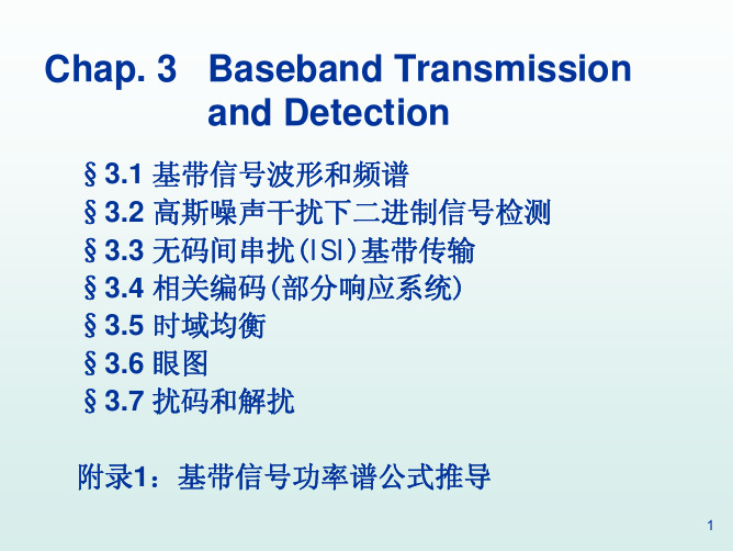
§3.1 基带信号波形和频谱 §3.2 高斯噪声干扰下二进制信号检测 §3.3 无码间串扰(ISI)基带传输 §3.4 相关编码(部分响应系统) §3.5 时域均衡 §3.6 眼图 §3.7 扰码和解扰
附录1:基带信号功率谱公式推导
¾ 采样时刻kT输出
∑ z(kT ) = bkh(0) + bnh[(k − n)T)] + no (kT) n≠k
16
式中: bk h(0)
→ 当前脉冲抽样值
∑ bnh[(k − n)T ] → 其它脉冲波形拖尾对当前脉冲
n≠k
的干扰,称为码间串扰(ISI)
no (kT ) → 抽样时刻加性噪声干扰值
=
(a1 − a2 )2 σ02
最大
问题:什么样的滤波器能对已知输入信号有最大输出 信噪比?-匹配滤波器(Matched Filter)
21
¾ 匹配滤波器(MF) :其频率传输特性与输入信号s(t) 频谱特性共轭匹配,即
H ( f ) = kS ∗ ( f )e− j 2πfT = kS (− f )e− j2πfT
10
§3.2 高斯噪声干扰下二进制信号检测 数字解调和检测
n(t)
sx(t)
发射波形
sx(t)
z(kT)
z(kT)
输出码元
最佳判决门限γo
z(kT)=ai(kT)+no(kT) 11
¾ 在二进制信道中,定义在码元(symbol)间隔(0,T)上的 发送信号可以表示为:
sx
(t
)
=
⎧⎨⎩ss21
∞
∫ h(t ) = H T ( f ) H C ( f ) H R ( f )e j 2πft df −∞ ∞ ∫= H ( f )e j 2 πft df −∞
核电子技术原理 (王芝英 着) 原子能出版社 部分课后答案

V0(s) = I0(s)·[R0∥(1/sc)]
= I0[1/(s+1/τ)]·[R0(1/sc0)/( R0+(1/sc0))
=( I0/ c0)·{1/[(s+1/τ) (s+1/ R0 c0)]}
∴
V0 (t)
= I0R0 1− R0C0 τ
⎛ −t ⎜⎜ e τ ⎝
t −
e − R0C0
⎞ ⎟⎟⎠
30 u
a: T1 共射极放大,T3,T4 两级共集电极放大 恒流源作负载,10μ自举电容,电压并联负反馈。
1
2
3
b:
T1 共基,T2 共射,T3 共集,T4,T5 互补复合跟随器。 1μ自举电容,电压并联负反馈。
3.5 极零相消电路和微分电路有什么区别?如何协调图示的参数,使 它能达到极零相消的目的?
∵
E
=
1 2
CV
2
∴V = 2E / C = 0.126V
1.9 求单个矩形脉冲 f(t)通过低通滤波器,RC=T,RC=5T,及 RC=T/5, 时的波形及频谱。
U
t
⎧0 V0 (t) = ⎪⎨1− e−(t+T / 2)/ RC
⎪⎩(1− e−T / RC )e−(t−T / 2) / RC
t <T/2 −T / 2 ≤ t ≤T / 2 t >T/2
(1)求 Vo(t)的一般表达式 (2)当 Cf=1pF, Rf=109Ω时,画出大致波形并与 Rf→∞时作比较。
(1)
⎛
⎞
⎛
∵VO ( s) = −Q ⎜⎜⎝ Rf
1 //
sC f
⎞Q ⎟⎟⎠ = − C f
⎜ ⎜
基于电流变化率的准恒频滞环电流控制方法

基于电流变化率的准恒频滞环电流控制方法顾振江;卢毅;胡应宏;刘少宇【摘要】针对滞环电流控制存在的开关频率不固定,设计输出滤波器困难的缺点,通过对开关频率与滞环环宽关系的分析,提出了一种根据电流变化率调节环宽的准恒频滞环电流控制方法.控制方法根据电流变化率来实时调节滞环控制的环宽,实现开关频率的恒定;具有响应速度快和稳定性好的优点,同时克服了滞环电流控制开关频率不固定的缺点:较已有方法计算量小,不依赖于系统参数,容易实现,并通过理论推导和仿真证实了方法的可行性和正确性.【期刊名称】《中国电力》【年(卷),期】2015(048)001【总页数】4页(P127-130)【关键词】非线性控制;可变环宽;变流器;滞环电流控制;开关频率;直接电流控制;准恒频【作者】顾振江;卢毅;胡应宏;刘少宇【作者单位】国网冀北电力有限公司管理培训中心,北京 102401;国网冀北电力有限公司电力科学研究院,北京 100045;国网冀北电力有限公司电力科学研究院,北京100045;国网新源张家口风光储示范电站有限公司,河北张家口075000【正文语种】中文【中图分类】TM761+.2;O231.2随着大容量风机以及STATCOM等电力电子设备在电力系统中应用越来越广泛,电力电子变流器的控制方法成为研究热点[1-3]。
直接电流控制被广泛应用于开关电源、变流器等电力电子控制[4-5]。
直接电流控制有线性控制和非线性控制2种方式,电流滞环控制方法因其简单可靠,容易实现,在非线性控制中广泛使用[6-7]。
固定环宽的滞环电流控制方法便于硬件实现,得到最广泛应用。
与现有的其他控制方法相比,其优点主要体现在软硬件实现难度较小、动态响应较快、对负载参数的变化不敏感、电流跟踪的误差较小等;其缺点是开关频率随着电流变化率而变化,这将增大网侧滤波电感及电容等的设计难度,增大功率模块的开关应力及开关损耗等。
可变环宽的滞环电流控制方法可以克服固定环宽的滞环电流控制存在的缺点,成为近几年研究和应用的热点[8-9]。
OFDM系统频偏估计与补偿

图 1 传统的频分复用多载波技术
图 2 OFDM 多载波调制技术
(1)串并变换 数据传输的典型形式是串行数据流,符号被连续传输,每个数据符号的频谱可占据整个
带宽。但在并行数据传输系统中,许多符号同时传输,这可以减少一些在串行系统中出现的 问题。
对于高速的数字通信系统,每个传输符号的速率能够达到每秒几万比特,如果以典型的 串行方式传输,这意味着每个符号的传输时间只有几十微秒。在如此短的时间内传输大量数 据,一旦信道产生较大的变化,尤其是在无线信道环境中,显然,误码率将会大大增加。
dt
∑ ∫ =
1 T
N −1
di
i=0
ts ts
+T
exp⎢⎣⎡
j
2π
i
− T
k
(t
−
t
s
)⎥⎦⎤
dt
=
dk
(4)
即可恢复出期望符号。对其它子载波来说,在积分间隔内频率相差整数倍个周期,故积 分结果为零。这充分体现了各子载波间的正交性。
这种正交性还可以从频域角度理解。图 3 给出了 OFDM 符号中各子载波信号的频谱图。 可以看出,在每一子载波频率的最大值处,所有其他子信道的频谱值恰好为零;也就是说, OFDM 各子载波信号之间的正交性避免了子信道间干扰(ICI)的出现。
∫1
T
T 0
exp(jωnt)
exp(jωmt)dt
=
⎧1 ⎩⎨0
m=n m≠n
(3)
例如对(2)式中的第 k 个子载波进行解调,然后在 T 内积分,即:
∫ ∑ dˆk
=1 T
ts +T exp⎜⎛−
ts
⎝
j2π
k T
数字通信(第四版)部分习题答案

Problem 4.11 : (a) As an orthonormal set of basis functions we consider the set f1 (t) = f3 (t) = 1 0≤t<1 0 o.w 1 2≤t<3 0 o.w
f2 (t) = f4 (t) =
2 2 2
|s1 − s2 |2 =
4 −2 −2 −1
2
=
25
= = =
√ √ √
5 12
14 √ 2 −3 3 3 −2 |s2 − s4 |2 = = 31 d2,4 = √ 2 0 1 3 −3 |s3 − s4 |2 = = 19 d3,4 = √ Thus, the minimum distance between any pair of vectors is dmin = 5.
⇒
(b) For non-independent information sequence the power spectrum of s(t) is given by : Φss (f ) =
1 T
|G(f )|2 Φbb (f ). But : φbb (m) = E [bn+m bn ] = E [a a ] + kE [an+m−1 an ] + kE [an+m an−1 ] + k 2 E [an+m−1 an−1 ] n+m n 2 m=0 1+k , k, m = ±1 = 0, o.w.
1 + k2 , m=0 k, m = ±4 ⇒ Φbb (f ) = 1 + k 2 + 2k cos 2πf 4T φbb (m) = 0, o.w.
MAX1448EHJ+T中文资料
D E C
10
OUTPUT DRIVERS
D9–D0
PD
REF
REFSYSTEM+ BIAS
OVDD OGND
REFOUT REFIN REFP
COM REFN
OE
Pin Configuration appears at end_______________________________________________________ Maxim Integrated Products
元器件交易网
10-Bit, 80Msps, Single 3.0V, Low-Power ADC with Internal Reference MAX1448
ABSOLUTE MAXIMUM RATINGS
VDD, OVDD to GND ...............................................-0.3V to +3.6V OGND to GND.......................................................-0.3V to +0.3V IN+, IN- to GND........................................................-0.3V to VDD REFIN, REFOUT, REFP, REFN, and COM to GND..........................-0.3V to (VDD + 0.3V) OE, PD, CLK to GND..................................-0.3V to (VDD + 0.3V) D9–D0 to GND.........................................-0.3V to (OVDD + 0.3V) Continuous Power Dissipation (TA = +70°C) 32-Pin TQFP (derate 18.7mW/°C above +70°C)......1495.3mW Operating Temperature Range ...........................-40°C to +85°C Junction Temperature ......................................................+150°C Storage Temperature Range ............................-60°C to +150°C Lead Temperature (soldering, 10s) .................................+300°C
FIB介绍
307
195
50
364
240
sample 為 Si
表面濺擊(Sputtering):
指 Ga+直接撞擊表面原子將其擊出,有下列幾項要點: Sputtering Rate: 對不同物質會有不同的濺擊速率(下表). 結晶方向不同有不同的濺擊速率.若同一平面有不同的晶粒(Grain)方向,會造成無 法平坦蝕刻(例:Cu). 無法選擇性蝕刻. 被移除的物質回積(redeposition): 無法開高視比的孔洞(high aspect hole),因為被擊出的物質撞到側壁又填回,到一 定深度後就不易再加深. 若回填物為導體,在電路修正時將會造成漏電或短路.
下圖分別顯示:Deflector 工作原理,Scanning Pattern, Rotate Image.
其他:
典型 FIB 系統 [2] : Column 長度 15 cm 2 µA(離子流)從 Source 流出 經過 spray aperture 後約 20 nA 經 limiting aperture 選擇使用 20nA - 1pA Beam Current 離子束與物質作用 離子轟擊
信号检测与估计知识点总结(2)
信号检测与估计知识点总结(2)第三章估计理论1. 估计的分类矩估计:直接对观测样本的统计特征作出估计。
参数估计:对观测样本中的信号的未知参数作出估计。
待定参数可以是未知的确定量,也可以是随机量。
点估计:对待定参量只给出单个估计值。
区间估计:给出待定参数的可能取值范围及置信度。
(置信度、置信区间) 波形估计:根据观测样本对被噪声污染的信号波形进行估计。
预测、滤波、平滑三种基本方式。
已知分布的估计分布未知或不需要分布的估计。
估计方法取决于采用的估计准则。
2. 估计器的性能评价无偏性:估计的统计均值等于真值。
渐进无偏性:随着样本量的增大估计值收敛于真值。
有效性:最小方差与实际估计方差的比值。
有效估计:最小方差无偏估计。
达到方差下限。
渐进有效估计:样本量趋近于无穷大时方差趋近于最小方差的无偏估计。
? 一致性:随着样本量的增大依概率收敛于真值。
Cramer-Rao 界:其中为Fisher 信息量。
3. 最小均方误差准则模型:假定:是观测样本,它包含了有用信号及干扰信号,其中是待估计的信号随机参数。
根据观测样本对待测参数作出估计。
最小均方误差准则:估计的误差平方在统计平均的意义上是最小的。
即使达到最小值。
此时从而得到的最小均方误差估计为:即最小均方误差准则应是观测样本Y 一定前提下的条件均值。
需借助于条)()(1αα-≥F V =????????-=2212122);,(ln );,(ln )(αααααm m y y y p E y y y p E F )(),()(t n t s t y +=θ)(t n T N ),,,(21θθθθ=),(θts {}{})?()?()?,(2θθθθθθ--=T E e E {}0)?,(?2==MSE e E d d θθθθθθθθθd Y f Y MSE )|()(??=件概率密度求解,是无偏估计。
4. 线性最小均方误差准则线性最小均方误差准则:限定参数估计结果与观测样本间满足线性关系。
光电成像原理及技术课后题答案
第一章5.光学成像系统与光电成像系统的成像过程各有什么特色?在光电成像系统性能评论方面往常从哪几方面考虑?答:a、二者都有光学元件并且其目的都是成像。
而差别是光电成像系统中多了光电装换器。
b、敏捷度的限制,夜间无照明时人的视觉能力很差;分辨力的限制,没有足够的视角和对照度就难以辨识;时间上的限制,变化过去的影像没法存留在视觉上;空间上的限制,分开的空间人眼将没法察看;光谱上的限制,人眼只对电磁波谱中很窄的可见光区感兴趣。
6.反应光电成像系统光电变换能力的参数有哪些?表达形式有哪些?答:变换系数:输入物理量与输出物理量之间的允从关系。
在直视型光电成像器件用于加强可见光图像时,被定义为电镀增益G1,光电敏捷度:或许:8.如何评论光电成像系统的光学性能?有哪些方法和描绘方式?答,利用分辨力和光学传达函数来描绘。
分辨力是以人眼作为接收器所判断的极限分辨力。
往常用光电成像系统在必定距离内能够分辨的等宽黑白条纹来表示。
光学传达函数:输出图像频谱与输入图像频谱之比的函数。
关于拥有线性实时间、空间不变性成像条件的光电成像过程,完整能够用光学传达函数来定量描绘其成像特征。
第二章6.影响光电成像系统分辨光景细节的主要要素有哪些?答:光景细节的辐射亮度(或单位面积的辐射强度);光景细节对光电成像系统接受孔径的张角;光景细节与背景之间的辐射对照度。
第三章13.依据物体的辐射发射率可见物体分为哪几种种类?答:依据辐射发射率的不一样一般将辐射体分为三类:黑体, =1;灰体, <1, 与波长没关;选择体, <1 且随波长和温度而变化。
14. 试简述黑体辐射的几个定律,并议论其物理意义。
答:普朗克公式:普朗克公式描绘了黑体辐射的光谱散布规律,是黑体理论的基础。
斯蒂芬 - 波尔滋蔓公式:表示黑体在单位面积上单位时间内辐射的总能量与黑体温度T 的四次方成正比。
维恩位移定律:他表示当黑体的温度高升时,其光谱辐射的峰值波长向短波方向挪动。
- 1、下载文档前请自行甄别文档内容的完整性,平台不提供额外的编辑、内容补充、找答案等附加服务。
- 2、"仅部分预览"的文档,不可在线预览部分如存在完整性等问题,可反馈申请退款(可完整预览的文档不适用该条件!)。
- 3、如文档侵犯您的权益,请联系客服反馈,我们会尽快为您处理(人工客服工作时间:9:00-18:30)。
TheEffectsofInterferenceThresholdandSNRHysteresisonDistributedChannelAssignmentAlgorithmsforUFDMA
D.Grace,A.G.Burr,T.C.TozerCommunicationsResearchGroup,DepartmentofElectronicsUniversityofYork,YorkYO15DDUnitedKingdom.Email:dg@ohm.york.ac.uk
Abstract:TheeffectsofinterferencethresholdandSNRacceptancethresholdonchannelcapacityhavebeende-terminedforseveraldistributedchannelassignmentalgo-rithmsusingUnsupervisedFDMA(UFDMA),amultipleac-cessschemefortheterrestrialradioenvironment.Itisfoundthattheeffectoftighteningtheinterferencethresholdre-ducesthecalldroppingprobabilityattheexpenseofincreas-ingtheblockingprobabilityforagivenchannelcapacity.In-troducinghysteresisintheSNRacceptancethresholdisonlybeneficialinimprovingperformanceifahighlevelofcalldroppingcanbetolerated,andinallcircumstancesreducescapacityforafixedcallblockinggradeofservice.Theseef-fectsarethenexplainedusingapictorialmodelwhichconsid-ersthefrequencyreusebehaviourusingtheconceptsofInter-ferenceandSNRExclusionAreas.
I.INTRODUCTION
Distributedchannelassignmentalgorithmsaregainingconsid-erableattentionasincreasingcellulartrafficrequirestheuseofsmallerandsmallercells,whichmeanthatduetolocalisedfad-ing,theportclosesttothemobilemaynolongerbethemostsuit-abletransmittertosupportthecall.Theconceptofacoexistenceetiquette,whichaimstominimisetheamountofinterferencein-flictedonotheruserswhilstallowingdifferentusers,networks,andcompaniestoshareacommonbandwidthhasbeenadoptedbytheFCCintheUSA[1].Severalalgorithmswhichmakeuseofcoexistenceetiquetteshavebeenproposed,e.g.Changhasde-velopedaPACS-UBprotocol[2]whichiscompatiblewithPACSandLaw[3]haslookedatdistributedalgorithmswithDECT.Wehaveexploredtheuseofcoexistenceetiquettesforusewithpoint-to-pointlinkswhicharetypicalinamilitaryenvironment,ratherforthancellular/cordlessarchitectures,usingaschemebasedonFDMAcalledUnsupervisedFDMA[4].UFDMAismultipleaccessschemedesignedforpoint-to-pointlinks,whichcanbeusedeitherforhighdensitycommunica-tionsystemssuchasinbuildingwirelesstelephonesystems,orhereasinthisworkforlinkswhichcouldbesignificantlylonger,m.AlthoughthispaperusesanFDMAarchitecturetoexploretheeffects,thetechniquesusedwouldbeequallyap-plicabletoaTDMAarchitecture.WeexaminetheeffectofinterferencethresholdandhysteresisintheSignaltoNoiseRatio(SNR)thresholdoncapacityusingUFDMA.Firstlyabriefoutlineofboththearchitectureandal-gorithmsaregiven.Resultsarethenexplainedusingapictorialmodel[5].II.ARCHITECTURE&ALGORITHMSUFDMAmayuseavarietyoffullyDistributedDynamicChan-nelAssignment(DDCA)algorithms,whichperformchannelse-lectionandassignmentbasedonthevalueoftwoparameters:theinterferencelevelatatransmitterpriortotransmission(thisde-termineswhetherachannelisfree);andtheSignaltoInterference+NoiseRatio(SNR)atthereceiverduringtheestablishmentofacall.Atransmittercanonlybeinitialisediftheinterferencepowerisbelowtheinterferencethreshold.Providingtheresult-inginitialSNRisaboveagiventhresholdMINSNRthenthecallisfullyestablished.IfitshouldfallbelowMINSNRduringthelifetimeofthecall,thecalliseitherdropped,ordependingonthealgorithm,reassignedtoadifferentchannel.Theserequirementsareusedtosetupeachhalfofapoint-to-pointduplexlink(theserulesformpartofthecoexistenceetiquette[2]).Otherresearchershavefoundthatthemostsuitableendtomea-suretheinterferenceleveldependsonthenetworkarchitectureandprotocols[3,6].Inthisworktheinterferencelevelismea-suredoneachchannelatthetransmitterendofthelink,usingaseparatetestreceiver.ForUFDMApoint-to-pointlinksthishasbeenfoundtobethemostsuitableendofthelinktomeasuretheinterferencelevel,bothintermsofprotocolsimplicityaswelloverallcapacityforaparticulargradeofservice[5].
Thesimulationscenarioconsidersaphysicallayermadeupofastandardtworaypropagationmodelwithpathlossincreasingasinafrequencyre-useenvironment,withallantennaheightssetat1.5m.Lognormalshadowingisincludedwithameanof0dBandstandarddeviationof8dB.Bysplittingtheeffectoftheshadowingonthecommunicationlinkequallybetweentransmitterandreceiver,thenincreasedcorrelationwithlocationcanbeprovided,i.e.interferencefrom/toaparticulartransmit-ter/receivercontainsthesamelognormalcontributionsandasaresultprovidesanintuitivelymorerealisticshadowingenviron-ment[5].Allalgorithmsassumeseparateforwardandreverselinkfrequencyallocationswith10channelsineach.Themaxi-mumnumberofchannelsthatcanbeusedineachscanallocationisdependentonchannelscanalgorithm,channelscantime,andmaximumcallsetuptimethatcanbetolerated[7].Allcallsusenegativeexponentiallydistributedcallduration(mean50s)andinterarrivaltimes.AnoisefloorofdBmisused,basedonareceivernoisetemperatureof300Kandtransmissionbandwidthof25kHz.Allalgorithmsaretestedbyconsideringthebehaviourofthesystemeachtimeacallisinitiated,ratherthanusingawork-ingprotocoltransmittingpackets,whichhasbeenadoptedpre-viously[7].Anewlyinitiatedcallcaneitherbesetupcorrectly,whichcancauseothercallssharingthesamechanneltobeeitherdroppedorreassigned,oritcanbeblocked.Monitoringtheseparticulareventsdecreasessimulationtimesconsiderably,allow-ingrealisticcalllengthstobeused,butcarehasbeentakentoen-surethatonlyinformationthatcanbegatheredatnodelevelandadoptedintheprotocolsisused.Instantaneouscallsetuptimeshavebeenusedinthesealgorithms,butsincecallsetuptimeismuchlessthanmeancalldurationandinterarrivaltime,theef-fectofthisapproximationisminimalsincecontentionisunlikelytooccurduringthesetupphase.Theeffectsofadropcalltimeoutwhichislongerthanthesetuptimeissimulated,bydrop-ping/reassigningcallswhichfailMINSNRonlyafterthenewcallhasbeensuccessfullyestablished.Fourdistributedchannelassignmentalgorithmshavebeenap-pliedtoUFDMA[8]:FirstAvailable(FA):callsareassignedonthefirstavail-ablefreechannel;LeastInterferedChannel(LIC):channelsarearrangedinorderofincreasinginterferenceandthechannelwithleastinterferenceisselectedforanewcall.Ifthisfailsthenchannelswithincreasinglevelsofinterferenceareselecteduntileitherallchannelshavebeentried,ortheinterferencethresholdisexceeded;LICwithCallReassignment:callsareassignedontheLIC,butcallsfailingduetopoorSNRarereassignedontoanewchannelaccordingtotheLICalgorithmHysteresisinSNR:callsareassignedusingtheLICalgo-rithmbutforacalltobeacceptedtheSNRatthereceivermustbegreaterthantheMINSNRthresholdbyamini-mumlevel,setbetween0-10dB.III.PERFORMANCEPARAMETERSThecallblockinganddroppingprobabilityhavebeenusedtode-terminesystemcapacity.However,measuringperformanceus-ingblockinganddropcallprobabilitycangiveamisleadingpic-tureoftheperformanceasthereisaninherenttradeoffbetweencallblockinganddropping[4].Usingtheprobabilitythatthecallisunsuccessfultakesintoaccountbothcallblockinganddrop-pingandcanbeusedasaparameterinmeasuringthecapacityofthesystemorchannel[9].Thisparameterweightsbothcallblockinganddroppingequally,answeringtheonlyreallyimpor-tantquestiontotheenduser,“Howoftenareyougoingtogetabadcall?”.Theenduseronaciviliancellularnetworkwouldliketogetthrougheverytimeheplacesacall,andforittocom-pletesuccessfully.Theprobabilitythatacallisunsuccessfulforanofferedtrafficloadisdefinedas: