A 1-Gbs, 0.7- m CMOS Optical Receiver
SDH网络保护倒换性能的测试

SDH网络保护倒换性能的测试随着电信网络越来越广泛地应用在重要业务中,如电子资金转帐、订单处理、客户服务、库存管理电子邮件和国际互联网接入等,业务生存性变得比以往更加重要。
遵循SDH标准的同步传输设备均内置了自动保护倒换(APS)算法和性能/告警监视功能,它们能保证线形点对点和同步环形拓扑网络结构在网络故障条件下具备自愈能力。
当发生设备故障或光纤断路时,线形和环形SDH网络中的自动保护倒换可以确保数据的完整性和维持服务质量(QoS)。
因此,在安装SDH网络单元(NE)时,对其自动保护倒换的操作性能进行验证是非常重要的。
然而,仅验证在检测到故障时能否启动保护倒换是不够的,为了尽量减少对传输的破坏,倒换必须在ITU-TG.783(线形网络)和ITU-TG.841(环形网络)推荐的指定时限内完成。
本文介绍了一种快速、可靠测量倒换完成时间的方法。
该方法不仅能确保网络单元符合ITU-T的推荐标准,而且还能使它们保持服务质量,从而提供一定的收益保护。
一、线形和环形网络中的保护机制线形网络通常由两个可能带有分插复用器或光学路由再生器的SDH传输终端组成,典型的例子是长途城市间路由或海底电缆系统。
为了保护单个或多路光纤传输的实际信号,线形网络机制提供了一条STM-N保护光纤,若实际工作光纤中的一条发生故障,那么终端设备自动将传输切换到保护路由上去。
对于大城市地区和全局长途路由,普遍使用环形网络。
这种环形结构的保护机制是:即使一段线路(例如AB)双向被彻底切断,但通过倒换和桥接信号仍能在A和B之间沿环路重新建立长距离路由,使双向传输重新接通。
AB方向连接称作“短路径”,长方向传输称作“长路径”。
可见,为了提供这种保护机制,在建立传输系统时必须备用50%的传输容量。
有两种办法提供这种备用容量,第一种是MS专用保护环,它的实现方法是:系统由两条环路组成,相同的业务信号在这两条相反方向旋转的环路上传输,其中一条作为业务环路,另一条作为保护环路。
雷达岗位技能考核题

一/二次监视雷达岗位技能考试题雷神二次雷达(适用于沈阳、大连两地)1.如何在RMM上显示原始视频。
(1)在实时显示状态下,单击在屏幕左侧中部“Setting”栏中的“Display Mode”按钮,进入显示选项,按下“Scan Converter”按钮,启动原始视频显示;(2)单击在屏幕左侧中部“Setting”栏中的“Video”按钮,进入视频选项,根据需要进行调整。
2.如何在RMM上切换显示单位(公制/英制)。
(1)单击在屏幕左侧中部的“Setting”栏中的“Filters”按钮,点击下一页,进入“Measurement Units”选项;(2)若选择公制,则用右上键单击“Metric”按钮,若选择英制,则用右上键单击“Imperial”按钮。
3.如何更改RMM显示地图。
(1)在实时显示状态下,单击在屏幕左侧中部“Setting”栏中的“Maps”按钮,进入地图选项;(2)在“Map Select”栏中选择想要使用的地图,当选择的地图名出现在下方的“Selectd Map”栏中时,单击旁边的“OK”按钮。
4、雷神二次雷达开机程序(1)合配电箱总开关和各分支开关;(2)将CMS和RMM电源打开;(3)打开天线控制系统上的天线开关;(4)打开询问机电源开关。
5、雷神二次雷达如何实现CHA和CHB之间的切换(1)登录CMS;(2)点击RFCO;(3)点击SWAP Channels,切换询问机工作。
6、如何在CMS进行故障隔离(1)登录CMS;(2)右键单击故障通道,选择FAULT ISOLATION 命令。
7、如何在CMS上登录透明模式(1)登录CMS;(2)选择维护模式Maintenance Mode,待询问机模块变成蓝色;(3)选择透明模式Transparent Mode。
8、如何在CMS上显示并保存全部动态参数和全部参数开关(1)登录CMS;(2)选择维护模式Maintenance Mode,待询问机模块变成蓝色;(3)选择透明模式Transparent Mode,Input 选择 Keyboard,Output 选择 File;(4)输入记录文件名;(5)输入DDP=ALL,显示全部动态参数;(6)输入DPS=ALL,显示全部参数开关。
光通信模块最全知识

MT8976资料
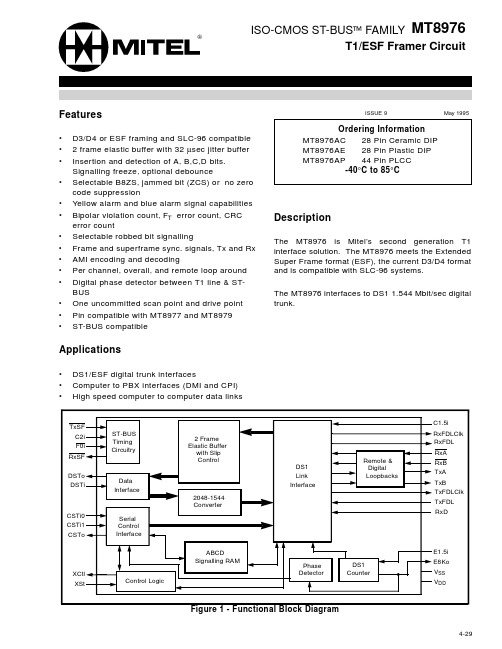
19 28
DSTi
Data ST-BUS Input. This pin accepts a 2048 kbit/s serial stream which contains the 24 PCM or data channels to be transmitted on the T1 trunk.
2048-1544 Converter
DS1 Link Interface
Remote & Digital Loopbacks
ABCD Signalling RAM
Phase
DS1
Detector
Counter
•
Figure 1 - Functional Block Diagram
C1.5i RxFDLClk RxFDL RxA RxB TxA TxB TxFDLClk TxFDL RxD
TxA
Transmit A Output. Unipolar output that can be used in conjunction with TxB and
external line driver circuitry to generate the bipolar DS1 signal.
23
error count • Selectable robbed bit signalling • Frame and superframe sync. signals, Tx and Rx • AMI encoding and decoding • Per channel, overall, and remote loop around • Digital phase detector between T1 line & ST-
DS90CR287MTD
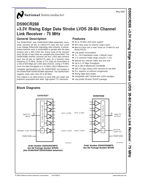
DS90CR288+3.3V Rising Edge Data Strobe LVDS 28-Bit Channel Link Receiver -75MHzGeneral DescriptionThe DS90CR287(see DS90CR287/288A datasheet)trans-mitter converts 28bits of CMOS/TTL data into four LVDS (Low Voltage Differential Signaling)data streams.A phase-locked transmit clock is transmitted in parallel with the data streams over a fifth LVDS link.Every cycle of the transmit clock 28bits of input data are sampled and transmitted.The DS90CR288receiver converts the four LVDS data streams back into 28bits of CMOS/TTL data.At a transmit clock frequency of 75MHz,28bits of TTL data are transmitted at a rate of 525Mbps per LVDS data ing a 75MHz clock,the data throughput is 2.10Gbit/s (262.5Mbytes/sec).Complete specifications for the DS90CR287are located in the DS90CR287/DS90CR288A datasheet.The DS90CR287supports clock rates from 20to 85MHz.This chipset is an ideal means to solve EMI and cable size problems associated with wide,high-speed TTL interfaces.Featuresn 20to 75MHz shift clock supportn 50%duty cycle on receiver output clockn Best-in-Class Set &Hold Times on TxINPUTs and RxOUTPUTsn Low power consumptionn Tx +Rx Powerdown mode <400µW (max)n ±1V common-mode range (around +1.2V)n Narrow bus reduces cable size and cost n Up to 2.10Gbps throughputn Up to 262.5Mbytes/sec bandwidthn 345mV (typ)swing LVDS devices for low EMI n PLL requires no external components n Rising edge data stroben Compatible with TIA/EIA-644LVDS standard n Low profile 56-lead TSSOP packageBlock DiagramsDS90CR287DS100872-1Order Number DS90CR287MTD See NS Package Number MTD56(See DS90CR287/DS90CR288A datasheet)DS90CR288DS100872-27Order Number DS90CR288MTD See NS Package Number MTD56May 2002DS90CR288+3.3V Rising Edge Data Strobe LVDS 28-Bit Channel Link Receiver -75MHz©2002National Semiconductor Corporation 查询DS90CR287MTD供应商Pin DiagramTypical ApplicationDS90CR288DS100872-22DS100872-23D S 90C R 288 2Absolute Maximum Ratings(Note1)If Military/Aerospace specified devices are required, please contact the National Semiconductor Sales Office/ Distributors for availability and specifications.Supply Voltage(V CC)−0.3V to+4V CMOS/TTL Input Voltage−0.5V to(V CC+0.3V) CMOS/TTL Output Voltage−0.3V to(V CC+0.3V) LVDS Receiver Input Voltage−0.3V to(V CC+0.3V) Junction Temperature+150˚C Storage Temperature−65˚C to+150˚C Lead Temperature(Soldering,4sec.)+260˚C Maximum Package Power Dissipation@+25˚CMTD56(TSSOP)Package:DS90CR288 1.61W Package Derating:DS90CR28812.4mW/˚C above+25˚C ESD Rating(HBM,1.5kΩ,100pF)>7kV (EIAJ,0Ω,200pF)>700V Latch Up Tolerance@+25˚C>±300mA Recommended Operating ConditionsMin Nom Max Units Supply Voltage(V CC) 3.0 3.3 3.6V Operating Free AirTemperature(T A)−10+25+70˚C Receiver Input Range0 2.4V Supply Noise Voltage(V CC)100mV PPElectrical CharacteristicsOver recommended operating supply and temperature ranges unless otherwise specifiedSymbol Parameter Conditions Min Typ Max Units CMOS/TTL DC SPECIFICATIONSV IH High Level Input Voltage 2.0V CC V V IL Low Level Input Voltage GND0.8V V OH High Level Output Voltage I OH=−0.4mA 2.7 3.3V V OL Low Level Output Voltage I OL=2mA0.060.3V V CL Input Clamp Voltage I CL=−18mA−0.79−1.5V I IN Input Current V IN=0.4V,2.5V or V CC+1.8+10µAV IN=GND−100µA I OS Output Short Circuit Current V OUT=0V−60−120mA LVDS RECEIVER DC SPECIFICATIONSV TH Differential Input High Threshold V CM=+1.2V+100mV V TL Differential Input Low Threshold−100mV I IN Input Current V IN=+2.4V,V CC=3.6V±10µAV IN=0V,V CC=3.6V±10µA RECEIVER SUPPLY CURRENTI CCRW Receiver Supply Current WorstCase C L=8pF,Worst CasePattern(Figures1,2)f=33MHz4965mAf=40MHz5370mAf=66MHz81105mAf=75MHz110130mAI CCRZ Receiver Supply Current PowerDown PWR DWN=LowReceiver Outputs Stay Low duringPowerdown Mode1055µANote1:“Absolute Maximum Ratings”are those values beyond which the safety of the device cannot be guaranteed.They are not meant to imply that the deviceshould be operated at these limits.The tables of“Electrical Characteristics”specify conditions for device operation.Note2:Typical values are given for V CC=3.3V and T A=+25˚C.Note3:Current into device pins is defined as positive.Current out of device pins is defined as negative.Voltages are referenced to ground unless otherwisespecified(except V TH and V TL).DS90CR2883Receiver Switching CharacteristicsOver recommended operating supply and temperature ranges unless otherwise specified Symbol ParameterMinTyp Max Units CLHT CMOS/TTL Low-to-High Transition Time (Figure 2)2 3.5ns CHLT CMOS/TTL High-to-Low Transition Time (Figure 2) 1.8 3.5ns RSPos0Receiver Input Strobe Position for Bit 0(Figure 8)f =75MHz0.580.95 1.32ns RSPos1Receiver Input Strobe Position for Bit 1 2.49 2.86 3.23ns RSPos2Receiver Input Strobe Position for Bit 2 4.39 4.76 5.13ns RSPos3Receiver Input Strobe Position for Bit 3 6.30 6.677.04ns RSPos4Receiver Input Strobe Position for Bit 48.208.578.94ns RSPos5Receiver Input Strobe Position for Bit 510.1110.4810.85ns RSPos6Receiver Input Strobe Position for Bit 612.0112.3812.75ns RSKM Receiver Skew Margin (when used with DS90CR287)(Note 4)(Figure 9)f =75MHz 380ps RCOP RxCLK OUT Period (Figure 3)13.33T 50ns RCOH RxCLK OUT High Time (Figure 3)f =75MHz 3.65 6.0ns RCOL RxCLK OUT Low Time (Figure 3) 3.656.0ns RSRC RxOUT Setup to RxCLK OUT (Figure 3) 3.5ns RHRC RxOUT Hold to RxCLK OUT (Figure 3)3.5ns RCCD RxCLK IN to RxCLK OUT Delay @25˚C,V CC =3.3V (Note 5)(Figure 4) 3.45.07.3ns RPLLS Receiver Phase Lock Loop Set (Figure 5)10ms RPDDReceiver Powerdown Delay (Figure 7)1µsNote 4:Receiver Skew Margin is defined as the valid data sampling region at the receiver inputs.This margin takes into account the transmitter pulse positions (min and max)and the receiver input setup and hold time (internal data sampling window-RSPOS).This margin allows LVDS interconnect skew,inter-symbol interference (both dependent on type/length of cable),and source clock (less than 250ps).Note 5:Total latency for the channel link chipset is a function of clock period and gate delays through the transmitter (TCCD)and receiver (RCCD).The total latency for the 217/287transmitter and 218/288receiver is:(T +TCCD)+(2*T +RCCD),where T =Clock period.See also DS90CR287/DS90CR288A datasheet.AC Timing DiagramsDS100872-2FIGURE 1.“Worst Case”Test PatternDS100872-5DS100872-6FIGURE 2.DS90CR288(Receiver)CMOS/TTL Output Load and Transition TimesD S 90C R 288 4AC Timing Diagrams(Continued)DS100872-10FIGURE 3.DS90CR288(Receiver)Setup/Hold and High/Low TimesDS100872-12FIGURE 4.DS90CR288(Receiver)Clock In to Clock Out DelayDS100872-14FIGURE 5.DS90CR288(Receiver)Phase Lock Loop Set TimeDS90CR2885AC Timing Diagrams(Continued)DS100872-16FIGURE 6.28Parallel TTL Data Inputs Mapped to LVDS Outputs (DS90CR287)DS100872-18FIGURE 7.Receiver Powerdown DelayD S 90C R 288 6DS90CR288 AC Timing Diagrams(Continued)DS100872-28FIGURE8.Receiver LVDS Input Strobe Position7AC Timing Diagrams(Continued)DS90CR288Pin Description—Channel Link ReceiverPin Name I/O No.DescriptionRxIN+I 4Positive LVDS differential data inputs.(Note 8)RxIN−I 4Negative LVDS differential data inputs.(Note 8)RxOUT O 28TTL level data outputs.RxCLK IN+I 1Positive LVDS differential clock input.RxCLK IN−I 1Negative LVDS differential clock input.RxCLK OUT O 1TTL level clock output.The rising edge acts as data strobe.Pin name RxCLK OUT.PWR DWN I 1TTL level input.When asserted (low input)the receiver outputs are low.V CC I 4Power supply pins for TTL outputs.GND I 5Ground pins for TTL outputs.PLL V CC I 1Power supply for PLL.PLL GND I 2Ground pin for PLL.LVDS V CC I 1Power supply pin for LVDS inputs.LVDS GNDI3Ground pins for LVDS inputs.Note 8:These receivers have input failsafe bias circuitry to guarantee a stable receiver output for floating or terminated receiver inputs.Under these conditions receiver inputs will be in a HIGH state.If a clock signal is present,outputs will all be HIGH;if the clock input is also floating/terminated outputs will remain in the last valid state.A floating/terminated clock input will result in a LOW clock output.DS100872-20C —Setup and Hold Time (Internal data sampling window)defined by Rspos (receiver input strobe position)min and max Tppos —Transmitter output pulse position (min and max)RSKM ≥Cable Skew (type,length)+Source Clock Jitter (cycle to cycle)(Note 6)+ISI (Inter-symbol interference)(Note 7)Cable Skew —typically 10ps–40ps per foot,media dependent Note 6:Cycle-to-cycle jitter is less than 250ps at 75MHz.Note 7:ISI is dependent on interconnect length;may be zeroFIGURE 9.Receiver LVDS Input Skew Margin (DS90CR287/DS90CR288A)D S 90C R 288 8Applications InformationThe DS90CR287and DS90CR288are backward compatiblewith the existing5V Channel Link transmitter/receiver pair(DS90CR283,DS90CR284).To upgrade from a5V to a3.3Vsystem the following must be addressed:1.Change5V power supply to3.3V.Provide this supply tothe V CC,LVDS V CC and PLL V CC.2.Transmitter input and control inputs except3.3V TTL/CMOS levels.They are not5V tolerant.3.The receiver powerdown feature when enabled will lockreceiver output to a logic low.However,the5V/66MHzreceiver maintain the outputs in the previous state whenpowerdown occurred.The Channel Link devices are intended to be used in a widevariety of data transmission applications.Depending uponthe application the interconnecting media may vary.Forexample,for lower data rate(clock rate)and shorter cablelengths(<2m),the media electrical performance is less critical.For higher speed/long distance applications the me-dia’s performance becomes more critical.Certain cable con-structions provide tighter skew(matched electrical lengthbetween the conductors and pairs).Twin-coax for example,has been demonstrated at distances as great as5metersand with the maximum data transfer of2.10Gbit/s.Addi-tional applications information can be found in the followingNational Interface Application Notes:AN=####TopicAN-1041Introduction to Channel LinkAN-1108PCB Design Guidelines for LVDS andLink DevicesAN-806Transmission Line TheoryAN-905Transmission Line Calculations andDifferential ImpedanceAN-916Cable InformationCABLES:A cable interface between the transmitter andreceiver needs to support the differential LVDS pairs.The21-bit CHANNEL LINK chipset(DS90CR217/218)requiresfour pairs of signal wires and the28-bit CHANNEL LINKchipset(DS90CR287/288)requires five pairs of signal wires.The ideal cable/connector interface would have a constant100Ωdifferential impedance throughout the path.It is alsorecommended that cable skew remain below130ps(@75MHz clock rate)to maintain a sufficient data sampling win-dow at the receiver.In addition to the four or five cable pairs that carry data andclock,it is recommended to provide at least one additionalconductor(or pair)which connects ground between thetransmitter and receiver.This low impedance ground pro-vides a common-mode return path for the two devices.Some of the more commonly used cable types for point-to-point applications include flat ribbon,flex,twisted pair andTwin-Coax.All are available in a variety of configurations andoptions.Flat ribbon cable,flex and twisted pair generallyperform well in short point-to-point applications while Twin-Coax is good for short and long applications.When usingribbon cable,it is recommended to place a ground linebetween each differential pair to act as a barrier to noisecoupling between adjacent pairs.For Twin-Coax cable ap-plications,it is recommended to utilize a shield on eachcable pair.All extended point-to-point applications shouldalso employ an overall shield surrounding all cable pairsregardless of the cable type.This overall shield results inimproved transmission parameters such as faster attainablespeeds,longer distances between transmitter and receiverand reduced problems associated with EMS or EMI.The high-speed transport of LVDS signals has been demon-strated on several types of cables with excellent results.However,the best overall performance has been seen whenusing Twin-Coax cable.Twin-Coax has very low cable skewand EMI due to its construction and double shielding.All ofthe design considerations discussed here and listed in thesupplemental application notes provide the subsystem com-munications designer with many useful guidelines.It is rec-ommended that the designer assess the tradeoffs of eachapplication thoroughly to arrive at a reliable and economicalcable solution.BOARD LAYOUT:To obtain the maximum benefit from thenoise and EMI reductions of LVDS,attention should be paidto the layout of differential lines.Lines of a differential pairshould always be adjacent to eliminate noise interferencefrom other signals and take full advantage of the noisecanceling of the differential signals.The board designershould also try to maintain equal length on signal traces fora given differential pair.As with any high-speed design,theimpedance discontinuities should be limited(reduce thenumbers of vias and no90degree angles on traces).Anydiscontinuities which do occur on one signal line should bemirrored in the other line of the differential pair.Care shouldbe taken to ensure that the differential trace impedancematch the differential impedance of the selected physicalmedia(this impedance should also match the value of thetermination resistor that is connected across the differentialpair at the receiver’s input).Finally,the location of theCHANNEL LINK TxOUT/RxIN pins should be as close aspossible to the board edge so as to eliminate excessive pcbruns.All of these considerations will limit reflections andcrosstalk which adversely effect high frequency performanceand EMI.TERMINATION:Use of current mode drivers requires aterminating resistor across the receiver inputs.The CHAN-NEL LINK chipset will normally require a single100Ωresistorbetween the true and complement lines on each differentialpair of the receiver input.The actual value of the terminationresistor should be selected to match the differential modecharacteristic impedance(90Ωto120Ωtypical)of the cable.Figure10shows an example.No additional pull-up or pull-down resistors are necessary as with some other differentialtechnologies such as PECL.Surface mount resistors arerecommended to avoid the additional inductance that ac-companies leaded resistors.These resistors should beplaced as close as possible to the receiver input pins toreduce stubs and effectively terminate the differential lines.DECOUPLING CAPACITORS:Bypassing capacitors areneeded to reduce the impact of switching noise which couldlimit performance.For a conservative approach threeparallel-connected decoupling capacitors(Multi-Layered Ce-ramic type in surface mount form factor)between each V CCand the ground plane(s)are recommended.The three ca-pacitor values are0.1µF,0.01µF and0.001µF.An exampleis shown in Figure11.The designer should employ widetraces for power and ground and ensure each capacitor hasits own via to the ground plane.If board space is limiting thenumber of bypass capacitors,the PLL V CC should receivethe most filtering/bypassing.Next would be the LVDS V CCpins and finally the logic V CC pins.DS90CR2889Applications Information(Continued)CLOCK JITTER:The CHANNEL LINK devices employ a PLL to generate and recover the clock transmitted across the LVDS interface.The width of each bit in the serialized LVDS data stream is one-seventh the clock period.For example,a 75MHz clock has a period of 13.33ns which results in a data bit width of 1.90ns.Differential skew (∆t within one differential pair),interconnect skew (∆t of one differential pair to another)and clock jitter will all reduce the available win-dow for sampling the LVDS serial data streams.Care must be taken to ensure that the clock input to the transmitter be a clean low noise signal.Individual bypassing of each V CC to ground will minimize the noise passed on to the PLL,thus creating a low jitter LVDS clock.These measures provide more margin for channel-to-channel skew and interconnect skew as a part of the overall jitter/skew budget.COMMON-MODE vs.DIFFERENTIAL MODE NOISE MAR-GIN:The typical signal swing for LVDS is 300mV centered at +1.2V.The CHANNEL LINK receiver supports a 100mV threshold therefore providing approximately 200mV of dif-ferential noise mon-mode protection is of moreimportance to the system’s operation due to the differential data transmission.LVDS supports an input voltage range of Ground to +2.4V.This allows for a ±1.0V shifting of the center point due to ground potential differences and common-mode noise.TRANSMITTER INPUT CLOCK:The transmitter input clock must always be present when the device is enabled (PWR DWN =HIGH).If the clock is stopped,the PWR DWN pin must be used to disable the PLL.The PWR DWN pin must be held low until after the input clock signal has been reap-plied.This will ensure a proper device reset and PLL lock to occur.POWER SEQUENCING AND POWERDOWN MODE:Out-puts of the CHANNEL LINK transmitter remain in TRI-STATE until the power supply reaches 2V.Clock and data outputs will begin to toggle 10ms after V CC has reached 3V and the Powerdown pin is above 1.5V.Either device may be placed into a powerdown mode at any time by asserting the Pow-erdown pin (active low).Total power dissipation for each device will decrease to 5µW (typical).The transmitter input clock may be applied prior to powering up and enabling the transmitter.The transmitter input clock may also be applied after power up;however,the use of the PWR DWN pin is required as described in the Transmitter Input Clock section.Do not power up and enable (PWR DWN =HIGH)the transmitter without a valid clock signal applied to the TxCLK IN pin.The CHANNEL LINK chipset is designed to protect itself from accidental loss of power to either the transmitter or receiver.If power to the transmit board is lost,the receiver clocks (input and output)stop.The data outputs (RxOUT)retain the states they were in when the clocks stopped.When the receiver board loses power,the receiver inputs are shorted to V CC through an internal diode.Current is limited (5mA per input)by the fixed current mode drivers,thus avoiding the potential for latchup when powering the device.DS100872-24FIGURE 10.LVDS Serialized Link TerminationDS100872-25FIGURE 11.CHANNEL LINK Decoupling ConfigurationD S 90C R 288 10DS90CR288 Applications Information(Continued)DS100872-26FIGURE12.Single-Ended and Differential Waveforms11Physical Dimensions inches(millimeters)unless otherwise notedLIFE SUPPORT POLICYNATIONAL’S PRODUCTS ARE NOT AUTHORIZED FOR USE AS CRITICAL COMPONENTS IN LIFE SUPPORT DEVICES OR SYSTEMS WITHOUT THE EXPRESS WRITTEN APPROVAL OF THE PRESIDENT AND GENERAL COUNSEL OF NATIONAL SEMICONDUCTOR CORPORATION.As used herein:1.Life support devices or systems are devices orsystems which,(a)are intended for surgical implantinto the body,or(b)support or sustain life,andwhose failure to perform when properly used inaccordance with instructions for use provided in thelabeling,can be reasonably expected to result in asignificant injury to the user.2.A critical component is any component of a lifesupport device or system whose failure to performcan be reasonably expected to cause the failure ofthe life support device or system,or to affect itssafety or effectiveness.National SemiconductorCorporationAmericasEmail:support@National SemiconductorEuropeFax:+49(0)180-5308586Email:europe.support@Deutsch Tel:+49(0)6995086208English Tel:+44(0)8702402171Français Tel:+33(0)141918790National SemiconductorAsia Pacific CustomerResponse GroupTel:65-2544466Fax:65-2504466Email:ap.support@National SemiconductorJapan Ltd.Tel:81-3-5639-7560Fax:81-3-5639-7507 Order Number DS90CR288MTDDimensions in millimeters onlyNS Package Number MTD56DS9CR288+3.3VRisingEdgeDataStrobeLVDS28-BitChannelLinkReceiver-75MHzNational does not assume any responsibility for use of any circuitry described,no circuit patent licenses are implied and National reserves the right at any time without notice to change said circuitry and specifications.。
GPS星历
GPS 信号结构及卫星星历。
GPS 卫星发射的信号是由载波、测距码和导航电文三部分组成的。
载波是指可运载调制信号的高频振荡波。
GPS 卫星所用的载波有两个。
由于它们均位于微波的L 波段,故分别称为L1 载波和L2 载波。
其中L1 载波是由卫星上的原子钟所产生的基准频率f0=10.23MHz 倍频154 倍后形成的,即f1=154*f0=1575.42MHz,其波长λ1 为19.03cm。
载波是基准频率f0 倍频120 L2 后形成的,即f2= 120*f0=1227.60MHz,其波长λ2 为24.42cm。
采用两个频率的目的是为了较完善地消除电离层延迟。
采用高频率载波的目的是为了更精确地测定多普勒频移,从而提高测速的精度;减少信号的电离层延迟,因为电离层延迟是与信号频率f 的平方成反比的。
测距码是用于测定从卫星到接收机之间距离的二进制码。
GPS 卫星中所用的测距码从性质上讲属于伪随机噪声码。
根据其性质和用途的不同,测距码可分为粗码(C/A 码)和精码(P 码或Y 码)两类,每个卫星所用的测距码互不相同且相互正交。
粗码C/A 码,又称为粗捕获码,它被调制在L1 载波上,是1MHz 的伪随机噪声码(PRN 码),其码长为1023 位(周期为1ms )。
由于每颗卫星的C/A 码都不一样,因此,经常用它们的PRN 号来区分它们。
C/A 码是普通用户用以测定监测站到卫星间的距离的一种主要信号。
精码P(Y)码,又称为精码,它被调制在L1 和L2 载波上,是10MHz 的伪随机噪声码,其周期为7 天。
在实施AS 时,P 码与W 码进行模二相加生成保密的Y 码,此时,一些用户无法利用P 码来进行导航定位。
导航电文是GPS 卫星向用户播发的一组反映卫星在空间的位置、卫星的工作状态、卫星钟的修正参数,电离层延迟修正参数等重要数据的二进制代码,也称数据码(D 码)。
广播星历,这种星历是主控站利用跟踪站收集的观测资料计算并外推出未来两周的星历,然后注入到GPS 卫星,形成导航电文供用户使用。
10G光模块 安捷伦公司86100D示波器介绍 2010
10Gb/s光电器件测试新挑战Hu HaiyangApplication EngineerAgilent Technologies2010-10-15Standardsand Application Testing? Agilent Technologies, Inc. 2010? Agilent Technologies, Inc. 2010内容安排?10G 光接口模块&测试标准?10G 光接口测试需求及解决方案?10G 光接口测试常见问题?86100D 简介? Agilent Technologies, Inc. 2010光收发模块的发展光接口的优点¨高带宽¨传输距离远¨电气干扰小¨可靠性高¨传输密度大经济性维护性扩展性发展方向复杂性&多样性:多标准智能化:热插拔/具有数字诊断功能高速:>10G 速率模块需求快速稳定增长高密度:并行光器件波长可调: DWDM 应用主要应用?以太网交换机?存储局域网?磁盘阵列/RAID 系统?主机总线适配器?高端服务器和网关?城域网中的路由器10G 光模块将进入稳定成长期? Agilent Technologies, Inc. 2010不同的封装光接口模块CFP LR44x10GQSFP 4x10GSNAP12 12x10G光纤通道: 1G(1x) ⇒2G(2x) ⇒4.25G(4x) ⇒8.5G(8x) ⇒14.2G(16x) ⇒40G?以太网: 1G ⇒10 G, next 25G? 40G? 100G?SFP+? Agilent Technologies, Inc. 2010MSA 多源协议MSA¡s SFP SFP+QSFP Xenpak X2XFP 300 Pin协议光纤通道以太网Sonet/SDH DWDM CWDM选件SR LR ER LRM Extended距离>100m >300m >500m >1km >10km速率(<10G)155Mb 1.0625 Gig 1.25 Gig 2.488Gig 2.5Gig 2.7Gig 3.125Gig 4.25Gig 5Gig 6.25Gig 8.5Gig速率(>10G)9.953 Gig 10.3125 Gig 10.519 Gig 10.709Gig 11.1Gig 11.3Gig? Agilent Technologies, Inc. 2010比较各种封装尺寸10Gb/s 主流产品? Agilent Technologies, Inc. 2009以太网名称如何理解描述(m ):?S: 短波长(850nm, 多模)?L: 长波长(1310nm, 主要是单模, 少量多模)?E: 扩展波长(1550nm, 单模)?T: 双绞线电缆?C: 同轴电缆(铜)?K: 背板描述(n ):?X: 8B/10B 编码?R: 64B/66B 编码?W: STS-192 封装64B/66B 编码(SONET )第2参数:?M 在-LRM 意味着多模?附加在最后的数字表明通道(lanes )数量, 比如-CX4, -LX410G BASE -(m )(n )数据速率基带传输媒质? Agilent Technologies,Inc. 200910GE网络规范?2002, IEEE802.3ae-2002包含7个光纤标准和XAUI 接口::¨10GBASE-LX4:4x3.125Gb/s, CWDM, >300m¨10GBASE-ER, -LR, -SR¨10GBASE-EW, -LW, -SW¨XAUI接口是10G以太网连接MAC 和PHY之间的电口.?2004, 10GBASE-CX4推出(IEEE802.3ak-2004):XAUI信号在同轴电缆传输(15m,4x2.5G Infiniband,预加重)?20069月.¨10GBASE-T 随IEEE802.3an-2006推出. 规范10GE在双绞线铜揽传输.¨10GBASE-LRM 随IEEE802.3aq-2006推出. 10GE在已铺设多模光纤传输?2007, IEEE802.3ap-2007:背板接口标准.¨1000BASE-KX¨1x1.25Gb/s¨10GBASE-KX4¨4x 3.125Gbps¨10GBASE-KR¨1x 10.3125Gbps10GbESwitch CardComputerBlade or LineCard 10G Electrical25G Electrical25G Optical 4 @ 25G Optical40GBASE-KR4? Agilent Technologies, Inc. 2010? Agilent Technologies, Inc. 201010G 光通信应用标准10 G 以太网( ) ¨本地网络(LAN)Overview: /w/index.php?title=10_gigabit_Ethernet&oldid=158488764?802.3ae:10 GbE: 10GBASE-SR, -LR, -ER, -SW, -LW, -EW ?802.3aq:10 Gb/s 多模光纤以太网: 10GBASE-LRM ?802.3ab:40G/100G ?SFP+ 模块被802.3aq 标准采纳光纤通道( ) ¨存储网络(SAN)Overview: /w/index.php?title=Fibre_Channel&oldid=157471662)?FC-PI-5: 物理层10x FC/16x FC ?FC-FS-5: 协议层: 帧和信令标准?其它协议层标准T11.3SFF ( ) ¨小尺寸封装Small Form Factor?SFF-8431: 8.5G & 10G 增强型SFF 即插即用模块¡SFP+¡?SFF-8432: 针对¡SFP+¡机械性能指标?SFF-8083:¡SFP+¡ 一致性板卡边沿连接器? Agilent Technologies, Inc. 2009光纤通道名称如何理解1200-SM -LC -L数据速率1 600 --1 600 MB/s 16xFC 14.02Gb/s 1 200 --1 200 MB/s 10xFC 10.3125Gb/s 800 --800 MB/s 8x FC 8.5gb/s 400 --400 MB/s 4xFC 4.25Gb/s 200 --200 MB/s 2xFC 2.125Gb/s 100 --100 MB/s 1x FC 1.063Gb/s传输媒质SM ¨单模M5 --50¦m 多模(OM2)M5E ¨50¦m 多模(OM3)M5F --50¦m 多模(OM4)M6 --62.5¦m 多模(OM1)SE ¨非平衡电接口DF ¨平衡电接口交互类型SN ¨短波长(850 nm) &限幅接收机SA --短波长(850 nm) &线性接收机LL ¨长波长(1310 nm / 1550 nm) &限幅接收机LC ¨低成本长波长(1310 nm ) &限幅接收机LZ --长波长(1490nm) &限幅接收机LA --长波长(1310 nm / 1550 nm) &线性接收机EL ¨电口&无均衡接收机EA --电口&带均衡接收机距离V ¨超长距离(>50 km)L ¨长距离(>10 km)M ¨中等距离(>4 km)I ¨短距离(>2 km)S ¨超短距离(>70 m)限幅和线性接收机V outP inV outP in? Agilent Technologies, Inc. 2010内容安排?10G 光接口模块&测试标准?10G 光接口测试需求及解决方案?10G 光接口测试常见问题?86100D 简介? Agilent Technologies, Inc. 201010G 光接口测试参数IEEE802.3ae/ab(2008)& FC-PI-5(2010)参数解释SM MM 参数解释SM MM发射机测试CW 中心波长√√接收及测试RMS BW RMS 光谱宽度√SMRR 边模抑制比√BW 20dB 谱宽√P out 平均功率√√OMA 光调制幅度√√Tr/Tf 上升/下降时间√√RIN OMA 相对噪声强度√√P over 过载功率√√ER 消光比√√JT接收抖动容限(OMA)√√TDP 色散代价√P unstress (OMA)接收灵敏度(OMA)√√TJ 总抖动√√RL 回波损耗√√DJ 确定抖动√√F 3dB 3dB 截止频率√√DDPWS 数据相关脉冲宽度收缩√√F 10dB10dB 截止频率√UJ 不相关抖动√√P Stress (OMA)压力眼图灵敏度√VECP 垂直眼图闭合代价√TWDP发射波形色散代价√? Agilent Technologies, Inc. 2010¡抖动分析¡ & ¡幅度分析¡-86100X-200抖动分析选件& 300幅度分析选件?时间噪声(抖动)/幅度噪声→眼图闭合→误码?抖动分析帮助我们探测隐藏在数据上升/下降变化边沿不在预期时间出现背后的机制. 能否采用同样的手段分析信号的幅度电平偏离理想位置??理解什么原因造成眼图闭合可以帮助我们解决问题DeterministicJitter (DJ)RandomJitter (RJ)Data DependentJitter (DDJ)Inter-symbolInterference (ISI)Duty CycleDistortion (DCD)PeriodicJitter PJTotalJitter (TJ)DeterministicInterference( (DI)RandomInterference( (RI)Data DependentInterference(DDI)Inter-symbolInterference (ISI)Periodic Interference( PI)TotalInterference(TI)周期性? Agilent Technologies, Inc. 2010光调制幅度OMAOMA: 光发射机输出信号1电平和0电平的幅度差大多数标准要求特殊的测试码型以测量OMA测试波形/不是眼图典型情况是测量如下的方波码型例如: 11111000001111100000¡.86100X-300 幅度分析选件支持任意码型(自动找到1码序列和0码序列而无论其长度新参数86100C V7.00以上版本直接支持OMA 测试N? Agilent Technologies, Inc. 2010Haiyang HU? Agilent Technologies, Inc. 20102132n+1n ? Agilent Technologies, Inc. 2010(锁定) ? Agilent Technologies, Inc. 2010A0OMAJitter为内眼的高度,垂直眼图VECP = 10* log(OMA/A0)? Agilent Technologies, Inc. 201086100X如何进行压力眼图校准测试?消光比 & 交叉点 眼图模式 码型:PRBS, ERCF ON)TJ (BER 1 e-3), RJ, DCD & ISI 抖动模式 (#200)TJ (BER 1e-2) = TJ (BER 1e-3) ¨ 2* RJ? Agilent Technologies, Inc. 20010OMA 眼图模式 码型:1100 参数: 眼图幅度)A0 (BER 1 e-3) 抖动模式/ 幅度分析 (#300), 参数: 眼张开度光域/电域色散电通道TXASIC RX光通道100 差分的 传输线多模光纤E/O O/E收发模块? Agilent Technologies, Inc. 20010Race conditions cause pulse overlap 走的路径条件不一样造成脉冲重叠预加重色散补偿 ¨ 发射机(Tx)端发射信号没有预加重接收信号N4916B 4-阶预加重转换器3.125 Gb/s发射信号 有预加重6.25 Gb/s12.5 Gb/s接收信号那些应用需要? ?>5Gb/s信号在长电缆 或 PCB中传输需要3- 和 4- 阶预加重? Agilent Technologies, Inc. 20010均衡器色散补偿 ¨ 接收机(Rx)端假设 ? 系统线形 ? 信号劣化主要由于码间干扰 (ISI) ? ISI是确定和可不补偿的经过均衡 均衡之前-86100X -201选件内置线性反馈均衡器算法s(t)TX色散通道r(t)均衡器e(t) 符号解码噪声? Agilent Technologies, Inc. 20010新的测试参数 TWDP发射机波形色散代价? 量化评估接收机眼图的相对闭合Transmitter Waveform Dispersion Penalty¨ 参考理想发射机, 理想通道,接收机噪声高斯分布¨ 代价: 信噪比由于发射机波形失真/通道色散造成的劣化? 由ClariPhy Communications, Inc.提出* for IEEE 802.3aq? 8G 光纤通道和IEEE 802.3ax (其他标准也均采纳) 都采纳这个概念系统功率预算发射机功率 最大通道损耗发射机功率 最大通道损耗TWDPSNR RN 接收机噪声SNR effective RX NoiseSNR RN* MATLAB? scripts for TWDP calculations may contain intellectual property owned by ClariPhy Communications, Inc.? Agilent Technologies, Inc. 2010TWDP 测量-86100X -201选件 外部处理? 码型锁定数据,进行捕获 ? 最高的灵活性 ? 高精度86100C DCA-J-86100X -201选件支持在线TWDP测试DCA-J +内置MATLAB? 标准数据捕获 ? 使用测量方便 ? 实时显示结果? Agilent Technologies, Inc. 20010光模块测量结果RIN 测试一致性眼图模板测试消光比/功率测试抖动分析TWDP 测试? Agilent Technologies, Inc. 2010内容安排? 10G光接口模块&测试标准 ? 10G光接口测试需求及解决方案 ? 10G光接口测试常见问题 ? 86100D简介? Agilent Technologies, Inc. 2010测量示波器带宽问题? 发射机测量结果依赖于示波器带宽¨ 带宽太大: 噪声高, 过冲, 纹波 ¨ 带宽太小: 高码间干扰, 抖动? 通用规则: 参考接收机¨ 定义测试系统的频响 ¨ 典型的4th 阶贝塞尔滤波器=汤姆逊低通滤波响应 ¨ 带宽近似于75% 数据速率? 接收机频响有一定的容限参考接收机? Agilent Technologies, Inc. 2010O/E 转换器放大器 (选件)硬件滤波采样器A/D 转换测量示波器带宽问题示波器带宽的影响不加滤波器适合:? 激光器和驱动设计 ? 光器件故障排查加滤波器适合:? 一致性验证 ? ER & OMA 调节 ? 生产质量控制? Agilent Technologies, Inc. 2010? Agilent Technologies, Inc. 2010-9.00.0 1.0 2.0摘自FC-PI-4¡A.1.2.1.1注意:8.5G 速率信号采用,进? Agilent Technologies, Inc. 2010? Agilent Technologies, Inc. 200108条或者10条等光通道? Agilent Technologies, Inc. 2010? Agilent Technologies, Inc. 20010眼图模板测试问题?标准模板¨单次冲击模板(眼图测量模式)意味着¡失败¡¨通过/失败依赖于事件速率和测量时间?统计模板¨标准: 模板失败<= BER * 采样/UI¨显著提高测试重复性, 降低不确定度?模板富余度¨用户可以在*.msk文件定义/编辑目标(100% 富余度)¨Rev 8.0 to 包括基于误码率的1-shot自动富余度测试XFP HCTBXAUI HCTB? Agilent Technologies, Inc. 2009IEEE 802.3ba 针对40G/100G 以太网Sinx/x 函数频谱? Agilent Technologies, Inc. 2010Page 37? Agilent Technologies, Inc. 2009高级眼图分析(401选件)86100X-200抖动分析软件: 最长分析数据码型<215-1 如何分析更长的数据码型的抖动呢? 86100X-401选件帮助解决这个问题。
AFBR-57R5APZ中文资料
850 nm, SFP (Small Form Pluggable), RoHS Compliant, Low Voltage (3.3 V) Digital Diagnostic Optical Transceiver Features• Fully RoHS Compliant• Diagnostic features per SFF-8472 “Diagnostic Moni-toring Interface for Optical Transceivers”• Real time monitoring of: – Transmitted optical power – Received optical power – Laser bias current – Temperature – Supply voltage• Wide temperature and supply voltage operation (-10°C to 85°C) (3.3 V ± 10%)• Transceiver specifications per SFP (SFF-8074i) Multi-Source Agree-ment and SFF-8472 (revision 9.3) – 4.25 GBd Fibre Channel operation for FC-PI 400-M5-SN-I and 400-M6-SN-I – 2.125 GBd Fibre Channel operation for FC-PI 200-M5-SN-I and 200-M6-SN-I – 1.0625 GBd Fibre Channel operation for FC-PI 100-M5-SN-I and 100-M6-SN-I • Link lengths at 4.25 GBd:– 150 m with 50 µm MMF, 70 m with 62.5 µm MMF • Link lengths at 2.125 GBd:– 300 m with 50 µm MMF, 150 m with 62.5 µm MMF • Link lengths at 1.0625 GBd:– 500 m with 50 µm MMF, 300 m with 62.5 µm MMF • LC Duplex optical connector interface conforming to ANSI TIA/EIA604-10 (FOCIS 10)• 850 nm Vertical Cavity Surface Emitting Laser (VCSEL) source technology• IEC 60825-1 Class 1/CDRH Class 1 laser eye safe • Compatible with Gigabit EthernetAFBR-57R5APZDigital Diagnostic SFP , 850 nm, 4.25/2.125/1.0625 GBd, RoHS Compliant Optical TransceiverData SheetDescriptionAvago’s AFBR-57R5APZ optical transceiver supports high-speed serial links over multimode optical fiber at signaling rates up to 4.25 Gb/s. Compliant with Small Form Pluggable (SFP) Multi Source Agreement (MSA) mechanical and electrical specifications for LC Duplex transceivers, ANSI Fibre Channel FC-PI, FC-PI-2 and com-patible with IEEE 802.3 for gigabit applications. The part is electrically interoperable with SFP conformant devices.As an enhancement to the conventional SFP interface defined in SFF-8074i, the AFBR-57R5APZ is compliant to SFF-8472 (digital diagnostic interface for optical trans-ceivers). Using the 2-wire serial interface defined in the SFF-8472 MSA, the AFBR-57R5APZ provides real time temperature, supply voltage, laser bias current, laser average output power and received input power. This information is in addition to conventional SFP base data. The digital diagnostic interface also adds the ability to disable the transmitter (TX_DISABLE), monitor for Trans-mitter Faults (TX_FAULT), and monitor for Receiver Loss of Signal (RX_LOS).Applications• Fibre channel systems – Director class switches – Fabric switches – HBA cards• Disk and tape drive arraysRelated Products• AFBR-59R5LZ: 850 nm +3.3 V LC SFF 2x7 for 4.25/2.125/1.0625 GBd Fibre ChannelInstallationThe AFBR-57R5APZ can be installed in any SFF-8074i compliant Small Form Pluggable (SFP) port regardless of host equipment operating status. The AFBR-57R5APZ is hot-pluggable, allowing the module to be installed while the host system is operating and on-line. Upon insertion, the transceiver housing makes initial contact with the host board SFP cage, mitigating potential damage due to Electro-Static Discharge (ESD).Digital Diagnostic Interface and Serial Identification The 2-wire serial interface is based on ATMEL AT24C01A series EEPROM protocol and signaling detail. Conven-tional EEPROM memory, bytes 0-255 at memory address 0xA0, is organized in compliance with SFF-8074i. New digital diagnostic information, bytes 0-255 at memory address 0xA2, is compliant to SFF-8472. The new diag-nostic information provides the opportunity for Predic-tive Failure Identification, Compliance Prediction, Fault Isolation and Component Monitoring.Predictive Failure IdentificationThe AFBR-57R5APZ predictive failure feature allows a host to identify potential link problems before system perfor-mance is impacted. Prior identification of link problems enables a host to service an application via “fail over” to a redundant link or replace a suspect device, main-taining system uptime in the process. For applications where ultra-high system uptime is required, a digital SFP provides a means to monitor two real-time laser metrics associated with observing laser degradation and pre-dicting failure: average laser bias current (Tx_Bias) and average laser optical power (Tx_Power).Compliance Prediction Compliance prediction is the ability to determine if an optical transceiver is operating within its operating and environmental requirements. AFBR-57R5APZ devices provide real-time access to transceiver internal supply voltage and temperature, allowing a host to identify potential component compliance issues. Received optical power is also available to assess compliance of a cable plant and remote transmitter. When operating out of requirements, the link cannot guarantee error free transmission.Fault IsolationThe fault isolation feature allows a host to quickly pinpoint the location of a link failure, minimizing downtime. For optical links, the ability to identify a fault at a local device, remote device or cable plant is crucial to speeding service of an installation. AFBR-57R5APZ real-time monitors of Tx_Bias, Tx_Power, Vcc, Temperature and Rx_Power can be used to assess local transceiver current operating conditions. In addition, status flags Tx_Disable and Rx Loss of Signal (LOS) are mirrored in memory and available via the two-wire serial interface. Component MonitoringComponent evaluation is a more casual use of the AFBR-57R5APZ real-time monitors of Tx_Bias, Tx_Power, Vcc, Temperature and Rx_Power. Potential uses are as debugging aids for system installation and design, and transceiver parametric evaluation for factory or field qualification. For example, temperature per module can be observed in high density applications to facilitate thermal evaluation of blades, PCI cards and systems.Figure 1. Transceiver functional diagram.Transmitter SectionThe transmitter section includes consists of the Transmit-ter Optical SubAssembly (TOSA) and laser driver circuitry. The TOSA, containing an 850 nm VCSEL (Vertical Cavity Surface Emitting Laser) light source, is located at the optical interface and mates with the LC optical connector. The TOSA is driven by a custom IC which uses the incoming differential high speed logic signal to modulate the laser diode driver current. This Tx laser driver circuit regulates the optical power at a constant level provided the incoming data pattern is dc balanced (8B/10B code, for example).Transmit Disable (Tx_Disable)The AFBR-57R5APZ accepts a TTL and CMOS compat-ible transmit disable control signal input (pin 3) which shuts down the transmitter optical output. A high signal implements this function while a low signal allows normal transceiver operation. In the event of a fault (e.g. eye safety circuit activated), cycling this control signal resets the module as depicted in Figure 4. An internal pull up resistor disables the transceiver transmitter until the host pulls the input low. Host systems should allow a 10 ms interval between successive assertions of this control signal. Tx_Disable can also be asserted via the two-wire serial interface (address A2h, byte 110, bit 6) and monitored (address A2h, byte 110, bit 7).The contents of A2h, byte 110, bit 6 are logic OR’d with hardware Tx_Disable (pin 3) to control transmitter operation.Transmit Fault (Tx_Fault)A catastrophic laser fault will activate the transmitter signal, TX_FAULT, and disable the laser. This signal is an open collector output (pull-up required on the host board). A low signal indicates normal laser operation and a high signal indicates a fault. The TX_FAULT will be latched high when a laser fault occurs and is cleared by toggling the TX_DISABLE input or power cycling the transceiver. The transmitter fault condition can also be monitored via the two-wire serial interface (address A2, byte 110, bit 2).Eye Safety CircuitThe AFBR-57R5APZ provides Class 1 (single fault tolerant) eye safety by design and has been tested for compliance with the requirements listed in Table 1. The eye safety circuit continuously monitors the optical output power level and will disable the transmitter upon detecting an unsafe condition beyond the scope of Class 1 certifica-tion. Such unsafe conditions can be due to inputs from the host board (Vcc fluctuation, unbalanced code) or a fault within the transceiver.Receiver SectionThe receiver section includes the Receiver Optical Sub-Assembly (ROSA) and the amplification/quantization circuitry. The ROSA, containing a PIN photodiode and custom transimpedance amplifier, is located at the optical interface and mates with the LC optical connector. The ROSA output is fed to a custom IC that provides post-amplification and quantization.Receiver Loss of Signal (Rx_LOS)The post-amplification IC also includes transition detection circuitry which monitors the ac level of incoming optical signals and provides a TTL/CMOS compatible status signal to the host (pin 8). An adequate optical input results in a low Rx_LOS output while a high Rx_LOS output indicates an unusable optical input. The Rx_LOS thresholds are factory set so that a high output indicates a definite optical fault has occurred. Rx_LOS can also be monitored via the two-wire serial interface (address A2h, byte 110, bit 1).Functional Data I/OThe AFBR-57R5APZ interfaces with the host circuit board through twenty I/O pins (SFP electrical connector) iden-tified by function in Table 2. The board layout for this interface is depicted in Figure 6.The AFBR-57R5APZ high speed transmit and receive interfaces require SFP MSA compliant signal lines on the host board. To simplify board requirements, biasing resistors and ac coupling capacitors are incorporated into the SFP transceiver module (per SFF-8074i) and hence are not required on the host board. The Tx_Disable, Tx_Fault, and Rx_LOS lines require TTL lines on the host board (per SFF-8074i) if used. If an application chooses not to take advantage of the functionality of these pins, care must be taken to ground Tx_Disable (for normal operation). Figure 2 depicts the recommended interface circuit to link the AFBR-57R5APZ to supporting physical layer ICs. Timing for MSA compliant control signals implemented in the transceiver are listed in Figure 4. Application SupportAn Evaluation Kit and Reference Designs are available to assist in evaluation of the AFBR-57R5APZ. Please contact your local Field Sales representative for availability and ordering details.Ordering InformationPlease contact your local field sales engineer or one of Avago Technologies franchised distributors for ordering information. For technical information, please visit Avago Technologies’ WEB page at or contact Avago Technologies Semiconductor Products Customer Response Center at 1-800-235-0312. For information related to SFF Committee documentation visit www. . CautionThere are no user serviceable parts nor maintenance requirements for the AFBR-57R5APZ. All mechanical adjustments are made at the factory prior to shipment. Tampering with, modifying, misusing or improp-erly handling the AFBR-57R5APZ will void the product warranty. It may also result in improper operation and possibly overstress the laser source. Performance degradation or device failure may result. Connection of the AFBR-57R5APZ to a light source not compliant with ANSI FC-PI or IEEE 802.3 specifications, operating above maximum operating conditions or in a manner inconsis-tent with it’s design and function may result in exposure to hazardous light radiation and may constitute an act of modifying or manufacturing a laser product. Persons performing such an act are required by law to re-certify and re-identify the laser product under the provisions of U.S. 21 CFR (Subchapter J) and TUV.Regulatory ComplianceThe AFBR-57R5APZ complies with all applicable laws and regulations as detailed in Table 1. Certification level is dependent on the overall configuration of the host equipment. The transceiver performance is offered as a figure of merit to assist the designer. Electrostatic Discharge (ESD)The AFBR-57R5APZ is compatible with ESD levels found in typical manufacturing and operating environments as described in Table 1. In the normal handling and operation of optical transceivers, ESD is of concern in two circumstances.The first case is during handling of the transceiver prior to insertion into an SFP compliant cage. To protect the device, it’s important to use normal ESD handling pre-cautions. These include use of grounded wrist straps, work-benches and floor wherever a transceiver is handled.The second case to consider is static discharges to the exterior of the host equipment chassis after installation. If the optical interface is exposed to the exterior of host equipment cabinet, the transceiver may be subject to system level ESD requirements.Table 1. Regulatory Compliance Feature Test Method Performance Electrostatic Discharge (ESD) MIL-STD-883C Class 1 (> 2000 Volts)to the Electrical Pins Method 3015.4Electrostatic Discharge (ESD) Variation of IEC 61000-4-2 Typically, no damage occurs with 25 kV when to the Duplex LC Receptacle the duplex LC connector receptacle is contacted by a Human Body Model probe. GR1089 10 contacts of 8 kV on the electrical faceplatewith device inserted into a panel. Electrostatic Discharge (ESD) Variation of IEC 801-2 Air discharge of 15 kV (min.) contact to to the Optical Connectorconnector without damage.Electromagnetic Interference FCC Class BSystem margins are dependent on customer (EMI) CENELEC EN55022 Class B board and chassis design.(CISPR 22A)VCCI Class 1Immunity Variation of IEC 61000-4-3 Typically shows no measurable effect froma 10 V/m field swept from 10 MHz to 1 ser Eye Safety and US FDA CDRH AEL Class 1 CDRH certification # 9720151-55 Equipment Type Testing US21 CFR, Subchapter J per TUV file # 72042669Paragraphs 1002.10 and 1002.12(IEC) EN60825-1: 1994 + A11 + A2 (IEC) EN60825-2: 1994 + A1(IEC) EN60950: 1992 + A1 + A2 +A3 + A4 + A11Component Recognition Underwriters Laboratories and UL File # E173874Canadian Standards Association Joint Component Recognition for Information Technology Equipment including ElectricalBusiness Equipment RoHS Compliance Less than 1000 ppm of cadmium, lead, mercury, hexavalent chromium, polybrominated biphenyls, and polybrominated biphenyl ethers.Electromagnetic Interference (EMI)Equipment incorporating gigabit transceivers is typically subject to regulation by the FCC in the United States, CENELEC EN55022 (CISPR 22) in Europe and VCCI in Japan. The AFBR-57R5APZ’s compliance to these standards is detailed in Table 1. The metal housing and shielded design of the AFBR-57R5APZ minimizes the EMI challenge facing the equipment designer.EMI Immunity (Susceptibility)Due to its shielded design, the EMI immunity of the AFBR-57R5APZ exceeds typical industry standards.FlammabilityThe AFBR-57R5APZ optical transceiver is made of metal and high strength, heat resistant, chemical resistant and UL 94V-0 flame retardant plastic.Figure 2. Typical application configuration.Figure 3. Recommended power supply filter.3.3 VNOTE: INDUCTORS MUST HAVE LESS THAN 1 Ω SERIES RESISTANCE TO LIMIT VOLTAGE DROP TO THE SFP MODULE.Notes:1. TX_FAULT is an open collector/drain output, which must be pulled up with a 4.7 k – 10 kΩ resistor on the host board. When high, this output indicates a laser fault of some kind. Low indicates normal operation. In the low state, the output will be pulled to < 0.8 V .2. TX_DISABLE is an input that is used to shut down the transmitter optical output. It is internally pulled up (within the transceiver) with a 6.8 kΩ resistor.Low (0 – 0.8 V ): Transmitter on Between (0.8 V and 2.0 V ): Undefined High (2.0 – Vcc max) or OPEN: Transmitter Disabled3. The signals Mod-Def 0, 1, 2 designate the two wire serial interface pins. They must be pulled up with a4.7 k – 10 kΩ resistor on the host board. Mod-Def 0 is grounded by the module to indicate the module is present Mod-Def 1 is serial clock line (SCL) of two wire serial interface Mod-Def 2 is serial data line (SDA) of two wire serial interface4. RX_LOS (Rx Loss of Signal) is an open collector/drain output that must be pulled up with a 4.7 k – 10 kΩ resistor on the host board. When high, this output indicates the received optical power is below the worst case receiver sensitivity (as defined by the standard in use). Low indicates normal operation. In the low state, the output will be pulled to < 0.8 V .5. RD-/+ designate the differential receiver outputs. They are AC coupled 100 Ω differential lines which should be terminated with 100 Ω differ-ential at the host SERDES input. AC coupling is done inside the transceiver and is not required on the host board. The voltage swing on these lines will be between 600 and 1600 mV differential (300 – 800 mV single ended) when properly terminated.6. VccR and VccT are the receiver and transmitter power supplies. They are defined at the SFP connector pin. The maximum supply current is 300 mA and the associated in-rush current will typically be no more than 30 mA above steady state after 2 microseconds.7. TD-/+ designate the differential transmitter inputs. They are AC coupled differential lines with 100 Ω differential termination inside the module. The AC coupling is done inside the module and is not required on the host board. The inputs will accept differential swings of 400 – 2400 mV (200 – 1200 mV single ended), though it is recommended that values between 500 and 1200 mV differential (250 – 600 mV single ended) be used for best EMI performance.Table 2. Pin DescriptionPin Name Function/Description Notes1 VeeT Transmitter Ground2 TX_FAULT Transmitter Fault Indication – High indicates a fault conditionNote 13 TX_DISABLE Transmitter Disable – Module electrical input disables on high or open Note 24 MOD-DEF2 Module Definition 2 – Two wire serial ID interface data line (SDA) Note 35 MOD-DEF1 Module Definition 1 – Two wire serial ID interface clock line (SCL) Note 36 MOD-DEF0 Module Definition 0 – Grounded in module (module present indicator) Note 37 N.C. 8 RX_LOS Loss of Signal – High indicates loss of received optical signal Note 49 VeeR Receiver Ground 10 VeeR Receiver Ground 11 VeeR Receiver Ground12 RD- Inverse Received Data Out Note 513 RD+ Received Data Out Note 514 VeeR Receiver Ground 15 VccR Receiver Power + 3.3 V Note 616 VccT Transmitter Power + 3.3 V Note 617 VeeT Transmitter Ground 18 TD+ Transmitter Data In Note 719 TD- Inverse Transmitter Data In Note 720VeeTTransmitter GroundTable 3. Absolute Maximum RatingsParameter Symbol Minimum Maximum Unit Notes Storage Temperature T S -40 100 C Note 1, 2 Case Operating Temperature T C -40 100 C Note 1, 2 Relative Humidity RH 5 95 % Note 1 Supply Voltage Vcc T, R -0.5 3.8 V Note 1, 2, 3 Low Speed Input Voltage V IN -0.5 Vcc+0.5 V Note 1Notes;1. Absolute Maximum Ratings are those values beyond which damage to the device may occur if these limits are exceeded for other than a shortperiod of time. See Reliability Data Sheet for specific reliability performance.2. Between Absolute Maximum Ratings and the Recommended Operating Conditions functional performance is not intended, device reliabilityis not implied, and damage to the device may occur over an extended period of time.3. The module supply voltages, V CC T and V CC R must not differ by more than 0.5 V or damage to the device may occur.Table 4. Recommended Operating Conditions Parameter Symbol Minimum Maximum Unit Notes Case Operating Temperature T C -10 85 °C Note 1, 2 Supply Voltage Vcc T, R 2.97 3.63 V Note 2 Data Rate 1.0625 4.25 Gb/s Note 2 Notes:1. The Ambient Operating Temperature limitations are based on the Case Operating Temperature limitations and are subject to the host systemthermal design.2. Recommended Operating Conditions are those values for which functional performance and device reliability is implied.Table 5. Transceiver Electrical Characteristics (T C = -10°C to 85°C, VccT, VccR = 3.3 V ±10%) Parameter Symbol Minimum Typical Maximum Unit Notes AC Electrical CharacteristicsPower Supply Noise Rejection (peak-peak) PSNR 100 mV Note 1 DC Electrical CharacteristicsModule Supply Current I CC 210 mA Power Dissipation P DISS 765 mWLow Speed Outputs: V OH 2.0 VccT,R+0.3 V Note 2 Transmit Fault (TX_FAULT), Loss of Signal V OL 0.8 V(RX_LOS), MOD-DEF 2Low Speed Inputs: V IH 2.0 Vcc V Note 3 Transmit Disable (TX_DIS), V IL 0 0.8 VMOD-DEF 1, MOD-DEF2Notes:1. Filter per SFP specification is required on host board to remove 10 Hz to 2 MHz content.2. Pulled up externally with a 4.7 k – 10 kΩ resistor on the host board to3.3 V.3. Mod-Def1 and Mod-Def2 must be pulled up externally with a4.7 k – 10 kΩ resistor on the host board to 3.3 V.Table 6. Transmitter and Receiver Electrical Characteristics (T C = -10°C to 85°C, VccT, VccR = 3.3 V ±10%) Parameter Symbol Minimum Typical Maximum Unit Notes High Speed Data Input: V I 400 2400 mV Note 1 Transmitter Differential Input Voltage (TD +/-)High Speed Data Output: Vo 600 1600 mV Note 2 Receiver Differential Output Voltage (RD +/-)Receiver Contributed Total Jitter TJ 0.26 UI Note 3 (4.25 Gb/s) 62 psReceiver Contributed Total Jitter TJ 0.26 UI Note 3 (2.125 Gb/s) 124 psReceiver Contributed Total Jitter TJ 0.22 UI Note 3 (1.0625 Gb/s) 205 psReceiver Electrical Output Rise & Fall Times tr, tf 50 150 ps Note 4 (20-80%)Notes:1. Internally AC coupled and terminated (100 Ohm differential).2. Internally AC coupled but requires an external load termination (100 Ohm differential).3. Contributed DJ is measured on an oscilloscope in average mode with 50% threshold and K28.5 pattern. Contributed TJ is the sum of contrib-uted RJ and contributed DJ. Contributed RJ is calculated for 1x10-12 BER by multiplying the RMS jitter (measured on a single rise or fall edge) from the oscilloscope by 14. Per FC-PI (Table 13 - MM jitter output, note 1), the actual contributed RJ is allowed to increase above its limit if the actual contributed DJ decreases below its limits, as long as the component output DJ and TJ remain within their specified FC-PI maximum lim-its with the worst case specified component jitter input.4. 20%-80% electrical rise & fall times measured with a 500 MHz signal utilizing a 1010 data pattern.Table 7. Transmitter Optical Characteristics(T C = -10°C to 85°C, VccT, VccR = 3.3V ±10%) Parameter Symbol Minimum Typical Maximum Unit Notes Modulated Optical Output Power (OMA) Tx,OMA 247 µW Note 1(Peak-to-Peak) 4.25 Gb/sModulated Optical Output Power (OMA) Tx,OMA 196 µW Note 2(Peak-to-Peak) 2.125 Gb/sModulated Optical Output Power (OMA) Tx,OMA 156 µW Note 3(Peak-to-Peak) 1.0625 Gb/sAverage Optical Output Power Pout -9.0 dBm Note 4, 5 Center Wavelength l C 830 860 nm Spectral Width – rms s,rms 0.85 nmOptical Rise/Fall Time (4.25 Gb/s) tr, tf 90 ps 20% - 80% RIN 12 (OMA) RIN -118 dB/Hz Transmitter Contributed Total Jitter (4.25 Gb/s) TJ 0.25 UI Note 660 ps Transmitter Contributed Total Jitter (2.125 Gb/s) TJ 0.25 UI Note 6120 ps Transmitter Contributed Total Jitter (1.0625 Gb/s) TJ 0.27 UI Note 6252 psPout TX_DISABLE Asserted P OFF -35 dBmNotes:1. An OMA of 247 µW is approximately equal to an average power of –8 dBm, avg assuming an Extinction Ratio of 9 dB.2. An OMA of 196 µW is approximately equal to an average power of –9 dBm, avg assuming an Extinction Ratio of 9 dB.3. An OMA of 156 µW is approximately equal to an average power of –10 dBm, avg assuming an Extinction Ratio of 9 dB.4. Max Pout is the lesser of Class 1 safety limits (CDRH and EN 60825) or receiver power, max.5. Into 50/125 µm (0.2 NA) multi-mode optical fiber.6. Contributed DJ is measured on an oscilloscope in average mode with 50% threshold and K28.5 pattern. Contributed TJ is the sum of contributedRJ and contributed DJ. Contributed RJ is calculated for 1x10-12 BER by multiplying the RMS jitter (measured on a single rise or fall edge) from the oscilloscope by 14. Per FC-PI (Table 13 - MM jitter output, note 1), the actual contributed RJ is allowed to increase above its limit if the actual contributed DJ decreases below its limits, as long as the component output DJ and TJ remain within their specified FC-PI maximum limits with the worst case specified component jitter input.Table 8. Receiver Optical Characteristics(T C = -10°C to 85°C, VccT, VccR = 3.3 V ±10%)Parameter Symbol Min. Typ. Max. Unit Notes Input Optical Power [Overdrive] P IN 0 dBm, avgInput Optical Modulation Amplitude OMA 61 µW, OMA Notes 1, 2(Peak-to-Peak) 4.25 Gb/s [Sensitivity]Input Optical Modulation Amplitude OMA 49 µW, OMA Notes 1, 3(Peak-to-Peak) 2.125 Gb/s [Sensitivity]Input Optical Modulation Amplitude OMA 31 µW, OMA Notes 1, 4(Peak-to-Peak) 1.0625 Gb/s [Sensitivity]Stressed Receiver Sensitivity 138 µW, OMA 50/125 µm fiber, Note 5(OMA) 4.25 Gb/s 148 µW, OMA 62.5/125 µm fiber, Note 5 Stressed Receiver Sensitivity 96 µW, OMA 50/125 µm fiber, Note 6(OMA) 2.125 Gb/s 109 µW, OMA 62.5/125 µm fiber, Note 6 Stressed Receiver Sensitivity 55 µW, OMA 50/125 µm fiber, Note 7(OMA) 1.0625 Gb/s 67 µW, OMA 62.5/125 µm fiber, Note 7 Return Loss 12 dBLoss of Signal – Assert P A 27.5 µW, OMA-30 -17.5 dBm, avg Note 8Loss of Signal - De-Assert P D 31 µW, OMA-17.0 dBm, avg Note 8Loss of Signal Hysteresis P D - P A 0.5 dBNotes:1. Input Optical Modulation Amplitude (commonly known as sensitivity) requires a valid 8B/10B encoded input.2. An OMA of 61 µW is approximately equal to an average power of –14 dBm, avg with an Extinction Ratio of 9 dB.3. An OMA of 49 µW is approximately equal to an average power of –15 dBm, avg with an Extinction Ratio of 9 dB.4. An OMA of 31 µW is approximately equal to an average power of –17 dBm, avg with an Extinction Ratio of 9 dB.5. 4.25 Gb/s stressed receiver vertical eye closure penalty (ISI) min. is 1.67 dB for 50 µm fiber and 2.14 dB for 62.5 µm fiber. Stressed receiver DCD component min. (at TX) is 20 ps.6. 2.125 Gb/s stressed receiver vertical eye closure penalty (ISI) min. is 1.26 dB for 50 µm fiber and 2.03 dB for 62.5 µm fiber. Stressed receiver DCD component min. (at TX) is 40 ps.7. 1.0625 Gb/s stressed receiver vertical eye closure penalty (ISI) min. is 0.96 dB for 50 µm fiber and 2.18 dB for 62.5 µm fiber. Stressed receiver DCD component min. (at TX) is 80 ps.8. These average power values are specified with an Extinction Ratio of 9 dB. The loss of signal circuitry responds to valid 8B/10B encoded peak to peak input optical power, not average power.Table 9. Transceiver SOFT DIAGNOSTIC Timing Characteristics(T C = -10°C to 85°C, VccT, VccR = 3.3 V ±10%)Parameter Symbol Minimum Maximum Unit Notes Hardware TX_DISABLE Assert Time t_off 10 µs Note 1 Hardware TX_DISABLE Negate Time t_on 1 ms Note 2 Time to initialize, including reset of TX_FAULT t_init 300 ms Note 3 Hardware TX_FAULT Assert Time t_fault 100 µs Note 4 Hardware TX_DISABLE to Reset t_reset 10 µs Note 5 Hardware RX_LOS DeAssert Time t_loss_on 100 µs Note 6 Hardware RX_LOS Assert Time t_loss_off 100 µs Note 7 Software TX_DISABLE Assert Time t_off_soft 100 ms Note 8 Software TX_DISABLE Negate Time t_on_soft 100 ms Note 9 Software Tx_FAULT Assert Time t_fault_soft 100 ms Note 10 Software Rx_LOS Assert Time t_loss_on_soft 100 ms Note 11 Software Rx_LOS De-Assert Time t_loss_off_soft 100 ms Note 12 Analog parameter data ready t_data 1000 ms Note 13 Serial bus hardware ready t_serial 300 ms Note 14 Write Cycle Time t_write 10 ms Note 15 Serial ID Clock Rate f_serial_clock 400 kHzNotes:1. Time from rising edge of TX_DISABLE to when the optical output falls below 10% of nominal.2. Time from falling edge of TX_DISABLE to when the modulated optical output rises above 90% of nominal.3. Time from power on or falling edge of Tx_Disable to when the modulated optical output rises above 90% of nominal.4. From power on or negation of TX_FAULT using TX_DISABLE.5. Time TX_DISABLE must be held high to reset the laser fault shutdown circuitry.6. Time from loss of optical signal to Rx_LOS Assertion.7. Time from valid optical signal to Rx_LOS De-Assertion.8. Time from two-wire interface assertion of TX_DISABLE (A2h, byte 110, bit 6) to when the optical output falls below 10% of nominal. Measuredfrom falling clock edge after stop bit of write transaction.9. Time from two-wire interface de-assertion of TX_DISABLE (A2h, byte 110, bit 6) to when the modulated optical output rises above 90% ofnominal.10. Time from fault to two-wire interface TX_FAULT (A2h, byte 110, bit 2) asserted.11. Time for two-wire interface assertion of Rx_LOS (A2h, byte 110, bit 1) from loss of optical signal.12. Time for two-wire interface de-assertion of Rx_LOS (A2h, byte 110, bit 1) from presence of valid optical signal.13. From power on to data ready bit asserted (A2h, byte 110, bit 0). Data ready indicates analog monitoring circuitry is functional.14. Time from power on until module is ready for data transmission over the serial bus (reads or writes over A0h and A2h).15. Time from stop bit to completion of a 1-8 byte write command.。
KAT-330 AIS Transceiver 产品说明书
World’s most sophisticated AIS TransceiverKAT-330Class A / Inland AIS TransceiverFeaturesMeets IMO Resolutions: A.694 (17), MSC.191 (79),MSC.74 (69), ITU-R M.1371-5 (2014)Meets FCC, USCG, IC, TC, CCNR (Inland AIS)Chart display available by C-MAP MAX (on a Non-SOLAS or Inland vessel only)Simple menu display with iconsWater and weather proof (IPX6 & IPX7)Power rectifierJunction BoxSolid lines: Standard devices and connections Dashed lines: Optional devices and connections Dashed-dotted line: Owner supply10.8 to 31.2VDC100 / 115 VAC 200 / 230 VACKAT-330VHF antennaNMEA 2000Marine radarGPS compassECDIS Marine radarGPS navigator(IMO)GPS navigator (non IMO)DGPS GYRO HeadingGNSS Antenna• Design and specifications are subject to change without notice.ModelKAT-3301 W or 12.5 W (automatic selection)5 inch, color LCD with adjustable backlight Output powerDisplay size and type 800 × 480 pixelsDisplay resolution 156.025 MHz to 162.025 MHz TX / RX frequency 50 Ω156.525MH Channel 70)Impedance DSC receiver25 kHzChannel bandwidth EPFS Typically 26 seconds Position fixing system*Time to first fix (Cold start)* 2.5 m CEP / 5.0 m SEP without differential correctionAccuracy* 2.0 m CEP / 3.0 m SEP with SBAS or RTCM DGPS correctionGerman, Greek, English, Spanish, French, Italian, Japanese,Korean, Dutch, Portuguese, Russian, ChineseLanguages IEC61162-1 / -2ABM, ACA, ACK, AIR, BBM, DTM, GBS, GGA, GLL, GNS, HDT, LRF, LRI, RMC, ROT, SSD, VBW, VSD, VTG, EPV, SPW, THSInput data formats and sentences IEC61162-1 / -2ABK, ACA, ALR, LR1, LR2, LR3, LRF, LRI, TXT, VDM, VDO,TRL, VEROutput data formats and sentences Sensor data input portsIEC61162-1 / -2 3 ports 4800 baud or 38400 baud Bi-directional data portsIEC61162-1 / -2 3 ports 4800 baud or 38400 baudNMEA ports Target list, Voyage data setting, Target plot, Chart*,Messages, Alarms, Own dynamic data, System settings (*The chart feature is only enabled when this Class A AIS transceiver is operating on a non-SOLAS or inland vessel.)Presentation modesTX Malfunction, RX Channel x malfunction,Antenna VSWR exceeds limit, External EPFS lost,No valid COG, No valid SOG, Heading lost or invalid, No valid ROT, No sensor position in use, UTC Sync Invalid, Nav Status Incorrect, Active AIS SART, Internal / External GNSS mismatch, Heading sensor offsetAlarms 32 channels GPS and GLONASS operating modesReceiver channels*L1 GPS band, 1575.42 MHz and L1 GLONASS band 1597.1 to 1609.5 MHz < -107 dBm for 20% PER (TDMA Transmitter / Receiver) -107 dBm@BER < 10-2 (DSC Receiver)Frequency*10.8 to 31.2 VDC Power supply 12 W or less Power Consumption (24 VDC)Sensitivity*Operating temperature-15°C to +55°C Display unitGNSS antenna For details, please contact:Bracket moulding, Bolts, Nut, Washer, Spring washer Display unit (AIS Transceiver)Standard Equipment-40℃ to +80℃Water protection * Internal GNSSIPX6, IPX7Display unitGNSS antennaIP67EnvironmentalOptionKAT-330.MU Connecting cable and one end plain (2 m)DC cable and one end plain (2 m)Connecting cable and one end plain (2 m)With antenna cable and TNC connectors on the both sides (10 m)Mounting bracket Product mounting template, Fixings, Operation manual, Product CD,Quick installation guide, Quick operation guide, Mounting accessoriesPower rectifier, AC power cable, Junction boxPower cable14 way data accessory cable 18 way data accessory cable GNSS Antenna18-11, Printed in Japan。
移动通信原理与系统(北京邮电出版社)课后习题答案
②
③ ,所以多普勒扩展为
2.6若 , ,移动台沿电波传播方向行驶,求接收信号得平均衰落率。
解:
2.7已知移动台速度 , ,求对于信号包络均方值电平 得电平通过率。
解: ,
2.8设基站天线高度为 ,发射频率为 ,移动台天线高度为 ,通信距离为 ,利用Okumura-Hata模型分别求出城市、郊区与乡村得路径损耗。(忽略地形校正因子得影响)
微观分集:用于合并两个或多个短时限瑞利信号,这些信号都就是同一接收基站长经独立得衰落路径接收来自两个或多个不同天线发射得信号。
移动通信中常用得微观分集:时间分集、频率分集、空间分集、角度分集、极化分集。
4.3工作频段为 模拟移动电话系统TACS得信令采用数字信号方式。其前向控制信道得信息字A与B交替采用重复发送5次,如图所示。每字(40bit)长度5ms。为使字A(或B)获得独立得衰落,移动台得速度最低就是多少?
所谓相位连续就是指不仅在一个元码持续时间连续而且在从元码 转换得时刻 两个元码相位也相等满足关系式 即要求当前元码得初相位 由前一元码得初相位 来决定。
3.8GMSK系统空中接口传输速率为270、83333kbit/s,求发送信号得两个频率差。若载波频率就是 ,这两个频率又等于多少?
解:(1) ,
(2) ;
2.1说明多径衰落对数字移动通信系统得主要影响。
答:①信息信号分散,信噪比低,传输语音与数据质量不佳;
②可能引入尖锐得噪声,照成传输数据大量出错;
③不同路径传来得信号互相相关,难以直接叠加。增加接收电路单元得复杂度,从而提高系统得建设与运营成本。
2.2若某发射机发射功率为100W,请将其换算成d Bm与dBW。如果发射机得天线增益为单位增益,载波频率为900MHz,求出在自由空间中距离天线100m处得接收功率为多少dBm?
- 1、下载文档前请自行甄别文档内容的完整性,平台不提供额外的编辑、内容补充、找答案等附加服务。
- 2、"仅部分预览"的文档,不可在线预览部分如存在完整性等问题,可反馈申请退款(可完整预览的文档不适用该条件!)。
- 3、如文档侵犯您的权益,请联系客服反馈,我们会尽快为您处理(人工客服工作时间:9:00-18:30)。
IEEEJOURNALOFSOLID-STATECIRCUITS,VOL.34,NO.7,JULY1999971A1-Gb/s,0.7-972IEEEJOURNALOFSOLID-STATECIRCUITS,VOL.34,NO.7,JULY1999
(a)(b)Fig.2.Simple(a)single-stageand(b)three-stagevoltageamplifier.
highforstability.Equation(1)canthenbesimplifiedto
.Equivalently,themaximalbandwidthforagiventransimpedancegainisalsoachievedwithamaximizedvoltagegain.
ofthesucceedingstage(
canbedefinedas[2]INGELSANDSTEYAERT:1-Gb/s,0.7-isequallyreduced.Thetransistorislessinitslinearregion,and
reducesanddynamiccompressionisachieved[5].WiththeN-wellconnectedtothesource,thiseffectismuchlesspronounced,andthefeedbackresistanceispracticallyconstantfortheinputcurrentrangeofinterest.Themajordisadvantageofthisapproachistheloadingofthetransimpedanceamplifier’soutputnodewiththewellcapacitance.Furthermore,thesignalontheoutputiscapacitivelycoupledtothebulkviatheN-well-to-bulkjunctionsothatnoisecouldbeinjectedintothesubstrate.
C.IntegratedInput-ReferredNoisewithLimitedFeedbackResistor
ThenoiseperformanceofatransimpedanceamplifierisanalyzedthroughthebasiccircuitofFig.4.Theresistor’s
noiseismodeledbyitscurrentnoisesourcenoiseisnotconsidered,asitisonlyimportantatfrequenciesbelowourinterest.For
and
[6].Thisconclusionisneverthelessbasedontheassumptionthat
higherthanthereceiver’sbandwidth.Theintegratedinput-referredcurrentnoisepoweristhengivenby974IEEEJOURNALOFSOLID-STATECIRCUITS,VOL.34,NO.7,JULY1999(18)Thisfactorisintroducedin(17).Itsoptimalvalue,whichcor-respondswiththeminimalnoise,isobtainedbydifferentiatingthatequationto
andcorrespondswithanoiseintegrationuptohighfrequencieswheretheamplifier’snoisecontributionisdominant.Thisfactorisconfinedbythevoltageamplifier’sbandwidth.Inasingle-stageamplifier,itsmaximalvalueisgivenby
mtechnology.Smallvariationsfromtheoptimalvaluewillnotaffectthenoisetoomuch.Theknowledgethatissmallerthan
mCMOStechnology,themaximalvoltagegainfora500-MHzclosed-loopbandwidth,requiredfora1-Gb/snonreturn-to-zero-codeddatarate,isachievedwithasinglestage.Theamplifier’ssecondpoleisplacedatapproximately1.5GHz.Anoptimizedvoltagegainlargerthantwoisachieved,whichcorrespondstoagain-bandwidthproductofover3GHz.Thereceiverisdesignedforatotalphotodiodecapacitanceof800fFatitsinput.Thisincludesboththediodeandthe
Fig.5.OptimalCgs=CdiodeforvariousFandft0.7-mCMOS,=1;XA=2:5;Vgs0Vt=200mV.
Fig.6.A1-Gb/stransimpedancepreamplifier.bondpadcapacitance.Itissufficientfortheuseofanexternalcommercialdiode.ThetransimpedanceamplifierisloadedbyapostamplifierintegratedonthesamechipanddescribedinSectionIV.Thecarefuldesignandlayoutofthisstagelimitsitscapacitiveloadingto80fF.Accordingto(3),a1-kINGELSANDSTEYAERT:1-Gb/s,0.7-(22)with
3-dBfrequency.Thebiascircuitwouldindeedcompensatethis,resultinginadegradedbiasing.Asmultipleinvertersarecascadedineachloop,theirbandwidthsmustbesufficientlylargerthanthesignal’sbandwidth.Theyaredesignedwitha1.5-GHzbandwidth.Standardinvertersdonotachievesuchahighsmall-signalbandwidthduetotheirlargegain.Bylimitingit,thebandwidthisboosted.Themodifiedhigh-speedinverterispresentedinFig.10(a).AnNMOSdiode-coupledtransistor(
ofthediode(976IEEEJOURNALOFSOLID-STATECIRCUITS,VOL.34,NO.7,JULY1999(a)(b)Fig.10.(a)High-speedinverterand(b)high-speedlevelshifter.
Fig.11.OTAcomparatorwithlow-passfilter.enhancesits
resistorisreplacedbyaPMOStransistorinitslinearregion.Toobtainaverylowpole,the10-pFcapacitor
Afromthesingle5-Vpowersupply.TheoutputvoltageoftheOTAbiasesthelevelshifterthroughasecondlow-passfilterthatcompensatesthezerointroducedbytheMillercapacitance.Thissecondfilterconsistsofa220-k)anda5-pFcapacitor.NotethatthisisacapacitortothepowersupplytokeeptheINGELSANDSTEYAERT:1-Gb/s,0.7-
signalsource’soutputandthereceiver’sinput.Thephotodiode’scapacitanceismodeledbya500-fFcapacitor.Itaddsuptothereceiver’sinputbondpadcapacitancetoatotalof800fF.Thetran-simpedanceamplifierconsumesapproximately5mAfromasingle5-Vpowersupply.Itachievesa1-k
Hzfrom1to500MHz.Thecompleteopticalreceiver,includingtransimpedanceamplifierandpostamplifierswiththeirbiasingcircuitsandreplicas,consumesapproximately20mAfromthesingle5-Vpowersupply.Theoutputofthecircuitiscoupleddirectlytothe50-
upto5V.Themeasuredoutputsignalisthereforescaleddowntoapproximately1V.Fig.14showsameasuredeyediagramat1-Gb/sthroughput.Asensitivityofbetterthan10
mCMOS.Thecircuitfeaturesa1-kAwasachieved.ThecircuitdemonstratestheimportanceofCMOSinfuturecommunicationlinks.Fullintegration,highgain,highsensitivity,andaspeedinthegigabitareaarecompatiblewithCMOStechnologies.
REFERENCES
[1]K.Makie-Fukuda,T.Kikuchi,T.Matsuura,andM.Hotta,“Mea-surementofdigitalnoiseinmixed-signalintegratedcircuits,”IEEEJ.Solid-StateCircuits,vol.30,pp.87–92Feb.1995.[2]M.SteyaertandW.Sansen,“Opampdesigntowardmaximumgain-bandwidth,”inAnalogCircuitDesign.Norwell,MA:KluwerAca-demic,1993,pp.63–85.[3]K.R.LakerandW.M.C.Sansen,DesignofAnalogIntegratedCircuitsandSystems.NewYork:McGraw-Hill,1994.[4]D.M.Pietruszynski,J.M.Steiniger,andE.J.Swanson,“A50-Mbit/sCMOSmonolithicopticalreceiver,”IEEEJ.Solid-StateCircuits,vol.23,pp.1426–1433,Dec.1998.[5]M.Ingels,G.VanderPlas,J.Crols,andM.Steyaert,“ACMOS18THzOhm240Mb/stransimpedanceamplifierand155Mb/sLED-driverforlowcostopticalfiberlinks,”IEEEJ.Solid-StateCircuits,vol.29,pp.1552–1559,Dec.1994.[6]M.K.BarnoskiandS.D.Personick,FundamentalsofOpticalFiberCommunications.London,U.K.:Academic,1981.[7]M.Nakamura,N.Ishihara,Y.Akazawa,andH.Kimura,“Aninstan-taneousresponseCMOSopticalreceiverICwithwidedynamicrangeandextremelyhighsensitivityusingfeed-forwardauto-biasadjustment,”IEEEJ.Solid-StateCircuits,vol.30,pp.991–997,Sept.1995.