Sb_2S_3纳米线合成和表征
外文翻译(英文)纳米结构-Bi2S3的制备及其特性

Preparation of Nanostructures and Photoluminescence B i2S 3ZHANG Weixin,QIU Mo,ZHANG Junjun,YANG Zeheng,CHEN Min(School of Chemical Engineering, Hefei University of Technology, Anhui Key Laboratory of Controllable Chemical Reaction & Material Chemical Engineering, Hefei 230009, China )Abstract: Bismuth nitrate and sodium sulfide as raw material, two-step hydrothermal method was successfully prepared at 100℃Bi2S3 orthorhombic micro ring; Youyi bismuth nitrate and thiourea as the raw material, the use of step hydrothermal synthesized at 150℃with Orthorhombic's Bi2S3 nanorods. Respectively, X-ray diffraction, field emission scanning electron microscopy, transmission electron microscopy and fluorescence spectrometry and other means of final product testing phase, morphology and properties were characterized to explore the mechanism of ring formation Bi2S3 microns. The results showed that: Bi2S3 micron diameter ring 1 ~ 1.5μm, external diameter of 1.5 ~ 2μm, the average size of about 100nm in the nano-grains assembled. Bi2S3 nanorods diameter of about 125nm, a length of 1 ~ 2μm. Bi2S3 micron and nano-rod Bi2S3 ring emission peak at 447nm and 470nm are located at, Bi2S3micron emission peak position of ring Bi2S3 nanorods compared to the emission peak position was a blue shift.Key words:bismuth sulfide; hydrothermal method; nanostructure; photoluminescenceThe performance of nano-materials depends not only on its own structure and composition, but also the size and shape and materials are closely related, and thus the size of nano-materials, structure and morphology of control synthesis to optimize material properties, not only has important Theoretical significance but also broaden the application areas of nano-materials, which has become the field of synthetic chemistry and materials research focus of a front, causing researchers [1] wide interest. Because of its central ring has a very special hole and has many special properties. For example: Aizpurua other study found that the hole in the center gold ring has a strong effect of uniform magnetic field, which makes research in sensing and spectroscopy can be used as nano-hole resonance to support or test other smaller nano-structured materials . [2] In addition, Rothman magnetic ring and other materials found in high density magnetic storage and magnetic random access memory also has potential practical applications. [2]The vulcanized bismuth(Bi2S3) is a kind of important semiconductor material, its band gap is a 1.2~1.7 evs, give or get an electric shock in the thermal, optoelectronics and electrochemistry[3 –5] keep aspects like hydrogen,etc to have potential application worth.In recent years, Na rice the composition of the structure vulcanized bismuth caused the extensive concern of the researcher. Currently, at Na rice structure the vulcanized bismuth contain a lot of wires that report, mainly have a Na rice[the 6], Na rice is good[7], Na rice necklace[8] and pan-like in shape[5] and rose-like in shape[9] etc. construction structure.The Li waits[5] with the chlorinationbismuth is in the hydrochloric acid aqueous solution water solution income chlorination oxidizing bismuth for forerunner body, with sulfur generation An for sulfur source, in 60℃often press down to make from the diameter about the 30 nms, length for the Na rice of the 150~200 nms rod weave of average diameter for the thin pan-like in shape vulcanized bismuth of 2 μm. The thou national prosperity waits[9] with just the right amount of laurel acis the sulfur An salt(salt of 2-undecy 1-1-dithioureido-ethyl- imidazoline, SUDEI) for surface live agent, take chlorination bismuth and sulfur generation Mao An as raw material, adopt melting agent thermal legal system have the rose-like in shape spheroid(diameter about one μm) structure that is applied by the slab-like in shape vulcanized bismuth curl overlay.Also have the jot the search concerning vulcanized bismuth nanotube to report moreover.For example, is firm and uncompromising to wait[10] take the nitric acid bismuth and the vulcanized sodium as to respond raw material, adopt water thermal law to respond a 12h under 120℃and made a vulcanized bismuth nanotube.The experiment takes the nitric acid bismuth and the vulcanized sodium as raw material, under the sistuation that didn't make use of any mold plate, adopt two water thermal composition law, successfully made vulcanized bismuth micron ring.Inquired into the forming mechanism of the vulcanized bismuth micron ring.Rice for carrying on a compare with the vulcanized bismuth micron ring gaining in the structure, performance, and then adopting hot legal system of one-step water to have vulcanized bismuth Na pared the luminescence quality of these two kinds of different faciallook vulcanized bismuths.1. Test1.1 The preparation of sampleThe raw material that experiment uses for the vulcanized sodium, have no water ether, nitric acid bismuth, sulfur Mao, 16 alkyl three A radicle bromines to turn An and sulfuric acid.Above the trying an agent all tries an agent for the analysis purely domestic chemistry, the experiment is used water as distilled water.Two water thermal law makes the step of Bi2S3 micron ring as follows: Square one water is hot:Call to take a 0.05 gs 16 alkyls three A radicle bromines turn An(cetyl trimethyl ammonium bromide, CTAB) to put into a 150 mL the beaker and join 40 mL distilled water, then put beaker on the magnetic force stirrer constantly the rabbling make CTAB resolve full.Call again to take the 0.2 g nitric acid bismuth to put to go into beaker, go on to mix blend certain time.Then hang a muddy liquid of income to transfer an inner lining the 50 mL high pressure pot gathering four fluorine ethylenes amid, place again to take out after the constant temperature 7h in 100℃ovens, natural cooling, use distilled water to wash away dirt sediments for many times, then get forerunner thing.The second treads water thermal:Will up gain a forerunner thing to put to go into prosperous have a 40 mL of in the beaker of distilled water, then put the beaker to constantly mix blend on the magnetic force stirrer, again use to move a liquid tube to move to take a little amount solution concentration to go into beaker for the 0.6 mol/L vulcanized sodium dropand go on to mix blend certain time.Hang a muddy liquid of income to transfer an inner lining the 50 mL high pressure pot gathering four fluorine ethylenes amid, place again to take out after the constant temperature 4h in 100℃ovens, natural cooling, use distilled water to wash away dirt sediments for many times.Sparse sulfuric acid dissolution:Will up gain sediments to put to go into prosperous have a 20 mL of concentration for the beaker of 2 mol/L sparse sulfuric acid solution, the indoor temperature stat after placing about the 8 hs uses distilled water, have no water ether wash away dirt sediments for many times and dry in 60℃it, then get Bi2S3 micron ring.The one-step water thermal law makes the step of the rod of the Bi2 S3 Na rice as follows:Call to take the 0.1 g nitric acid bismuth and 0.2 g sulfur Mao to put into a 150 mL the beaker and join 40 mL distilled water, then put beaker on the magnetic force stirrer constantly rabbling, receive black to hang a muddy liquid.Hang a muddy liquid of this black to take out after transfering to the apposition in the 50 mL high pressure pot in the constant temperature 14h in 150℃ovens, natural e distilled water and have no water ether to wash away dirt sediments for many times, the sample dries in 60℃, then get the Bi2S3 Na rice rod.1.2 Outcome tokenUse D/max –xrd type the X shoot wire Yan to shoot(X-ray diffraction, XRD) instrument to carry on thing phase analysis to the sample.Take Cu K αas to radiate a source, λ =0.15418 nms, take care of the voltage as 40 kvs, take care of the current as 100 nms, scan range in 10 °~70 °.Use theaccelerating voltage as JEOL of the 10 kvs 7500 B type the field firing Hitachi of scanning the electric mirror(field-emission scan-ning electron microscopy, FESEM) and the accelerating voltage 200 kvs –800 deeply shoot electron micorscope(Transmission elec-tron microscopy, TEM)the facial look and structure of the token e Hitachi F–4500 fluorescence spectrophotometers(fluorospectro-ph- otometry, PL), the excitation light source testings the fluorescence spectrum of sample under the indoor temperature for the Xe lamp.2. Result and discussion2.1 XRD of outcome is analyticalFigure 1 is two water thermal law and one-step water thermal law income outcome of XRD table.Figure 1 amid of table wire 1 and table wire 2 difference be thermal for two water law and one-step water thermal law income outcome of XRD table.All can the beacon change into the quadrature phase Bi2S3.(JCPDF, No.06–0333)The reaction temperature of two water thermal law responds for 100℃, one-step water thermal law carrying on under 150℃ .From figure 1 amid can discover:One-step water thermal law's gaining the Yan of outcome to shoot peak intensity is higher than two water thermal the law gain outcome.Respond a temperature exaltation, the Yan of sample shoots peak enhancement, the quasi peak breadth narrows down, this instruction with respond temperature scale - up, outcome crystal exaltation for turning a degree.Fig.1 X-ray diffraction (XRD) patterns of the products prepared via the two-step hydrothermal method and the one-step hydrothermal method2.2 The Bi2 S3 micron annular becomes mechanism analysisForming mechanism of by way of to Bi2S3 micron ring progress quest, made use of FESEM and TEM to observe square one water thermal system of the facial look and structure of the forerunner thing.Figure 2 is the FESEM and TEM photograph of Bi2S3 micron ring forerunner thing.From the figure 2 as it is thus clear that:Forerunner thing from a great deal of biscuit-like in shape circle slab composition, it unipole the diameter of the biscuit-like in shape circle slab is about 1~2 μ ms, thickness is 300~500 nms.Passing Gao Bei's FESEM photograph can observe a forerunner thing further of circular biscuit-like in shape structure.(see figure 2-b) The illustration of left bottom corner is a forerunner thing side - view in the figure 2-b of high double FESEM photograph, can discover circular biscuit from a lot of Na rice circle slab rule earth the overlay apply together but forming of several structure, Na rice circle the slab is very thin, thickness for 25~50 nm.The TEM photograph of Bi2 S3 micron ring forerunner thing further recognizes that the forerunner thing presents a solid form, the diameter is about 2 μ m.(see figure 2 cs)Contrast figure 2 can discover:End outcome Bi2S3 and forerunner thing the fundamental kept consistent on the diameter and the thickness.Fig.2 FESEM and TEM photographs of the precursors of Bi2S3Figure 3 for predict according to the above-mentioned result of the possible forming process of the vulcanized bismuth micron ring diagrammatic drawing.First, Bi(NO3)3enter water solution to receive a biscuit-like in shape forerunner thing in 100℃water thermal condition.Then, the sulfur ion ahead gets rid of an outside layer of thing surface and bismuthion the reaction forming Bi2S3housings.Along with the progress for responding, the thickness of Bi2 S3 housingses enlarges gradually, inside the forerunner thing of the layer pit continuously diminish.Because the sulfur ion in the solution is that the quantity isn't enough, responds progress after a period of time the thickness of the Bi2 S3 housingses will because of sulfur ionic scarcity but stop enlarging, have to arrive hard forerunner like this the thing check –Bi2 S3 housing form structure.End, check the forerunner thing that hasn't responded complete to resolve with the sparse sulfuric acid aqueous solution of 2 mol/L, forminged Bi2 S3 micron ring.Fig.3 Schematic illustration for the formation of Bi2S3Microring2.3 The luminescence of the Na rice structure Bi2 S3The size, facial look and crystalline degree etc. of Na rice material will effect the luminescence quality of material to some extent.[11–12] Bi2S3 micron rings and Na rice are good to measure while stiring up the wavelength as 325 nms of fluorescence spectrum.Can discover:2 kinds of outcomes all have more apparent fluorescence luminescence peak, the Bi2S3 micron ring luminescence peak is located in a 447 nm, the luminescence peak of the Na rice rod form Bi2S3 is located in a 470 nm, the Bi2S3 micron ring luminescence peak is compared to a Na rice rod the luminescence peak of the form Bi2S3 obviously took place blue to move.This may be in order to constituting the Na rice of Bi2S3 micron ring opposite Bi2S3 Na rice rod Cu of grain and having more apparent size effect and resulting in.3. Conclusion(1) With Bi(NO3)3H2O5 and Na2SH2O are raw materials, adopt two water thermal law, make from the average size about is the Na rice bore of grain construction but become with 100 nms for the 1~1.5 μm and external diameter for the quadrature of 1.5~2 μm crystal train Bi2S3 micron ring;Again with the Bi(NO3)35 H2O and sulfur Mao for raw material, adopt one-step water thermal law, make a diameter about the 125 nm, length for the quadrature of 1~2 μm crystal train Bi2S3 Na rice rod.(2)The facial look of outcome as to it's the fluorescence quality contain important impact.The luminescence peak of Bi2S3micron ring and Na rice rod-like in shape Bi2S3 is located in 447 nm and 470 nm respectively, Bi2 S3 micron ring's giving out light the location of peak is compared to a Na rice rod the location of luminescence peak of the form Bi2S3 obviously took place the blue move, may be because constitute the Bi2S3 micron ring of Na rice grain opposite Bi2S3 Na rice rod the Cu has more apparent size effect. Reference:[1] PENG X. Nanomechanical oscillations in a single-C60 transistor [J]. Nature, 2000, 407: 57–60.[2]HU.α-Fe2O3 nanorings prepared by a microwave-assisted hydrothermal process and their sensing properties [J]. Adv Mater, 2007, 19(17): 2324–2330.[3]KAMAT. Photoelectrochemical behavior of Bi2S3 nanoclusters and nanostructured thin films [J]. Langmuir, 1998, 14(12): 3236–3241.[4] LIUFU. Assembly of one-dimensional nanorods into Bi2S3 films with enhanced thermoelectric transport properties [J]. Appl Phys Lett, 2007, 90(11): 112106.[5] LI. Topotactic transformation of single-crystalline precursor discs into disc-like Bi2S3 nanorod networks [J]. Adv Funct Mater, 2008, 18(8): 1194–1201.[6]LI. Synthesis and electrical transport properties of single-crystal antimony sulfide nanowires [J]. J Phys Chem C, 2007, 111: 17131–17135.[7]Shu Guang Chen Hong wei Liao The preparation and token of vulcanized bismuth(Bi2 S3) Na rice rod[J]. Nonferrous metal in Hunan, 2007, 23:(6) 33 –35.[8]LUDOVICO. Large-scale synthesis of ultrathin Bi2S3 necklace nanowires [J]. Angewandte Chem, Int Ed, 2008, 47(20): 3814–3821.[9]GU Guohua,.WANG Wei, Lü Weili, et al. Rare Met Mater Eng (in Chinese), 2007, 36: 108–111.[10]ZHU Gangqiang, LIU Peng, ZHOU Jianping, et al. Chem J Chin Univ (in Chinese). 2008, 29(2): 240–243.[11] TIAN Hongye, HE Rong, GU Hongchen. J Funct Mater (in Chinese), 2005, 36(10): 1564–1567.[12] ZENG Huidan, QIU Jianrong, GAN Fuxi, et al. J Chin Ceram Soc (in Chinese), 2003, 31(10): 974–980.。
碳化硅纳米线的制备及其吸波性能的表征

d o i :10.3963/j .i s s n .1674-6066.2024.02.002碳化硅纳米线的制备及其吸波性能的表征雷 煜1,徐 慢1,2,朱 丽1,2,石和彬1,2,沈永李1,李 想1(1.武汉工程大学材料科学与工程学院,武汉430205;2.武汉工程大学湖北省环境材料与膜工程技术研究中心,武汉430074)摘 要: 以淀粉和硅溶胶为原料,利用化学气相沉积法制备了碳化硅纳米线,并对纳米线的成分㊁形貌㊁结构及介电与吸波性能进行了分析与探讨㊂所制得的纳米线纯度较高㊁长度较长,形成了网状结构,且纳米线具有较好的吸波性能,在很大范围内均表现突出㊂关键词: 碳化硅; 纳米线; 化学气相沉积; 吸波性能P r e p a r a t i o na n dC h a r a c t e r i z a t i o no fW a v eA b s o r b i n g P r o pe r t i e s of S i CN a n o w i r e s L E IY u 1,X U M a n 1,2,Z HUL i 1,2,S H IH e -b i n 1,2,S H E NY o ng -l i 1,L IX i a n g 1(1.S ch o o l o fM a t e ri a l sS c i e n c e a n dE n g i n e e r i n g ,W u h a n I n s t i t u t e o fT e c h n o l o g y ,W u h a n430205,C h i n a ;2.E n g i n e e r i n g R e s e a r c hC e n t e r o fE n v i r o n m e n t a lM a t e r i a l s a n d M e m b r a n eT e c h n o l o g y o fH u b e i P r o v i n c e ,W u h a n I n s t i t u t e o fT e c h n o l o g y ,W u h a n430074,C h i n a )A b s t r a c t : S i l i c o n c a r b i d en a n o w i r e sw e r e s y n t h e s i z e db y c h e m i c a l v a p o rd e p o s i t i o nu s i n g st a r c ha n ds i l i c as o l .T h e c o m p o s i t i o n ,m o r p h o l o g y ,s t r u c t u r e ,d i e l e c t r i c a n dw a v e a b s o r b i n g p r o p e r t i e s o f n a n o w i r e sw e r e a n a l yz e d a n d d i s c u s s e d .T h eS i Cn a n o w i r e sh a v eh i g h p u r i t y ,l o n g l e n g t ha n d f o r m e d a n e t w o r k s t r u c t u r e ,a n d t h ew a v e a b s o r b i n gp r o p e r t i e s o f S i Cn a n o w i r e s a r e o u t s t a n d i n g i naw i d e r a n g e .K e y wo r d s : s i l i c o n c a r b i d e ; n a n o w i r e ; c h e m i c a l v a p o r d e p o s i t i o n ; w a v e a b s o r b i n gp r o p e r t y 收稿日期:2023-11-20.作者简介:雷 煜(1999-),硕士生.E -m a i l :1078750027@q q.c o m 自纳米材料被发现以来,一维纳米材料由于其特殊的结构发展迅速,其中碳化硅纳米线(S i C n w )以其独特的兼具纳米材料和陶瓷材料的性能而受到广泛关注㊂作为一种一维纳米材料,其具有宽带隙㊁高热导率㊁高介电损耗等性质,这使得它们在半导体㊁光电子㊁吸波㊁电磁屏蔽和催化等先进功能材料领域中具有巨大的应用潜力[1,2]㊂另一方面,S i C 纳米线还具有部分陶瓷材料的性能,如低密度㊁高热传导率㊁低热膨胀系数㊁化学性能稳定㊁耐热腐蚀等优异的物理㊁化学性能,在高温或极端使用条件下,具有优异的强度㊁韧性㊁摩擦㊁抗蠕变㊁隔热等综合性能,广泛应用于航空航天㊁石油化工㊁太空反射镜㊁雷达等环境中[3,4]㊂吸波材料是一种能够将电磁波吸收或反射,达到大幅度减少被保护器件接收到电磁波的效果,从而减少电磁波干扰的材料㊂碳化硅是目前非常重要的第三代宽禁带半导体材料,β-S i C 的电阻率大于103Ω㊃c m ,不仅有吸波潜能,还能减弱红外信号,是国内外发展较快的吸波材料之一[5]㊂由于其在高温下有化学稳定性,在高温吸波领域,S i C 纳米线受到了更多重视㊂传统工艺制备的碳化硅材料,其电阻率过高㊁介电虚部较低,导致吸波性能较差,不能直接作为吸波材料,需进一步对其进行掺杂改性或者复合其他材料使用㊂而S i C 纳米线由于其特殊的一维纳米材料性能,使吸波性能得到了较大的改善,是近年来研究的重点[6]㊂1 原材料与测试方法1.1 碳化硅纳米线的制备取5g 玉米淀粉㊁13.3g 硅溶胶和35g 水于烧杯中,90ħ下水浴加热,直到溶液凝固成凝胶,待凝胶冷建材世界 2024年 第45卷 第2期却后放入冷冻干燥机中,冻干48h 后取出并用玛瑙研钵研磨成粉末状㊂取10g 粉末于坩埚中,盖上坩埚盖,放入管式炉,通入氩气作为保护气体,在1300ħ下保温6h ,降温后取出㊂放入马弗炉中于600ħ下煅烧3h ,冷却至室温后取出㊂将取出后的样品放入塑料杯中,置于1m o l /L 氢氟酸溶液中酸洗,静置24h 后,用去离子水多次反复冲洗至中性,放入烘箱中干燥备用㊂1.2 制作同轴环取一定量所得纳米线于研钵中进行分散,称取0.2g 左右备用㊂按质量比为1ʒ5的比例称取相应的碳化硅纳米线粉和石蜡㊂先将1.0g 左右石蜡加入烧杯中置于90ħ水浴锅中加热㊂石蜡受热融化后再加入相应质量的碳化硅纳米线粉,不断搅拌使其混合均匀,然后停止加热㊂混合物冷却凝固后,将粘结在烧杯内壁上的混合固体刮下,重新加热熔融使粉末和石蜡混合更为充分㊂最后,将处于黏流态的混合物在专用的模具中压制成内径3mm ㊁外径7mm ㊁厚度在2~4mm 的同轴环样品㊂1.3 产物测试与表征使用X 射线衍射仪(D 8-D i s c o v e r 型,德国B r u c k e r (布鲁克)公司)对S i C 纳米线进行物相分析,扫描范围为10ʎ~80ʎ,扫描速度为2ʎ/m i n ,步长为0.02ʎ;使用场发射扫描电子显微镜(F E S E M ,J S W -5510L V 型,日本电子株式会社)观察S i C 纳米线的表面形貌,加速电压为20k V ;使用网络矢量分析仪(3671D 型,中电思仪科技股份有限公司)测试同轴环样品吸波性能,测试频率在2~18G H z ,工作模式为双端口扫频模式㊂2 结果与讨论2.1物相分析通过X 射线衍射仪对所制备的S i C 纳米线进行物相和结构表征,根据获得数据绘制X R D 图谱,如图1所示㊂从图1中可以看出,S i C纳米线的特征峰十分尖锐,说明所合成的S i C 纳米线结晶良好㊂另外,图中的五个特征峰与3C -β-S i C (P D F 卡片29-1129)吻合,属于F 43m 空间群,指标化结果获得晶格常数a =0.4359n m ,其特征峰依次对应(111)㊁(200)㊁(220)㊁(311)㊁(222)五个晶面,2θ值为33.74ʎ处并未出现大多数文献所出现的由于原子层错排形成的堆垛层错引起的超结构衍射峰,说明所合成的S i C 纳米线纯度较高,无其他晶相㊂2.2 F E S E M 分析图2为S i C 纳米线的F E S E M 照片,在显微镜下进行观察,可以发现纳米线的长度较长,为几百微米,部分达到了1mm ,而其直径约为100n m 左右㊂所合成的纳米线拥有非常高的纯度和均一性,纳米线之间相互缠绕交织成网状结构,其中残留的颗粒状物质较少,说明纳米线的纯度较高㊂2.3 S i C 纳米线的介电性能图3展示了所制S i C 纳米线介电实部和介电虚部数值随频率的变动趋势和变动范围㊂由图3可知,所制碳化硅纳米线介电常数的实部在6~7之间,虚部在0~3.5之间㊂介电实部与文献中提到的碳化硅纳米线粉体介电实部在7附近较为吻合,介电虚部波动较大,只在6~16H z 范围内与文献中提到的碳化硅纳米线粉体介电虚部在0~1对应上了,其他频率内介电虚部均偏大,从而可使得在这些频率内吸波层的储电能力和损耗能力增强㊂其原因可能是制备所得的碳化硅纳米线相互缠绕,形成了网状结构,使得整体结构内表面积增加,从而拥有较好的吸波性能㊂建材世界 2024年 第45卷 第2期根据测试所得的复介电常数和复磁导率计算出了电磁波纳米线同轴环的吸波性能框图和吸波性曲线见图4~图6㊂从图4上可以明显地看到三条尖锐的深峰,其顶点分别代表三处具有比其附近反射损耗值都高的地方,反射损耗在此取得极大值㊂从图5可以看出,在频率为9.2G H z㊁厚度为4.0mm处有最大反射损耗值,为44.70d B㊂另外频率为9.84G H z㊁厚度为3.8mm和频率为8.8G H z㊁厚度为4.2mm处也有较大反射损耗值,分别为30.71d B㊁28.62d B㊂同时在它们的附近有吸波性能良好的等高线,反射损耗值达23.14d B㊂由图6可以更清晰地看到吸波性能在不同厚度的变化,随着厚度的递增,最大反射损耗向着低频率的方向移动㊂当厚度为8mm时,出现两个反射损耗值极值,分别是4.32G H z和16.16G H z㊂材料的有效微波吸收处是其反射损耗小于-10d B处㊂当所在频率为9.2G H z㊁厚度为4mm 时,最低反射损耗-44.70d B,微波吸收频段出现在6.88~11.04G H z,其总的吸收带宽为4.16G H z㊂所合成的碳化硅纳米线吸收带宽较宽,可能是因为纳米线的长宽比较大,提升了吸波性能㊂3结论以玉米淀粉为碳源,硅溶胶为硅源合成了碳化硅纳米线㊂采用X R D对其检测分析,图谱中衍射峰强而尖锐,且与X R D卡片吻合,说明所制备的碳化硅为较纯的β-S i C且结晶很好㊂采用F E S E M对其观察,发现所制备的碳化硅纳米线长度较长,为几百微米,且纳米线互相缠绕,形成了网状结构㊂制备的纳米线具有较好的吸波性能,在很大范围内均表现突出㊂在频率为6~10G H z㊁厚度4~8mm内均有吸波能力,微波吸收的带宽为4.16G H z㊂最大反射损耗值为44.7d B,出现在厚4.0mm㊁频率9.2G H z处㊂随着厚度的不断增大,最大反射损耗值将出现在更小频率下㊂(下转第21页)3结语研究了不同掺量下的废铜渣对水泥胶凝材料的性能影响㊂研究发现,随着废铜渣掺量的增加,水泥胶凝材料的强度先增加后降低,最佳掺量为水泥用量的10%,此条件下水泥砂浆3d抗折㊁抗压强度分别为4.7M P a和27.4M P a,28d抗折㊁抗压强度分别为8.6M P a和48.7M P a㊂该研究有望能大范围处理废铜渣并用于建材领域㊂参考文献[1]雷庆关,张城,潘崇根,等.水泥基复合胶凝材料改性聚合物修补砂浆的试验研究[J].安徽建筑大学学报,2023,31(3):8-15.[2]朱茂兰,肖妮,谭良春,等.铜渣还原活化制备新型胶凝材料与矿山充填的应用[J].中国有色金属学报,2020,30(11):2736-2745.[3]母维宏,和森,周新涛,等.铜渣/电解锰渣基磷酸盐胶凝材料的制备及其形成机理探讨[J].化学工程,2020,48(10):23-28,51.[4]贾行伟,宋向荣,罗中秋,等.铜渣基磷酸盐胶凝材料的制备及其性能研究[J].硅酸盐通报,2018,37(5):1503-1508.[5]杜海云,马倩敏,郭荣鑫,等.铜渣-水泥复合胶凝材料力学性能研究[J].硅酸盐通报,2017,36(5):1634-1638,1645.[6]王茹,王高勇,张韬,等.稻壳灰在丁苯聚合物/水泥复合胶凝材料凝结硬化过程中的作用[J].硅酸盐学报,2017,45(2):190-195.[7]薛兴勇,韩要丛,苏俏俏,等.铜渣基磷酸盐胶凝材料的力学性能与微观结构[J].硅酸盐通报,2023,42(5):1750-1757.[8]张冉玥,杨仕教,杨晴,等.铜渣磁选预处理对铜渣基胶凝材料活性和抗压强度的影响[J].中国有色冶金,2023,52(1):98-106.(上接第9页)参考文献[1]刘洋涛.碳化硅纳米线的制备及吸波性能研究[D].呼和浩特:内蒙古工业大学,2022.[2]李雪婷.碳化硅纳米线基多元吸波材料的制备与性能研究[D].西安:西安建筑科技大学,2021.[3] N a k a t aSY,U e s u g iA,S u g a n oKJ,e t a l.S t r a i nE n g i n e e r i n g o fC o r e-s h e l l S i l i c o nC a r b i d eN a n o w i r e s f o rM e c h a n i c a l a n dP i e z o r e s i s t i v eC h a r a c t e r i z a t i o n s[J].N a n o t e c h n o l o g y,2019,30(26):1361-1374.[4] C h e n J J,S h iQ,X i nLP,e t a l.AS i m p l eC a t a l y s t-f r e eR o u t e f o rL a r g e-s c a l eS y n t h e s i so fS i C N a n o w i r e s[J].J o u r n a l o fA l l o y s a n dC o m p o u n d s,2011,509(24):6844-6847.[5]牛芳旭.碳化硅及其复合材料的制备与电磁波吸收性能研究[D].济南:山东大学,2019.[6] K u a n g JL,J i a n g P,H o uXJ,e t a l.D i e l e c t r i cP e r m i t t i v i t y a n d M i c r o w a v eA b s o r p t i o nP r o p e r t i e so fS i C N a n o w i r e sw i t hD i f f e r e n tL e n g t h s[J].S o l i dS t a t eS c i e n c e s,2019,91:73-76.。
硫化锑纳米材料的合成及其应用
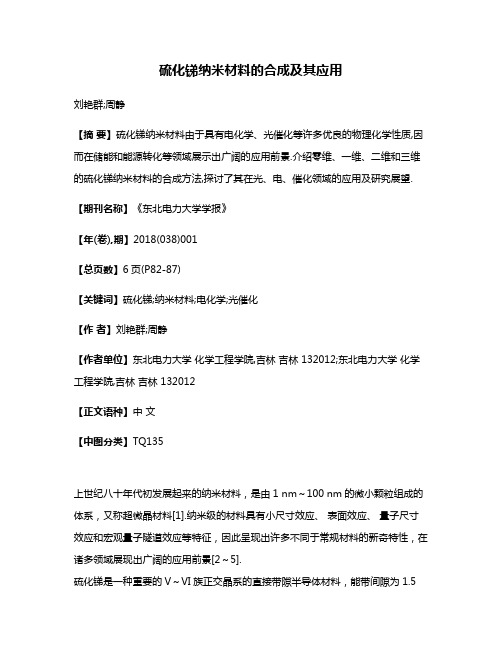
硫化锑纳米材料的合成及其应用刘艳群;周静【摘要】硫化锑纳米材料由于具有电化学、光催化等许多优良的物理化学性质,因而在储能和能源转化等领域展示出广阔的应用前景.介绍零维、一维、二维和三维的硫化锑纳米材料的合成方法,探讨了其在光、电、催化领域的应用及研究展望.【期刊名称】《东北电力大学学报》【年(卷),期】2018(038)001【总页数】6页(P82-87)【关键词】硫化锑;纳米材料;电化学;光催化【作者】刘艳群;周静【作者单位】东北电力大学化学工程学院,吉林吉林 132012;东北电力大学化学工程学院,吉林吉林 132012【正文语种】中文【中图分类】TQ135上世纪八十年代初发展起来的纳米材料,是由1 nm~100 nm的微小颗粒组成的体系,又称超微晶材料[1].纳米级的材料具有小尺寸效应、表面效应、量子尺寸效应和宏观量子隧道效应等特征,因此呈现出许多不同于常规材料的新奇特性,在诸多领域展现出广阔的应用前景[2~5].硫化锑是一种重要的V~VI族正交晶系的直接带隙半导体材料,能带间隙为1.5eV~2.2 eV[6~8],具有良好的光导性、光敏性和极高的热电性能[9].目前研究者们采用了不同方法制备出不同形貌的Sb2S3纳米材料,并探索其在不同领域的性能应用[10~12].本文论述了不同维度Sb2S3纳米材料的合成及其相关应用研究.1 不同形貌Sb2S3纳米材料根据纳米尺度的维数,可以将纳米材料划分为:零维(原子团簇和超微粒子等)、一维(纳米管、线等)、二维(纳米薄膜、多层膜等)以及三维材料(原子团簇及超微粒子的组成体等).目前国内外研究报道了零维、一维、二维以及三维纳米Sb2S3纳米材料的合成方法,典型形貌如图1所示.图1 不同维度Sb2S3纳米材料SEM图 (a)零维球状[13](b)一维管状[15](c)一维线状[16](d)二维带状[22](e)三维橄榄状[27](f)三维树枝状[28]1.1 零维Sb2S3纳米材料纳米颗粒是零维纳米材料的典型代表,一般为球形或类球形,其粒径分布窄、分散性良好.Senthil等[13]以C2H4N2S2为硫源,氯化锑为锑源,在柠檬酸以及PVP(聚乙烯吡咯烷酮)的共同作用下,在不同温度下采用水热和溶剂热法合成出Sb2S3纳米球,并通过控制温度,使产物形貌实现从零维到一维的转变.Kai等[14]以硫脲和氯化锑为原料,PVP为表面活性剂,通过溶剂热法制备出零维Sb2S3纳米颗粒,并负载于石墨烯上形成G-Sb2S3复合材料,将其用于降解罗丹明B,高的光催化降解活性及循环稳定性表明,复合材料具有优于单一材料的光催化性能. 1.2 一维Sb2S3纳米材料一维纳米材料在介观物理以及纳米器件制造领域独特的应用潜力,一直是材料界的研究热点.Xu等[15]以EDTA为表面活性剂,合成出表面光滑,壁厚为250 nm,内直径约为300 nm的纳米管,其禁带宽度约为1.55 eV,接近光电转化的最优值,在光电子和太阳能等领域有广泛的应用.实验结果表明,在不添加EDTA的条件下,无法合成出硫化锑管状形貌.Bao等[16]以酒石酸锑钾为原料,在添加3 g有机物(柠檬酸)条件下,成功合成出宽60 nm~200 nm,长约10 μm的Sb2S3纳米线,并且正交晶相的Sb2S3纳米线沿[001]方向生长.刘运等[17]以硫化钠和氯化锑为原料,添加尿素为矿化剂,水热法获得了直径约100 nm~250 nm,长约100 μm的Sb2S3纳米线,并通过调节反应时间,可控合成出不同长径比的Sb2S3纳米线.Jiang等[18]以离子液体[BMIM][BF4]作为反应介质,在微波辐射下合成出单晶Sb2S3纳米棒.随后,雍高兵等[19]利用回流法成功制备了直径约为70 nm~180 nm,长度为2 μm~5 μm的正交晶系Sb2S3单晶纳米棒.近几年内,研究者尝试以PVP作为表面活性剂,用来合成新型的自组装纳米材料,Kavinchen等[20]以氯化锑和硫代乙酰胺为原料,添加不同质量的PVP作为表面活性剂,通过微波法合成出沿[001]方向生长的哑铃状Sb2S3纳米棒. Zhou等[21]以PVP作为表面活性剂成功合成出Sb2S3纳米线束.同年吴松等[22]同样以PVP为表面活性剂,在乙二醇体系中以硫脲为硫源,在常压条件下回流合成出了的Sb2S3纳米棒束,单根纳米棒直径约300 nm~400 nm,长约5 μm~10 μm.1.3 二维Sb2S3纳米材料具有原子级别厚度的二维纳米材料,兼具良好电子传输能力和较大的比表面积,在许多领域内展示出优异的性能.2005年Yu等[23]以氯化锑为锑源,硫代硫酸钠为硫源,在不使用任何模板和表面活性剂的条件下,水热法合成出长几十微米到几毫米,厚65 nm,宽350 μm~400 μm的超长Sb2S3纳米带.2009年,Xiang等[24]更换新颖的硫源,在L-半胱氨酸协助下,氯化锑为锑源,在乙二醇和水的混合液中成功合成出截面宽约100 nm~300 nm的Sb2S3纳米带.随后陈广义等[25]以CTAB做表面活性剂,去离子水为溶剂,酒石酸锑钾和硫代乙酰胺为原料,成功制备了宽度约1 μm,厚约100 mm,并沿[001]晶面方向生长的高长径比Sb2S3纳米带.1.4 三维Sb2S3纳米材料三维形貌主要是由零维、一维和二维纳米结构通过自组装而成的有规则的纳米材料,由于具有大的比表面积、优异的电子传输能力、良好的力学性能、热传导性能以及稳定的多孔结构而受到广泛关注.2004年,Qian等[26]采用不同溶剂、不同硫源,在不使用任何表面活性剂的条件下,通过溶剂热法合成出羽毛状、放射性枝晶状、棱镜球体、圆盘形等新颖形貌的Sb2S3微晶.Han等[27]以氯化锑和硫化钠做原料,在酸性条件下水热合成出由800 nm×400 nm×100 nm 块状结构自组装而成的空心橄榄形Sb2S3微晶;随后该课题组[28]通过改变硫源,以柠檬酸和硫代乙酰胺为硫源,合成出由宽约300 nm~500 nm,长约5 μm~20 μm纳米棒组成的树枝状的Sb2S3.而叶明富等[29]以氯化锑和硫脲为原料,采用微波法,也成功制备出长约10 μm的树枝状Sb2S3纳米材料.由于表面活性剂具有固定的亲水亲油基团,在溶液的表面能定向排列,因此可有效地控制纳米颗粒的形态和结构.目前通过添加不同表面活性剂制备出不同形貌的Sb2S3纳米材料.Debao等[30]以酒石酸锑钾和硫代乙酰胺为原料,CTAB做表面活性剂,讨论了不同反应时间,不同反应温度对形貌的影响,并成功制备了长约30 μm~50 μm,直径约120 nm~500 nm的稻草束状Sb2S3.Chen等[31]酒石酸锑钾和硫代乙酰胺为原料,添加PVP作为表面活性剂,通过改变实验条件的参数,调节产物形貌,成功合成出片层分裂的Sb2S3纳米结构.Chen等[32]以酒石酸锑钾为锑源,硫粉为硫源,通过控制PVP的浓度,在双表面活性剂PVP和葡萄糖共同作用下,合成出长约10 μm~20 μm,大小均一的双束状Sb2S3纳米结构.结果表明,通过控制PVP的浓度,可以很容易地调节纳米棒的大小,并且加入的葡萄糖会对最终产品的形貌产生直接影响.Cheung等[33]以氯化锑和硫脲为原料,PEG-400为表面活性剂,溶剂热法制备出直径约(195±52) nm的纳米线自组装的蒲公英状Sb2S3,纳米线的禁带宽度约为1.67 eV,并初步推测了纳米线蒲公英的生长机理为晶体分裂所致.Lei等[34]以氯化锑和九水硫化钠为原料,酸性条件下加入DTAB成功合成出双花形的Sb2S3微晶.双花形的Sb2S3具有宽的广谱响应范围,在太阳能利用和光电转换等领域具有潜在的应用前景.随着人们对纳米材料的不断认识研究,发现纳米粒子的尺寸、形貌、维数等因素不同程度影响着其在光学、电学、磁学等领域的性能应用,因而不同形貌Sb2S3纳米材料的可控合成一直是研究者关注的重点问题之一.2 硫化锑纳米材料的应用目前,Sb2S3纳米材料在储能、传感器、光伏器件、光催化剂等领域有许多的应用.2.1 储能领域应用Sb2S3材料具有高的理论比容量以及优良的循环性能,可将其用作钠、锂离子电池的负极.Park等[35]在碳基质上合成出无定形Sb2S3复合材料,研究发现此材料具有较高的放电容量为757 mAh·g-1,100次循环后比容量仍大于600 mAh·g-1.随后Xiao等[36]通过化学方法成功制备Sb2S3纳米棒,并将其作为锂离子电池的电极材料,第一次放电容量高达850 mAh·g -1,但在嵌/放锂过程中因为巨大的体积变化导致材料在循环过程中容量很快衰减,而石墨烯的加入可以缓冲由充放电引起的体积变化.Prikhodchenko等[37]用热处理转换法,在辉锑矿上涂层还原石墨烯,首次成功制备硫化锑/石墨烯复合新材料,并将其作为锂电池负极.在电流密度为250 mA·g-1的条件下,50次循环后,充电容量高于720 mAh·g-1,具有较高的电化学吸放锂容量和良好的循环特性.2.2 传感器领域应用Sb2S3也可以应用于检测电化学活性物质的传感材料.Tao等[38]通过使用聚丙烯酸(PAA)作为形态控制试剂,溶剂热法合成出树状Sb2S3微晶,研究发现作为多巴胺(DA)电氧化的传感材料,Sb2S3微晶具有较低的检测限、宽的线性响应范围和良好的选择性,突显了Sb2S3微晶作为DA传感的潜在电化学性能.目前很少有报道涉及Sb2S3的电活性分子检测,对这一领域的研究将有利于进一步开发Sb2S3材料的应用范围.2.3 光伏器件领域应用由于Sb2S3具有较高的吸收系数(在450 nm处为1.8 × 105 cm -1),易捕获可见光光子,非常适合做光电器件敏化剂.Cardoso等[39]成功将Sb2S3沉积在TiO2纳米线阵列薄膜上,合成出低成本纳米结构薄膜光伏,然后将聚3-己基噻吩(P3HT)插入其中,为光吸收提供了大的表面积,可以进一步促进电荷分离和运输,增强光吸收.研究发现,AM 1.5 G光电转换效率可达到4.5%.2.4 光催化领域应用此外,锑硫化物因带隙较窄,在能量较低的可见光下即可被激发,能很好地利用太阳光来进行催化降解有机污染物,并且催化效率高,成本低,是一种具有广泛应用前景的可见光催化剂.Sun等[40]采用简单的湿化学法成功合成纳米棒,首次降解甲基橙(MO),可见光照射30分钟后,MO的光降解率可达97%.Zhang等[41]采用水热溶剂热法制备出线状Sb2S3纳米材料,并将其作为光催化剂用于降解MO染料,2.5 h后MO的降解率达75%.Kai Jiang等[14]将合成的Sb2S3/G复合物用于可见光下降解罗丹明B(RhB),实验结果表明,单一的Sb2S3催化降解率为35%,而Sb2S3/G 复合材料表现出较高的光催化降解活性,降解率达到93%.随后,Lu等[42]采用溶剂热法制备Sb2S3/G复合物,在H2O2存在条件下,将制得的Sb2S3/G复合物用以降解亚甲基蓝,测试结果表明,Sb2S3/G复合物催化亚甲基蓝的降解率高达98%.Sb2S3作为半导体功能材料,因其带隙能接近光伏转换的最佳值,具有独特的光学和光电子特性,可作为光催化剂、电池负极、光电导探测器、离子导体材料、太阳能转换等材料[43~46],因此开发性能优异的Sb2S3微纳米材料具有更迫切的研究意义.3 结语及展望综上所述,人们在Sb2S3纳米材料的合成及性能研究方面做了许多工作,可以在微观层面上对Sb2S3微纳米材料的结构、形貌、粒径和组成等方面进行调控.在未来的工作中,设计如何通过简易方法有效制备及控制微纳米材料的形貌,努力合成具有优良性能的Sb2S3纳米材料,探究结构和形貌等因素与材料性能之间的密切关系仍是研究的重点.参考文献[1] 孟弘.纳米材料制备研究进展[J].矿产保护与利用,2003 (4):14-18.[2] 张立德.纳米材料和纳米结构[J].中国科学院院刊,2001,16(6):444-445.[3] P.Rajeshwari,T.K.Dey.Novel HDPE nanocomposites containing aluminum nitride (nano) particles:micro-structural and nano-mechanical properties correlation[J].Materials Chemistry & Physics,2017,190:175-186.[4] D.An,X.Tong,J.Liu,et al.Template-free hydrothermal synthesis of ZnO micro/nano-materials and their application in acetone sensing properties[J].Superlattices & Microstructures,2015,77:1-11.[5] 周静,郑彩虹.微纳米Sb2O3的制备与生长机理研究进展[J].东北电力大学学报,2016,36(3):60-68.[6] Y.C.Choi,D.U.Lee,J.H.Noh,et al.Highly improved Sb2S3 sensitized-inorganic-organic heterojunction solar cells and quantification of traps by deep-level transient spectroscopy[J].Advanced Functional Materials,2014,24(23):3587-3592.[7] 刘峰,逯亚飞,叶明富,等.硫化锑纳米材料制备研究进展[J].上海化工,2014,39(11):27-30.[8] X.Zheng,Y.Xie,L.Zhu,et al.Growth of Sb(2)E(3) (E=S,Se) polygonal tubular crystals via a novel solvent-relief-self-seeding process[J].Inorganic Chemistry,2002,33(15):455-461.[9] P.Arun,A.G.Vedeshwar.Phase modification by instantaneous heat treatment of Sb2S3 films and their potential for photothermal optical recording[J].Journal of Applied Physics,1996,79(8):4029-4036.[10] M.Kriisa,M.Krunks,I.O.Acik,et al.The effect of tartaric acid in the deposition of Sb2S3,films by chemical spray pyrolysis[J].Materials Science in Semiconductor Processing,2015,40(1):867-872.[11] H.Zhang,L.Song,L.Luo,et al.TiO2/Sb2S3/P3HT based inorganic-organic hybrid heterojunction solar cells with enhanced photoelectric conversion performance[J].Journal of Electronic Materials,2017,46 (7):4670-4675.[12] J.C.Cardoso,C.A.Grimes,X.Feng,et al.Fabrication of coaxial TiO/Sb2S3 nanowire hybrids for efficient nanostructured organic-inorganicthin film photovoltaics[J].Chemical Communications,2012,48(22):2818-2820.[13] T.S.Senthil,X.Yu.Study of various Sb2S3 nanostructures synthesizedby simple solvothermaland hydrothermal methods[J].Materials Characterization,2014,95(3):164-170.[14] J.Kai.J.Chang,D.Wu,et al.Solvothermal synthesis of graphene-Sb2S3,composite and the degradation activity under visible light[J].Materials Research Bulletin,2013,48(2):538-543.[15] W.Xu,W.Chen,et al.Synthesis and characterization of single-crystal Sb2S3 nanotubes via an edta-assised hydrothermal route[J].Materials Chemistry & Physics.2010,123(1):236-240.[16] H.F.Bao,W.Zhang,et al.Synthesis and electrical transport properties of single-crystal antimony sulfide nanowires[J].Journal of Physical Chemistry C,2007,111(14):17131-17135.[17] 刘运,苗鸿雁,谈国强,等.Sb2S3纳米线的制备和表征[J].稀有金属材料与工程,2008,37(3):468-471.[18] Y.Jiang,Y.J.Zhu.Microwave-assisted synthesis of sulfide M2S3(M=Bi,Sb) nanorods using an ionic liquid[J].Journal of Physical Chemistry B,2005,109(10):4361-4364.[19] 雍高兵,朱启安,项尚,等.回流法合成硫化锑纳米棒及其光催化性能研究[J].化学学报,2010,68(21):2199-2205.[20] C.J.Kavin,T.Thongtema,S.Thongtem,et al.Cyclic microwave assistedsynthesis of Sb2S3 dumb-bells using polyvinylpyrrolidone as a template and splitting agent[J].Materials Letters,2010,64(21):2388-2391.[21] X.Z.Zhou.Synthesis and catalytic properties of Sb2S3 nanowire bundles as counter ele ctrodes for dye-sensitized solar cells[J].Journal of Physical Chemistry C,2013,117(20):10285-10290.[22] 吴松,杨保俊,袁新松,等.Sb2S3纳米棒束的回流法合成与表征[J].稀有金属与硬质合金,2013,41(3):20-23.[23] R.H.Yu.Q.Wang,et al.High-quality ultralong Sb2S3 nanoribbons on large scale[J].Journal of Physical Chemistry B.2005,109(9):23312-23315.[24] W.D.Xiang,Y.Liu,H.Wen,et al.L-cystine-assisted growth of Sb2S3 nanoribbons via solvothermal route[J].Materials Chemistry & Physics,2009,118(2/3):432-437.[25] 陈广义,张万喜,魏志勇,等.硫化锑单晶纳米带的水热制备表征及性能研究[J].功能材料,2010,41(11):1923-1926.[26] Y.T.Qian,Z.Wei,et al.Solvothermal growth of Sb2S3 microcrystallites with novel morphologies[J].Journal of Crystal Growth,2004,262(1/4):375-382.[27] Q.Han,J.Lu,X.Yang,et al.A template-free route to Sb2S3 crystals with hollow olivary architectures[J].Crystal Growth & Design,2008,8(2):395-398.[28] L.Chen,W.Zhu,Q.Han,et al.Preparation of rod-like Sb2S3 dendrites processed in conventional hydrothermal[J].Materials Letters,2009,63(6):1258-1261.[29] 叶明富,孔祥荣,潘正凯,等.微波法合成树枝状纳米硫化锑[J].安徽工业大学学报:自然科学版,2012,29(4):1-3.[30] D.B.Wang,X.F.Gao,Y.Hu.Growth of one-dimensional Sb2S3 andSb2Se3 crystals with straw-tied-like architectures[J].Journal of Crystal Growth,2005,281(2):611-615.[31] G.Y.Chen,L.Xu,J.H.Wang,et al.The fractal splitting growth of Sb2S3 and Sb2Se3 hierarchical nanostructures[J].Journal of Physical Chemistry C,2008,112(11):672-679.[32] C.Yan,G.Chen,D.Chen,et al.Double surfactant-directed controllable synthesis of Sb2S3 crystals with comparable electrochemicalperformances[J].CrystEngcomm,2014,16(33):7753-7760.[33] L.C.Cheung,G.Wang.Building crystalline Sb2S3 nanowire dandelions with multiple crystal splitting motif[J].Materials Letters,2012,67(1):222-225.[34] W.Lei,rge-scale synthesis of double cauliflower-like Sb2S3 microcrystallines by hydrothermal method[J].Journal of Alloys & Compounds,2013,572(36):56-61.[35] C.M.Park,Y.Hwa,N.E.Sung,et al.Stibnite (Sb2S3) and its amorphous composite as dual electrodes for rechargeable lithium batteries[J].Journal of Materials Chemistry,2010,20(6):1097-1102.[36] P.V.Prikhodchenko,J.Gun,S.Sladkevich,et al.Conversion of hydroperoxoantimonate coated graphenes to Sb2S3@ graphene for a superior lithium battery anode[J].Chemistry of Materials,2012,24(24):4750-4757.[37] K.Xiao,Q.Z.Xu,K.H.Ye,et al.Facile hydrothermal synthesis of Sb2S3 nanorods and their magnetic and electrochemical properties[J].Ecs Solid State Letters,2013,2(6):51-54.[38] W.Tao,J.Wang,D.Wu,et al.Solvothermal synthesis of antimony sulfide dendrites for electrochemical detection of dopamine[J].Dalton Trans,2013,42(32):11411-11417.[39] J.C.Cardoso,C.A.Grimes,X.Feng,et al.Fabrication of coaxialTiO2/Sb2S3 nanowire hybrids for efficient nanostructured organic-inorganic thin film photovoltaics[J].Chemical Communications,2012,48(22):2818-2820.[40] M.Sun,D.Li,W.Li,et al.New photocatalyst,Sb2S3,for degradation of methyl orange under visible-light irradiation[J].Journal of Physical Chemistry C,2010,112(46):18076-18081.[41] H.Zhang,C.Hu,Y.Ding et al.ChemInform abstract:synthesis of 1DSb2S3 nanostructures and its application in visible-light-driven photodegradation for mo[J].Journal of Alloys & Compounds,2015,625(12):90-94.[42] B.Lu,J.Tang.Facile,One-pot solvothermal method to synthesize ultrathin Sb2S3 nanosheets anchored on graphene[J].Dalton Transactions,2014,43(37):13948-13956.[43] J.George,M.K.Radhak.Electrical conduction in coevaporated antimony trisulphide films[J].Solid State Communications,1980,33(9):987-989. [44] B.Cheng,E.T.Samulski.One-step,ambient-temperature synthesis of antimony sulfide (Sb2S3) micron-size polycrystals with a spherical morphology[J].Materials Research Bulletin,2003,38(2):297-301.[45] K.Y.Rajpure,C.H.Bhosale.Effect of composition on the structural,optical and electrical properties of sprayed Sb2S3 thin films prepared from non-aqueous medium[J].Journal of Physics & Chemistry of Solids,2000,61(4):561-568.[46] K.C.Gödel,Y.C.Choi,B.Roose,et al.Efficient room temperature aqueous Sb2S3 synthesis for inorganic-organic sensitized solar cells with 5.1% efficiencies[J].Chemical Communications,2015,51(41):8640-8643.。
硒纳米线实验报告(3篇)

第1篇一、实验目的1. 了解硒纳米线的制备方法及其特性。
2. 掌握硒纳米线的表征技术。
3. 分析硒纳米线的形貌、尺寸、结构等参数。
二、实验原理硒纳米线是一种新型纳米材料,具有优异的光学、电学和生物医学性能。
本实验采用化学气相沉积法(CVD)制备硒纳米线,并利用扫描电子显微镜(SEM)、透射电子显微镜(TEM)等手段对硒纳米线进行表征。
三、实验材料与设备1. 实验材料:硒粉、金属催化剂、高纯度氩气、高纯度氧气等。
2. 实验设备:化学气相沉积设备、扫描电子显微镜、透射电子显微镜、真空泵、磁力搅拌器等。
四、实验步骤1. 准备实验材料:将硒粉、金属催化剂等按照一定比例混合均匀,备用。
2. 设备准备:将化学气相沉积设备抽真空至10-5Pa,通入高纯度氩气和氧气,调节气体流量。
3. 化学气相沉积:将混合好的硒粉和金属催化剂放入反应器中,加热至600℃,保持一段时间,使硒粉发生化学反应生成硒纳米线。
4. 硒纳米线的收集:待反应结束后,将硒纳米线收集在玻璃板上,晾干备用。
5. 表征:将收集到的硒纳米线进行SEM、TEM等表征,分析其形貌、尺寸、结构等参数。
五、实验结果与分析1. SEM表征:通过SEM观察硒纳米线的形貌,发现硒纳米线呈棒状,长度在几百纳米至几微米之间,直径在几十纳米左右。
2. TEM表征:通过TEM观察硒纳米线的结构,发现硒纳米线由多层硒原子层堆积而成,层间距约为0.3nm。
3. 分析:硒纳米线的形貌、尺寸、结构等参数表明,实验制备的硒纳米线具有较好的结晶性和形貌均匀性,符合实验要求。
六、实验结论1. 通过化学气相沉积法成功制备了硒纳米线,并对其进行了表征。
2. 硒纳米线具有优异的光学、电学和生物医学性能,在相关领域具有广泛应用前景。
七、实验注意事项1. 实验过程中,应严格控制反应条件,以保证硒纳米线的质量。
2. 在收集硒纳米线时,应注意避免污染,确保样品的纯净度。
3. 在表征过程中,应选用合适的仪器和参数,以保证实验结果的准确性。
纳米金属硫化物的可控合成及其性能研究

摘要纳米金属硫化物的可控合成及其性能研究摘要近年来,纳米金属硫化物由于其具有非常复杂的结构及丰富的物理和化学性质,在纳米激光器、固体润滑剂、催化剂、储氢材料和场发射材料等方面都有着广泛的应用前景[1]。
发展简便、可控、普适、环境友好的纳米金属硫化合物合成方法以获得具有特定组成、尺寸、形貌的纳米材料,对纳米材料的实用化具有重要的意义[2]。
本论文主要采用高温热分解单源前驱体法,选取适当的反应时间、温度以及表面活性剂的组成来控制金属硫化物纳米晶的形貌及性能。
其中纳米晶主要包括具有荧光特性与催化性能的硫化镉纳米晶、锰离子掺杂的硫化锌纳米线、潜在催化性能的花状硫化锰纳米晶和硫化铋纳米晶。
并通过对其形貌的控制来更进一步探讨了纳米晶生长的机理。
论文的主要内容及结果如下:1.用单源前驱体二乙基二硫代氨基甲酸镉Cd(Ddtc)2在油胺和十八烯混合溶剂中合成了CdS纳米棒(10nm×3nm),而在油酸,油胺和十八烯的混合溶剂中合成粒径6nm的CdS量子点。
体系的反应温度都是260℃,并且它们都具有良好的荧光特性,发射波长在620nm。
由于油胺对CdS纳米晶(100)晶面的选择性吸附,使得CdS在生长的过程中形成了1D纳米棒。
而当加入等物质的量油酸时,它的存在会使油胺的吸附作用减弱,因而在成核结晶的过程中,CdS纳米晶表面趋于稳定,从而形成吉布斯自由能低的量子点结构。
通过温度和时间的控制,可以获得长径比可调CdS纳米棒和粒径可调的CdS量子点。
2.在原有的Zn(Ddtc)2在纯油胺溶液中合成了六方相的ZnS超细单晶纳米线基础上,通过减少前躯体的量,ZnS纳米线的直径由4.4nm降至2.6nm;并且通过锰离子的掺杂让ZnS纳米线在584nm处具有很强的发射峰。
最后讨论了不同反应温度以及掺杂量对ZnS纳米线荧光特性的影响,结果表明在260℃,锰离子掺杂量在1%时,ZnS纳米线荧光特性最强。
3. 用Bi(Ddtc)3在油胺,十八烯的混合溶剂中合成了片状结构的硫化铋纳米晶,为其在锂离子电池中的进一步应用奠定了基础。
立方闪锌矿结构ZnS纳米线的合成与表征_杜园园

立方闪锌矿结构ZnS纳米线的合成与表征*杜园园,介万奇,李焕勇(西北工业大学材料学院,陕西西安710072)摘 要: 在NiS纳米粒子的辅助下,采用CVD方法,在NiS-Zn系统中成功地合成了长为25μm,直径大约200nm的具有立方相闪锌矿结构ZnS纳米线,其最优生长方向为[111]。
由PL谱可知,在437.2nm处有一个很强的发射峰,说明ZnS纳米线具有很好的发光特性和单晶质量。
并提出了氧化还原反应作用下的VLS生长机制,较好的解释了ZnS纳米线的形成过程。
关键词: ZnS;闪锌矿;一维结构;化学气相沉积;Ⅱ-Ⅳ族材料中图分类号: TN304.22文献标识码:A 文章编号:1001-9731(2009)04-0585-031 引 言ZnS是一种重要的直接宽带隙Ⅱ-Ⅵ族半导体化合物材料(对于立方相和六方相ZnS,其E g分别为3.68和3.80eV)[1],ZnS纳米线在光电子器件方面应用广泛,如在平板显示器、电致发光器件、传感器、光催化和红外窗口等领域均有潜在的应用[2~5]。
因此致力于制备和表征ZnS一维纳米材料的报道很多,其制备方法主要有金属有机化学气相沉积[6,7]、溶剂热合成法[1,8,9]、表面活性剂胶束模板法[10]、超声波辅助法[11]等,报道中,由金属有机化学气相沉积、化学气相沉积[12,13]和热蒸发[14~20]方法得到的ZnS纳米线主要是纤维锌矿结构。
但是在室温条件下,ZnS稳定的体材料结构为闪锌矿结构,并在1020℃条件下可以转化为纤维锌矿结构[21]。
在实际应用中,闪锌矿结构的ZnS 更为重要,例如,可以表现出与纤维锌矿不同的非线性光学系数和点阵特性,Ding等人[4]利用VLS机制成功制备出ZnS纳米带,但是由于金膜的使用和较高的生长温度,分离闪锌矿结构和纤维锌矿结构的ZnS变得十分困难。
本文利用NiS纳米颗粒作为催化剂,在700℃条件下利用简单的CVD设备,在Si(100)衬底上成功地制备出了闪锌矿结构的ZnS纳米线,可能与较低的沉积温度有关。
磁性FeS纳米线的合成及表征
磁性硫化铁纳米线的合成及表征在过去的三四年里,各种无机纳米线已被合成,在这些无机纳米线中[1],磁性纳米线依其在磁性记录及其他领域的应用前景而具有十分的研究兴趣。
磁性金属,比如Fe、Co、Ni[2]及其合金[3]的纳米线和纳米棒已经用样板方法直接合成得到了。
尽管已经有一些金属硫化物[4,5]、氧化物[6]及氮化物[1,6]的纳米管、纳米棒及纳米线的相关报告,但是到目前为止,还没有关于硫化铁纳米线的报告,这很可能是由于这种材料在合成及化学计量的控制方面本身就存在困难。
Fe-S体系具有复杂的相图,Fe1-x S(磁黄铁矿)的相[7]组合形式从FeS到Fe2S有很大范围的变化,它们都表现出有趣的磁学[8-10]和电学性能。
[11]其中,Fe7S8被很好地定义,T N=600K时表现出亚铁磁性。
[9]我们认为借助这些有趣的化学及磁学特性来合成硫化铁纳米线是十分重要的。
在此,我们报告首次成功合成了半导体纳米线,其中Fe0.88S(Fe7S8)具有亚铁磁性,在室温下表现出磁滞后效应。
为了合成Fe1-x S纳米线,首先使用溶剂热法制备混有乙二胺的混合溶液(Ⅰ)(参看实验)。
通过扫描电子显微镜(SEM)及发射电子显微镜(TEM)所得图谱可知,混合物Ⅰ呈现出大量的纳米线结构,其直径在80-150nm之间,长度为几个微米,如图1所示。
(图.1.a)为有机—无机杂化混合物Fe1-x S(en)0.5的SEM图。
(图.1.b)为混合物Ⅰ的低倍TEM图。
图中,除了纳米线结构,一些层状卷曲结构也可以被观测到(如图中部所示)。
由于胺的界性质,尽管在红外线(IR)光谱中将C-N及N-H的谱带拉伸频率向低值处有所改变,但还是显示了胺的特征谱峰。
使用X-射线能级色散(EDX)对混合物Ⅰ的几个样品进行分析得知,在每一个样品的不同区域里Fe/S元素含量之比平均在0.7:1—0.8:1。
而相对于标称额定式量Fe1-x S(en)0.5 (x=0.2—0.3,en=乙二胺),其中的C元素、H元素和N元素各自的含量分别为11.2462%、3.8355%和11.9318%。
Sb2O3/TiO2纳米复合物的合成及性质研究
紫外一 可见光谱 以及荧 光等 测试 技术 对产物进行 了分析和表征.结果表明 : 所得 纳米复合物颗粒分散均匀 , 具有 锐钛矿相结构 , 平均粒 径约 为 1 m.还研究 了所得产物的光催化性质 、 0n 电化学性质及电化学发光 行为.结果表
明 :b O 的掺入可以提高 TO 的光催化效果 , S , i 当反应物 中 m(b O ) m( i S / TO )=1 0%时 , 所得 纳米复合物对亚
2 .Moe xei n Tcnl yCne,A h iU i rt,Hfi 30 9 n u,C ia dr Epr t ehoo et n e m g r n u nv sy ee20 3,A h i hn ) ei
A b t a t S 2 /T O2n n c mp st s s n h sz d by a n v ls lg lp o e sa d c a a trz d by sr c : b 03 i a o o o i wa y t e ie o e o - e r c s n h rc e e e i
me n ncu i g s a nig e e to c o c p ,X—a ifa to a s i l d n c n n lcr n mir s o y r y d f c in,Fo re r n f r ifa e r u irta so m nr r d,u a i- hr vo ltv sb e s e to c p n h tl mie c n e.The r s ls s o t a b /Ti a o o o ie i e iil p cr s o y a d p o ou n s e c e u t h w h t S 2 O3 O2 n n c mp st s
简述硫化铋纳米材料的几种合成方法
简述硫化铋纳米材料的几种合成方法作者:徐昂罗晶来源:《科学与财富》2020年第35期摘要:本文介绍了硫化铋的性质及其应用以及硫化铋的几种制备方法,同时也介绍了本课题组对于硫化铋纳米材料的一种绿色高效的合成路径。
关键词:硫化铋;纳米材料;水热法;溶剂热法;微波合成法1. 硫化铋简介硫化铋在半导体材料的应用中有着很重要的地位,硫化铋可用于制造热电感应器,并且普遍应用于热电冷却工艺中1。
纳米级的硫化铋可以发生非线性光学响应,不仅能使紫外可见接收波长与荧光发射波长产生蓝移,还能使纳米粒子的氧化还原能力增强,在光电催化有着优异的表现,在发光装置、红外窗口、非线性光学原料,光学探测和光催化等方面有着广泛的应用前景2。
纳米材料的形貌很大程度上决定了纳米材料的机能,因此制备具有优异性质的硫化铋纳米材料符合市场的客观需求3。
本文主要介绍了几种硫化铋纳米材料的合成方法,同时也介绍了本课题组对于硫化铋纳米材料的一种绿色高效的合成路径。
2. Bi2S3材料合成方法由于Bi2S3具有特殊的层状结构和层状单元间的弱键,从而导致Bi2S3在溶剂热合成和水热合成中具有了生长的各向异性,并且晶核可以生长成微小的薄片状晶体。
下面主要介绍下Bi2S3纳米材料的水热合成法和溶剂热合成法,同时,对于微波合成法和本项目采用的一种高效绿色的合成路径也进行了介绍。
2.1水热法水热反应过程是指在密封的容器中,一般是高温高压的环境中,一般以水作为溶剂,对试验材料进行溶解再结晶的制备方法。
水热法按温度进行分类,可以分为低温水热法,中温水热法(亚临界反应)和高温高压水热法(超临界反应),低温水热法一般在100℃以下进行;中温水热法反应温度在100~240℃之间,一般适于工业或实验室操作。
而高温高压水热法实验温度已高达1000℃,压强高达0.3 GPa,足以利用作为反应介质的水在超临界状态下的性质和反应物质在高温高压水热条件下的特殊性质对所需材料进行制备。
纳米Sb2O3的制备方法
纳米Sb2O3的制备方法中文参考文献一、题目:纳米Sb2O3与次膦酸铝阻燃聚对苯二甲酸乙二醇酯协同作用研究【摘要】制备了浓度为80%的纳米三氧化二锑母粒(M-nano-Sb2O3),以此母粒与二乙基次膦酸铝(AlPi)复合阻燃聚对苯二甲酸乙二醇酯(PET).氧指数、UL 94垂直燃烧、锥形量热仪及扫描电镜研究表明,nano-Sb2O3和AlPi之间的协同阻燃作用导致PET的氧指数由21.0%提高到了34.6%,UL 94垂直燃烧达到V-0级,热释放速率(HRR)、总烟释放(TSR)和CO 释放量均有所降低,炭层的致密性显著变好.热失重、傅里叶变换红外光谱及X射线光电子能谱分析指出,协同作用增加了阻燃PET的残炭量及热稳定性,nano-Sb2O3表面的羟基与二乙基次膦酸发生缩合反应促进了成炭,残炭结构主要由磷酸铝(锑)、焦磷酸酸铝(锑)和共轭芳香环状物组成.差示扫描量热研究显示,协同作用有利于促进阻燃PET的结晶及增加熔融吸热量.因此,nano-Sb2O3与AlPi协同阻燃PET是以凝聚相交联成炭及吸热作用为主,兼有气相阻燃作用二、题目:Sb2O3阻燃超细粉的制备和阻燃特性研究【摘要】用三种不同的湿化学方法制备了Sb2O3阻燃微粉,对其阻燃机理进行了探讨,并采用热分析法及垂直燃烧法对其阻燃特性进行研究.更多还原三、题目:铈改性纳米Ti/SnO2-Sb2O3电极的制备及催化性能【摘要】以SnCl4·5H2O,Sb2O3和Ce(NO3)3·6H2O为前驱体,采用溶胶-凝胶法制备了Ce改性Ti/SnO2-Sb2O3电极。
通过对Ce改性Ti/SnO2-Sb2O3电极的析氧电位的测试及油田废水降解情况的考察,优化了稀土的掺杂量和热处理方法;分析了电极的电催化氧化能力。
借助SEM,EDX和XRD等检测手段对所制备电极的表面形貌、元素组成、晶体结构进行了表征和分析。
结果表明:最优掺杂比为Sn∶Sb∶Ce=100∶10∶2.5(摩尔比),最优热处理方法为方法二,此电极对目标有机物COD去除率达到91.2%,发现Ce的掺杂有利于电极催化性能的提高。
- 1、下载文档前请自行甄别文档内容的完整性,平台不提供额外的编辑、内容补充、找答案等附加服务。
- 2、"仅部分预览"的文档,不可在线预览部分如存在完整性等问题,可反馈申请退款(可完整预览的文档不适用该条件!)。
- 3、如文档侵犯您的权益,请联系客服反馈,我们会尽快为您处理(人工客服工作时间:9:00-18:30)。
o u r n a l o f S h a a n x i U n i v e r s i t o f S c i e n c e &T e c h n o l o 0 1 2年1 0 月 J c t . 2 0 1 2 y g y 2 O
S b S 2 3 体材料的一些重要半导体参数包括电导率
*
收稿日期 : 2 0 1 2 0 8 0 8 - - , 作者简介 : 丁 翔( 男, 浙江绍兴人 , 高级工程师 , 研究方向 : 纳米材料的合成与表征 1 9 7 6- )
第5期
丁 翔等 : S b S 2 3 纳米线合成和表征
·3 5·
和带隙宽 度 被 广 泛 的 研 究 , 但是实验结果很不一 现有报道的 S 致. b S 2 3 室温电导率数据变化范围在 1 0 报道的带隙宽度数 m 之 间, Ω c [ ,] 据 有 0. 9 2e V、 1. 5 5e V、 1 6 4e V 和 1. 7 2e V89 ,
-6 -1 0 -1 -1
S n t h e s i s a n d c h a r a c t e r i z a t i o n o f S b S a n o w i r e s 2 3n y
1 2 D I NG X i a n DONG F a n g, g
( , ; 1. G e n e r a l R e s e a r c h I n s t i t u t e f o r N o n f e r r o u s M e t a l s B e i i n 0 0 0 8 8, C h i n a 2. C i v i l A v i a t i o n F l i h t U n i v e r 1 - j g g , ) s i t o f C h i n a L u o a n C o l l e e L u o a n 7 1 0 0 0, C h i n a 4 y y g g y g
做透射电镜分析 . 图 1( 是单根样品的透射电镜 b) 从照片中可以看到这单根样品的几何宽度约 照片 , 在电镜 操 作 过 程 中 , 我们沿着这根样品 为6 0n m, 的轴向转动样品 , 发现样品的宽度几乎没有什么变 这说明样品的 轴 截 面 是 圆 形 , 样品实质上是纳 化, 米线 , 我们又大量的选 6 0n m 实际 上 是 它 的 直 径 , 发现他们的直径很均 取其他样品做透射电镜实验 , 匀, 分 布 很 窄, 几乎都是6 图1说明我 0n m 左 右. 们合成出 了 大 量 的 直 径 约 为 6 0n m 的超长纳米 线.
摘 要: 一维半导体纳米材料是目前科学界的研究热点 , S b S 2 3 具有很高的光敏性能和热电性 能, 在光电和太阳能应用方面具有很好的潜质 . 本文通过简单的水热法合成出了大量的 S b S 2 3 单晶纳米线 , 纳米线直径约为 6 长度达到几个毫米 . 用系列复杂的分析测试手段 , 包括 X 0n m, 射线粉末衍射 , 高 分 辨 像, 和 选 区 电 子 衍 射 等 对 纳 米 线 的 晶 体 结 构 进 行 了 表 征, 结果显示 紫外-可见光吸收光谱实验显示纳米线能带宽度大 S b S b S 2 3 纳米线属于单一的 S 2 3 正交相 . 约是 1. 5e V. 关键词 : 水热法 ;纳米线 ;选区电子衍射 中图法分类号 : T B 3 8 3 文献标识码 :A
*
( ) 1 0 0 0 5 8 1 1 2 0 1 2 0 5 0 0 3 4 0 4 文章编号 : - - -
S b S 2 3 纳米线合成和表征
丁 翔1,董 芳2
( ) 北京有色金属研究总院 ,北京 1 中国民用航空飞行学院洛阳分院 ,河南 洛阳 4 1. 0 0 0 8 8; 2. 7 1 0 0 0
到1 0
相差很大 . 到目 前 为 止 , 有关 S b S 2 3 纳米材料及其 在 本 文 中, 我们用简 . 并 单的水热方法合成出高质量超长 S b S 2 3 纳米线 , 半导体参数很少 有 报 道
[ 1 0, 1 1]
对纳米线的晶体结构 , 有关物理参数进行了研究 . 1 实验 1. 1 实验材料与反应过程 实验原料是从市 场 上 购 买 的 化 学 纯 的 S b C l 3、 使用时无须 N a S 晶体以及四 甲 基 氢 氧 化 氨 溶 液 . 2 进一步提纯 . 称量 0. 0 0 2 5m o L S b C l 5 mL 去 3 倒入装有 4 , 搅拌1 后 加 入 离子水的容 器 中 , 5m i n 1 5 mL 的 继续搅拌1 然后加入 四甲基氢氧化氨溶液 , 5m i n, 0. 0 0 3 7 5m o L N a S,搅 拌 1 0m i n后把混合溶液 2 倒入 8 0 mL 的 套 有 聚 四 氟 乙 烯 的 不 锈 钢 反 应 釜 中, 经1 得到黑色悬浮 7 0±1 0 ℃ 密闭加热 4 8h 后 , 液, 多次离心用去 离 子 水 冲 洗 后 , 最后在空气中晾 干, 得到黑色 S b S 2 3 纳米线 . 1. 2 测试和表征方法 / X射线粉末衍射实验采用 R i a k u D m a x g , 管电压和 2 4 0 0 衍射仪 , C u K 5 4 A) λ=1. α 辐射( 电流 分 别 为 4 扫 描 范 围 为 5~ 0k V 和1 2 0 mA, , 7 0 ° S b S 2 3 纳米线形貌像使用场发射扫描电子显 微镜 ( F E S EM) F E I S I R I ON X L 3 0S F E G 进行分 - 析, 高分辨像和电子衍射花样使用的是高分辨透射 电子 显 微 镜 , 主要有J E O L 2 0 1 0、 P h i l i s CM 2 0 0 p 以及 T 他们的加速电压为 2 点分 e c n a i F 2 0, 0 0k V, 辨率在 0. 紫 外 -可 见 光 吸 收 光 1 9~0. 2 5n m 之 间. 谱实验采用的 S h i m a d z u UV 3 1 0 0 光谱仪 . - 电镜制样过程 为 : 取 少 量 样 品 倒 入 适 量 酒 精, 在超声波处理下分散 , 然后滴在覆盖有碳膜的铜网 上晾干 . 2 实验结果与讨论 2. 1 S b S 2 3 纳米线形貌和成分分析 图 1 是两张样品的电镜照片 , 显示样品外观形 ( ) 其中图 1 是一张 样 品 的 低 倍 扫 描 电 镜 照 片 , 貌. a 从图中我们可以看到 , 样品中含有大量的一维线状 物质 , 这些一维线 状 物 质 的 长 度 达 到 几 个 毫 米 , 为 了进一步说明纳米线的形貌 , 我们选取其中的一根
] 4 7 - 被广泛的应用 在 热 电 致 冷 技 术 和 光 电 领 域 中 [ .
ቤተ መጻሕፍቲ ባይዱ
0 引言 一维半导体纳米材料包括纳米线 、 纳米带和纳 米管 , 由于其独特的电学、 磁 学、 光 学、 催化和力学 性能 , 以及有可能 在 纳 电 子 学 器 件 方 面 的 应 用 , 引
] 1 3 - 起了科学界广泛的兴趣 [ 在这些半导体材料中 , . 6 , 是一 S b S D1 2 3 晶体结构属于正 交 晶 系 ( 2 h 空间群)
: , A b s t r a c t R e c e n t l i n v e s t i a t i o n o f o n e d i m e n s i o n n a n o m a t e r i a l s h a s a t t r a c t e d t h e a t t e n t i o n - y g , o f t h e s c i e n c e . S b S a s a l i c a t i o n i n a n d s o l a r a s e c t b e r e a t o t e n t i a l h o t o e l e c t r i c i t - p p p g p p y 2 3h h o t o s e n s i t i v e c a u s e o f i t s h i h a n d t h e r m o e l e c t r i c t h e l a r e s c a l e u l t r a l o n s i n l e c r s t a l l i n e - - p g g g g y r e a r e d S b S a n o w i r e s w e r e u s i n a s i m l e h d r o t h e r m a l m e t h o d .T h e n a n o w i r e s a r e u - p p g p y 2 3n , s u a l l s e v e r a l m i l l i m e t e r s i n l e n t h t i c a l l 6 0 n m i n d i a m e t e r s .T h e s t r u c t u r e o f t h e g y y p y i s d e t e r m i n e d t o b e o f t h e u r e o r t h o r h o m b i c h a s e u s i n s e r i e s o f c o m r e h e n s i v e n a n o w i r e s s p p g p , ,h , m e t h o d s i n c l u d i n X r a d i f f r a c t i o n( X R D) e x e r i m e n t i h r e s o l u t i o n i m a e s o w d e r - - g y p g g p a n d s e l e c t a r e a e l e c t r o n d i f f r a c t i o n( S A E D) .O t i c a l a b s o r t i o n e x e r i m e n t r e v e a l s t h a t t h e p p p n a n o w i r e s a r e a s e m i c o n d u c t o r w i t h a b a n d w i d t h Eg ≈1. 5e V. : ; ; K e w o r d s h d r o t h e r m a l m e t h o d n a n o w i r e s s e l e c t a r e a e l e c t r o n d i f f r a c t i o n y y 种以 ( S b S 4 6) n 八面体连接一起的具有层状结构的 二元系化合物半导体 . S b S 2 3 具有很高的光敏性能 和热 电 性 能 . 由 于 良 好 的 光 导 特 性, S b S 2 3 被认为 是最有潜质的太阳能材料之一 ; 在红外光域 , S b S 2 3