自动化专业外文翻译
UNIT 2
A: The Operational Amplifier
One problem with electronic devices corresponding to the generalized amplifiers is that the gains, Au or A~, depend upon internal properties of the two-port system (p, fl, R~, Ro, etc.)?~ This makes design difficult since these parameters usually vary from device to device, as well as with temperature. The operational amplifier, or Op-Amp, is designed to minimize this dependence and to maximize the ease of design. An Op-Amp is an integrated circuit that has many component part such as resistors and transistors built into the device. At this point we will make no attempt to describe these inner workings.
A totally general analysis of the Op-Amp is beyond the scope of some texts. We will instead study one example in detail, then present the two Op-Amp laws and show how they can be used for analysis in many practical circuit applications. These two principles allow one to design many circuits without a detailed understanding of the device physics. Hence, Op-Amps are quite useful for researchers in a variety of technical fields who need to build simple amplifiers but do not want to design at the transistor level. In the texts of electrical circuits and electronics they will also show how to build simple filter circuits using Op-Amps. The transistor amplifiers, which are the building blocks from which Op-Amp integrated circuits are constructed, will be discussed.
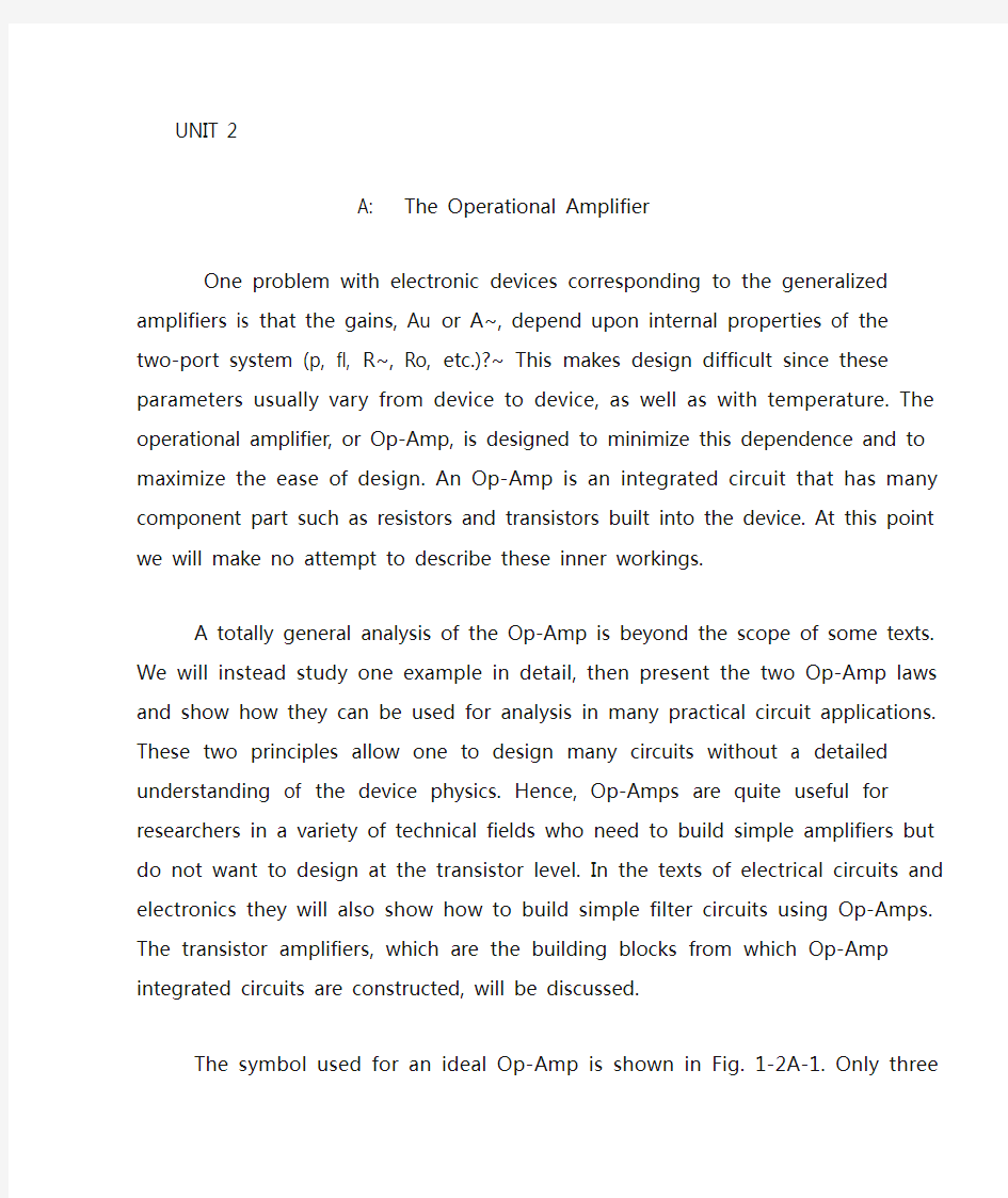
The symbol used for an ideal Op-Amp is shown in Fig. 1-2A-1. Only three connections are shown: the positive and negative inputs, and the output. Not shown are other connections necessary to run the Op-Amp such as its attachments to power supplies and to ground potential. The latter connections are necessary to use the Op-Amp in a practical circuit but are not necessary when considering the ideal 0p-Amp applications we study in this chapter. The voltages
at the two inputs and the output will be
represented by the symbols U+, U-, and Uo. Each is measured with respect t~ ground potential. Operational amplifiers are differential devices. By this we mean that the output voltage with respect to ground is given by the expression
Uo =A(U+ -U-) (1-2A-l) where A is the gain of the Op-Amp and U+ and U - the voltages at inputs. In other words, the output voltage is A times the difference in potential between the two inputs.
Integrated circuit technology allows construction of many amplifier circuits on a single composite "chip" of semiconductor material. One key to the success of an operational amplifier is the "cascading" of a number of transistor amplifiers to create a very large total gain. That is, the number A in Eq. (1-2A-1) can be on the order of 100,000 or more. (For example, cascading of five transistor amplifiers, each with a gain of 10, would yield this value for A.) A second important factor is that these circuits can be built in such a way that the current flow into each of the inputs is very small. A third important design feature is that the output resistance of the operational amplifier (Ro) is very small. This in turn means that the output of the device acts like an ideal voltage source.
We now can analyze the particular amplifier circuit given in Fig. 1-2A-2 using these characteristics. First, we note that the voltage at the positive input, U +, is equal to the source voltage, U + = Us. Various currents are defined in part b of the figure. Applying KVL around the outer loop in Fig. 1-2A-2b and remembering that the output voltage, Uo, is measured with respect to ground, we have
-I1R1-I2R2+U0=0(1-2A-2)
Since the Op-Amp is constructed in such a way that no current flows into either the positive or negative input, I- =0. KCL at the negative input terminal then yields
I1 = I2
Using Eq. (1-2A-2) and setting I1 =I2 =I,
U0=(R1+R2)I(1-2A-3)
We may use Ohm's law to find the voltage at the negative input, U-, noting the assumed current direction and the fact that ground potential is zero volts:
(U--0)/ R1=I
So, U-=IR1
and from Eq. (1-2A-3), U- =[R1/(R1+R2)] U0
Since we now have expressions for U+ and U-, Eq. (1-2A-l) may be used to calculate the output voltage,
U 0 = A(U+-U-)=A[U
S
-R
1
U
/(R
1
+R
2
)]
Gathering terms,
U0 =[1+AR1/(R1+R2)]= AU S(1-2A-4) and finally,
A U = U0/U S= A(R1+R2)/( R1+R2+AR1) (1-2A-5a) This is the gain factor for the circuit. If A is a very large number, large enough that AR~ >> (R1+R2),the denominator of this fraction is dominated by the AR~ term. The factor A, which is in both the numerator and denominator, then cancels out and the gain is given by the expression
A U =(R1+R2)/ R1(1-2A-5b) This shows that if A is very large, then the gain of the circuit is independent of the exact value of A and can be controlled by the choice of R1and R2. This is one of the key features of Op-Amp design the action of the circuit on signals depends only upon the external elements which can be easily varied by the designer and which do not depend upon the detailed character of the Op-Amp itself. Note that if A=100 000 and (R1 +R2)/R1=10, the price we have paid for this advantage is that we have used a device with a voltage gain of 100 000 to produce an amplifier with a gain of 10. In some sense, by using an Op-Amp we trade off "power" for "control."
A similar mathematical analysis can be made on any Op-Amp circuit, but this is
cumbersome and there are some very useful shortcuts that involve application of the two laws of Op-Amps which we now present.
1) The first law states that in normal Op-Amp circuits we may assume that the voltage difference between the input terminals is zero, that is,
U+ =U-
2) The second law states that in normal Op-Amp circuits both of the input currents may be assumed to be zero:
I+ =I- =0
The first law is due to the large value of the intrinsic gain A. For example, if the output of an Op- Amp is IV and A= 100 000, then ( U+ - U- )= 10-SV. This is such a small number that it can often be ignored, and we set U+ = U-. The second law comes from the construction of the circuitry inside the Op-Amp which is such that almost no current flows into either of the two inputs.
B: Transistors
Put very simply a semiconductor material is one which can be 'doped' to produce a predominance of electrons or mobile negative charges (N-type); or 'holes' or positive charges (P- type). A single crystal of germanium or silicon treated with both N-type dope and P-type dope forms a semiconductor diode, with the working characteristics described. Transistors are formed in a similar way but like two diodes back-to-back with a common middle layer doped in the opposite way to the two end layers, thus the middle layer is much thinner than the two end layers or zones.
Two configurations are obviously possible, PNP or NPN (Fig. 1-2B-l). These descriptions are used to describe the two basic types of transistors. Because a transistor contains elements with two different polarities (i.e., 'P' and 'N' zones), it is referred to as a bipolar device, or bipolar transistor.
A transistor thus has three elements with three leads connecting to these elements. To operate in a working circuit it is connected with two external voltage or polarities. One external voltage is working effectively as a diode. A transistor will, in fact, work as a diode by using just this connection and forgetting about the top half. An example is the substitution of a transistor for a diode as the detector in a simple radio. It will work just as well as a diode as it is working as a diode in this case.
The diode circuit can be given forward or reverse bias. Connected with forward bias, as in Fig.l-2B-2, drawn for a PNP transistor, current will flow from P to the bottom N. If a second voltage is applied to the top and bottom sections of the transistor, with the same polarity applied to the bottom, the electrons already flowing through the bottom N section will promote
a
flow of current through the transistor bottom-to-top.
By controlling the degree of doping in the different layers of the transistor during manufacture, this ability to conduct current through the second circuit through a resistor can be very marked. Effectively, when the bottom half is forward biased, the bottom section acts as a generous source of free electrons (and because it emits electrons it is called the emitter). These are collected readily by the top half, which is consequently called the collector, but the actual amount of current which flows through this particular circuit is controlled by the bias applied at the center layer, which is called the base.
Effectively, therefore, there are two separate 'working' circuits when a transistor is working with correctly connected polarities (Fig. 1-2B-3). One is the loop formed by the bias voltage supply encompassing the emitter and base. This is called the base circuit or input circuit. The second is the circuit formed by the collector voltage supply and all three elements of the transistor. This is called the collector circuit or output circuit. (Note: this description applies only when the emitter connection is common to both circuits ~ known as common emitter configuration.) This is the most widely used way of connecting transistors, but there are, of course, two other alternative configurations -- common base and common emitter. But, the same principles apply in the working of the transistor in each case.
The particular advantage offered by this circuit is that a relatively small base current can control and instigate a very much larger collector current (or, more correctly, a small input power is capable of producing a much larger output power). In other words, the transistor works as an amplifier.
With this mode of working the base-emitter circuit is the input side; and the emitter through base to collector circuit the output side. Although these have a common path through base and emitter, the two circuits are effectively separated by the fact that as far as polarity of the base circuit is concerned, the base and upper half of the transistor are connected as a reverse biased diode. Hence there is no current flow from the base circuit into the collector circuit.
For the circuit to work, of course, polarities of both the base and collector circuits have to be correct (forward bias applied to the base circuit, and the collector supply connected so that the polarity of the common element (the emitter) is the same from both voltage sources). This also means that the polarity of the voltages must be correct for the type of transistor. In the case of a PNP transistor as described, the emitter voltage must be positive. It follows that both the base and collector are negatively connected with respect to the emitter. The symbol for a PNP transistor has an arrow on the emitter indicating the direction of current flow, always towards the base. ('P' for positive, with a PNP transistor).
In the case of an NPN transistor, exactly the same working principles apply but the polarities of both supplies are reversed (Fig. 1-2B-4). That is to say, the emitter is always made negative
relative to base and collector ('N' for negative in the case
of an NPN transistor). This is also inferred by the reverse direction of the arrow on the emitter in
the symbol for an NPN transistor, i.e., current flow away from the base.
While transistors are made in thousands of different types, the number of shapes in which they are produced is more limited and more or less standardized in a simple code -- TO (Transistor Outline) followed by a number.
TO1 is the original transistor shape a cylindrical 'can' with the three leads emerging in triangular pattern from the bottom. Looking at the base, the upper lead in the 'triangle' is the base, the one to the fight (marked by a color spot) the collector and the one to the left the emitter.[2] The collector lead may also be more widely spaced from the base lead than the emitter lead.
In other TO shapes the three leads may emerge in similar triangular pattern (but not necessarily with the same positions for base, collector and emitter), or in-line. Just to confuse the issue there are also sub-types of the same TO number shape with different lead designations. The TO92, for example, has three leads emerging in line parallel to a flat side on an otherwise circular 'can' reading 1,2,3 from top to bottom with the flat side to the right looking at the base.
With TO92 sub-type a (TO92a): 1=emitter
2=collector
3=base
With TO92 sub-type b (TO92b): 1=emitter
2=base
3=collector
To complicate things further, some transistors may have only two emerging leads (the third being connected to the case internally); and some transistor outline shapes are found with more than three leads emerging from the base. These, in fact, are integrated circuits (ICs), packaged in the same outline shape as a transistor. More complex ICs are packaged in quite different form, e.g., flat packages.
Power transistors are easily identified by shape~ They are metal cased with an elongated bottom with two mounting holes. There will only be two leads (the emitter and base) and these will normally be marked. The collector is connected internally to the can, and so connection to the collector is via one of the mounting bolts or bottom of the can.
A 运算放大器
对应于像广义放大器这样的电子装置,存在的一个问题就是它们的增益A
U
或A
I,它们取决于双端口系统(μ、β、R
i
、R
等)的内部特性。器件之间参数的分
散性和温度漂移给设计工作增加了难度。设计运算放大器或Op-Amp的目的就是
使它尽可能的减少对其内部参数的依赖性、最大程度地简化设计工作。运算放大器是一个集成电路,在它内部有许多电阻、晶体管等元件。就此而言,我们不再描述这些元件的内部工作原理。
运算放大器的全面综合分析超越了某些教科书的范围。在这里我们将详细研究一个例子,然后给出两个运算放大器定律并说明在许多实用电路中怎样使用这两个定律来进行分析。这两个定律可允许一个人在没有详细了解运算放大器物理特性的情况下设计各种电路。因此,运算放大器对于在不同技术领域中需要使用简单放大器而不是在晶体管级做设计的研究人员来说是非常有用的。在电路和电子学教科书中,也说明了如何用运算放大器建立简单的滤波电路。作为构建运算放大器集成电路的积木—晶体管,将在下篇课文中进行讨论。
理想运算放大器的符号如图1-2A-1所示。图中只给出三个管脚:正输入、负输入和输出。让运算放大器正常运行所必需的其它一些管脚,诸如电源管脚、接零管脚等并未画出。在实际电路中使用运算放大器时,后者是必要的,但在本文中讨论理想的运算放大器的应用时则不必考虑后者。两个输入电压和输出电压用符号U+、U-和U
表示。每一个电压均指的是相对于接零管脚的电位。运算放大器是差分装置。差分的意思是:相对于接零管脚的输出电压可由下式表示
U
=A(U+-U-)
(1-2A-1)
式中 A 是运算放大器的增益,U+和U-是输入电压。换句话说,输出电压是A乘以两输入间的电位差。
集成电路技术使得在非常小的一块半导体材料的复合“芯片”上可以安装许多放大器电路。运算放大器成功的一个关键就是许多晶体管放大器“串联”以产生非常大的整体增益。也就是说,等式(1-2A-1)中的数A约为100,000或更多(例如,五个晶体管放大器串联,每一个的增益为10,那么将会得到此数值的A)。第二个重要因素是这些电路是按照流入每一个输入的电流都很小这样的原则来
设计制作的。第三个重要的设计特点就是运算放大器的输出阻抗(R
)非常小。也就是说运算放大器的输出是一个理想的电压源。
我们现在利用这些特性就可以分析图1-2A-2所示的特殊放大器电路了。首
先,注意到在正极输入的电压U +等于电源电压,即U+ =U
S
。各个电流定义如图
1-2A-2中的b图所示。对图 1-2A-2b的外回路应用基尔霍夫定律,注意输出电
压U
指的是它与接零管脚之间的电位,我们就可得到
-I
1R
1
-I
2
R
2
+U
=0
(1-2A-2)
因为运算放大器是按照没有电流流入正输入端和负输入端的原则制作的,即
I- =0。那么对负输入端利用基尔霍夫定律可得I
1 = I
2
,
利用等式(1-2A-2) ,并设 I
1 =I
2
=I,
U 0 = (R
1
+R
2
) I
(1-2A-3)
根据电流参考方向和接零管脚电位为零伏特的事实,利用欧姆定律,可得负极输入电压U-: (U--0)/ R
1
=I
因此U-=IR
1,并由式 (1-2A-3)可得: U- =[R
1
/(R
1
+R
2
)] U
因为现在已有了U+和U-的表达式,所以式(1-2A-1)可用于计算输出电压,
U 0 = A(U+-U-)=A[U
S
-R
1
U
/(R
1
+R
2
)]
综合上述等式,可得: U
0 =[1+AR
1
/(R
1
+R
2
)]= AU
S
(1-2A-4)
最后可得: A
U = U
/U
S
= A(R
1
+R
2
)/( R
1
+R
2
+AR
1
)
(1-2A-5a)
这是电路的增益系数。如果A 是一个非常大的数,大到足够使AR
1 >> (R
1
+R
2
),
那么分式的分母主要由AR
1
项决定,存在于分子和分母的系数A 就可对消,增益
可用下式表示这表明, A
U =(R
1
+R
2
)/ R
1
(1-2A-5b)
如果A 非常大,那么电路的增益与A 的精确值无关并能够通过R
1和R
2
的选择来
控制。这是运算放大器设计的重要特征之----在信号作用下,电路的动作仅取决于能够容易被设计者改变的外部元件,而不取决于运算放大器本身的细节特性。
注意,如果A=100,000,而(R
1 +R
2
) /R
1
=10,那么为此优点而付出的代价是用
一个具有100,000倍电压增益的器件产生一个具有10倍增益的放大器。从某种意义上说,使用运算放大器是以“能量”为代价来换取“控制”。
对各种运算放大器电路都可作类似的数学分析,但是这比较麻烦,并且存在一些非常有用的捷径,其涉及目前我们提出的运算放大器两个定律应用。
1) 第一个定律指出:在一般运算放大器电路中,可以假设输入端间的电压为零,也就是说,U+ =U-
2) 第二个定律指出:在一般运算放大器电路中,两个输入电流可被假定为零: I+ =I- =0
第一个定律是因为内在增益A的值很大。例,如果运算放大器的输出是1V,并且A=100,000, 那么(U+ = U-)=10-5 V这是一个非常小、可以忽略的数,因此可设
U+ = U-。第二个定律来自于运算放大器的内部电路结构,此结构使得基本上没有电流流入任何一个输入端。
B 晶体管
简单地说,半导体是这样一种物质,它能够通过“掺杂”来产生多余的电子,又称自由电子(N型);或者产生“空穴”,又称正电荷(P型)。由N型掺杂和P型掺杂处理的锗或硅的单晶体可形成半导体二极管,它具有我们描述过的工作特性。晶体管以类似的方式形成,就象带有公共中间层、背靠背的两个二极管,公共中间层是以对等的方式向两个边缘层渗入而得,因此中间层比两个边缘层或边缘区要薄的多。
PNP 或 NPN (图 1-2B-1)这两种结构显然是可能的。PNP或NPN被用于描述晶体管的两个基本类型。因为晶体管包含两个不同极性的区域(例如“P”区和“N”区),所以晶体管被叫作双向器件,或双向晶体管。
一个晶体管有三个区域,并从这三个区域引出三个管脚。要使工作电路运行,晶体管需与两个外部电压或极性连接。其中一个外部电压工作方式类似于二极管。事实上,保留这个外部电压并去掉上半部分,晶体管将会象二极管一样工作。例如在简易收音机中用晶体管代替二极管作为检波器。在这种情况下,其所起的作用和二极管所起的作用一模一样。
可以给二极管电路加正向偏置电压或反向偏置电压。在加正向偏置电压的情况下,如图1-2B-2所示的PNP 晶体管,电流从底部的P极流到中间的N极。如果第二个电压被加到晶体管的顶部和底部两个极之间,并且底部电压极性相同,那么,流过中间层N区的电子将激发出从晶体管底部到顶部流过的电流。
在生产晶体管的过程中,通过控制不同层的掺杂度,经过负载电阻流过第二个电路电流的导电能力非常显著。实际上,当晶体管下半部为正向偏置时,底部的P区就像一个取之不竭的自由电子源(因为底部的P区发射电子,所以它被称为发射极)。这些电子被顶部P区接收,因此它被称为集电极,但是流过这个特定电路实际电流的大小由加到中间层的偏置电压控制,所以中间层被称为基极。
因此,当晶体管外加电压接连正确(图1-2B-3)后工作时,实际上存在两个独立的“工作”电路。一个是由偏置电压源、发射极和基极形成的回路,它被称为基极电路或输入电路;第二个是由集电极电压源和晶体管的三个区共同形成的电路,它被称为集电极电路或输出电路。(注意:本定义仅适用于发射极是两个电路的公共端时----被称为共发射极连接。)这是晶体管最常见的连接方式,但是,当然也存在其它两种连接方法----共基极连接和共集电极连接。但是,在每一种情况下晶体管的工作原理是相同的。
本电路的突出优点是相对小的基极电流能控制和激发出一个比它大得多的集电极电流(或更恰当地说,一个小的输入功率能够产生一个比它大得多的输出功率)。换句话说,晶体管的作用相当于一个放大器。
在这种工作方式中,基极-发射极电路是输入侧;通过基极的发射极和集电极电路是输出侧。虽然基极和发射极是公共路径,但这两个电路实际上是独立的,就基极电路的极性而言,基极和晶体管的集电极之间相当于一个反向偏置二极管,因此没有电流从基极电路流到集电极电路。
要让电路正常工作,当然,加在基极电路和集电极电路的电压极性必须正确(基极电路加正向偏置电压,集电极电源的连接要保证公共端(发射极)的极性与两个电压源的极性相同)。这也就是说电压极性必须和晶体管的类型相匹配。在上述的PNP型晶体管中,发射极电压必须为正。因此,基极和集电极相对于发射极的极性为负。PNP 型晶体管的符号在发射极上有一个指示电流方向的箭头,总是指向基极。(在PNP型晶体管中,“P”代表正)。
在NPN型晶体管中,工作原理完全相同,但是两个电源的极性正好相反(图1-2B-4)。也就是说,发射极相对于基极和集电极来说极性总是负的(在NPN
型晶体管中,“N”代表负)。这一点也可以从NPN型晶体管符号中发射极上相反方向的箭头看出来,即,电流从基极流出。
尽管现在生产的晶体管有上千种不同的型号,但晶体管各种外壳形状的数量相对有限,并尽量用一种简单码----TO(晶体管外形)后跟一个数字为统一标准。
TO1是一种最早的晶体管外壳----即一个在底部带有三个引脚的圆柱体“外罩”,这三个引脚在底部形成三角状。观看底部时,“三角形”上面的管脚是基极,其右面的管脚(由一个彩色点标出)为集电极,其左面的管脚为发射极。集电极引脚到基集引脚的间距也许比发射极到基集引脚的间距要大。
在其它TO外壳中,三个引脚可能有类似的三角形形状(但是基极、集电极和发射极的位置不一定相同),或三个引脚排成一条直线。使人容易搞乱的问题是同一TO号码的子系列产品其管脚位置是不一样的。例如,TO92 的三个管脚排成一条直线,这条直线与半圆型“外罩”的切面平行,观看TO92的底部时,将切面冲右,从上往下读,管脚的排序为1,2,3。
对于TO92子系列 a (TO92a): 1=发射极
2=集电极
3=基极
对于TO92子系列 b (TO92b): 1=发射极
2=基极
3=集电极
更容易使人搞乱的是一些晶体管只有两个管脚(第三个管脚已在里边和外壳连接);一些和晶体管的外形很像的外壳底部有三个以上的管脚。实际上,这些都是集成电路(ICs),用和晶体管相同的外壳包装的,只是看起来像晶体管。更复杂的集成电路(ICs)用不同形状的外壳包装,例如平面包装。
根据外壳形状非常容易识别功率晶体管。它们是金属外壳,带有延长的底部平面,底部平面上还有两个安装孔。功率晶体管只有两个管脚(发射极和基极),通常会标明。集电极在内部被连接到外壳上,因此,与集电极的连接要通过一个装配螺栓或外壳底面。
《自动化专业英语》中英文翻译-中文部分
第二部分 控制理论 第1章 1.1控制系统的引入 人类控制自然力量的设计促进人类历史的发展,我们已经广泛的能利用这种量进行在人类本身力量之外的物理进程?在充满活力的20世纪中,控制系统工程的发展已经使得很多梦想成为了现实?控制系统工程队我们取得的成就贡献巨大?回首过去,控制系统工程主要的贡献在机器人,航天驾驶系统包括成功的实现航天器的软着陆,航空飞机自动驾驶与自动控制,船舶与潜水艇控制系统,水翼船?气垫船?高速铁路自动控制系统,现代铁路控制系统? 以上这些类型的控制控制系统和日常生活联系紧密,控制系统是一系列相关的原件在系统运行的基础上相互关联的构成的,此外控制系统存在无人状态下的运行,如飞机自控驾驶,汽车的巡航控制系统?对于控制系统,特别是工业控制系统,我们通常面对的是一系列的器件,自动控制是一个复合型的学科?控制工程师的工作需要具有力学,电子学,机械电子,流体力学,结构学,无料的各方面的知识?计算机在控制策略的执行中具有广泛的应用,并且控制工程的需求带动了信息技术的与软件工程的发展? 通常控制系统的范畴包括开环控制系统与闭环控制系统,两种系统的区别在于是否在系统中加入了闭环反馈装置? 开环控制系统 开环控制系统控制硬件形式很简单,图2.1描述了一个单容液位控制系统, 图2.1单容液位控制系统 我们的控制目标是保持容器的液位h 在水流出流量V 1变化的情况下保持在一定 可接受的范围内,可以通过调节入口流量V 2实现?这个系统不是精确的系统,本系 统无法精确地检测输出流量V 2,输入流量V 1以及容器液位高度?图2.2描述了这 个系统存在的输入(期望的液位)与输出(实际液位)之间的简单关系, 图2.2液位控制系统框图 这种信号流之间的物理关系的描述称为框图?箭头用来描述输入进入系统,以及
农业产业化外文翻译文献
农业产业化外文翻译文献(文档含中英文对照即英文原文和中文翻译)
农业产业化:从农场到交易市场 Mark R. Edwards and Clifford. J. Shultz 摘要 农业产业化就是农业以市场需求为导向,有效的满足客户以及市场要求的一系列的链条。这种变革需要一个更广泛的概念化和更准确的定义,传达一个致力于创造价值和可持续利用食物,纤维,可再生资源的更有活力,系统性,综合性和纪律性的系统。我们讨论的力量,推动这一转移到市场,提供了新的和更具有代表性农业产业化的定义,提供模型以说明一些最引人注目的趋势,并阐明这些模型关键因素和影响。 关键词:农业产业化的定义,概念模型,市场为中心,市场体系
1 绪论 农业产业化在1955年开始作为一个独特的研究领域,当时约翰.戴维斯将它定义为:农业产业化是以农场生产为中心,然后商品化。这个定义当时是最适当的,那是农业行动的重点是最大限度地生产食物和纤维。戴维斯和高德博格用新鲜的见解,将农业产业化定义为:制造和分销农场用品:在该农场生产经营、储存、加工、分销所有的农产品的商品和物品所涉及的所有业务的总和。类似的定义也有其他的人提出,如唐尼和埃里克森:农业产业化,包括所有这些业务和管理活动由公司提供投入到农业部门,生产农产品,运输,金融,处理农产品的全部过程。 这些传统的定义,随着时间的推移,对农场或生产的单位所反映农业产业化的焦点,如农业交易中心已数十年之久。今天,一个就业散点图显示,虽然超过百分之三十的就业机会农业产业化提供的,少于百分之一的人直接参与农场生产。农业产业化已不再是以农场为中心。二十一世纪农业产业化包含了更广泛的一系列行动,主要是外围行动,包括以市场为导向的可持续利用食物,纤维,和可再生资源。
英文翻译 机械自动化类
Mechatronics Electrical machinery and electronics, also known as the integration of science, English as Mechatronics, it is by English mechanics of the first half of Mechanics and Electronics of the latter part of a combination of Electronics. Mechatronics 1971, first appeared in Japanese magazine, "Machine Design" on the supplement, with the mechanical-electrical integration of the rapid development of technology, electromechanical integration, the concept was widely accepted and we have universal application. With the rapid development of computer technology and extensive application of mechatronics technology unprecedented development. Mechatronics present technology, mechanical and micro-electronics technology is closely a set of technologies, the development of his machine has been cold humane, intelligent. Specific mechanical and electrical integration technologies, including the following: (1) mechanical engineering machinery and technology is the basis of mechatronics, mechanical technology, focused on how to adapt to mechanical and electrical integration technologies, the use of other high and new technology to update the concept, the realization of the structure, materials, the performance changes to meet the needs to reduce weight, reduce the size and improve accuracy, increase the stiffness and improving the performance requirements. Mechatronic systems in the manufacturing process, the classical theory and technology of mechanical computer-aided technology should help, while the use of artificial intelligence and expert systems, the formation of a new generation of mechanical manufacturing technology. (2) Computer and Information Technology Which information exchange, access, computing, judge and decision-making, artificial intelligence techniques, expert system technology, neural networks are computer information processing technology. (3) System Technology System technology that is the concept of the overall application of related technology organizations, from the perspective of the overall objectives and systems will be interconnected into the overall number of functional units, system interface technology is an important aspect of technology, it is an organic part of the realization of system guarantee connectivity.
电气工程及其自动化专业_外文文献_英文文献_外文翻译_plc方面
1、 外文原文 A: Fundamentals of Single-chip Microcomputer Th e si ng le -c hi p m ic ro co mp ut er i s t he c ul mi na ti on of both t h e de ve lo pm en t o f t he d ig it al co m pu te r an d th e i n te gr at ed c i rc ui t a rg ua bl y t h e to w m os t s ig ni f ic an t i nv en ti on s o f t he 20th c e nt ur y [1]. Th es e t ow ty pe s of ar ch it ec tu re a re fo un d i n s in g le -ch i p m i cr oc om pu te r. So m e em pl oy t he spl i t pr og ra m/da ta m e mo ry o f th e H a rv ar d ar ch it ect u re , sh ow n in Fi g.3-5A -1, o th ers fo ll ow t he p h il os op hy , wi del y a da pt ed f or ge n er al -p ur po se co m pu te rs a nd m i cr op ro ce ss o r s, o f ma ki ng n o log i ca l di st in ct ion be tw ee n p r og ra m an d d at a m e mo ry a s i n t he P r in ce to n ar ch ite c tu re , sh ow n i n F ig.3-5A-2. In g en er al te r ms a s in gl e -chi p m ic ro co mp ut er i s c h ar ac te ri ze d b y t h e i nc or po ra ti on o f a ll t he un it s of a co mp uter i n to a s in gl e d ev i ce , as s ho wn in Fi g3-5A -3. Fig.3-5A-1 A Harvard type Program memory Data memory CPU Input& Output unit memory CPU Input& Output unit
农业产业化组织的营销策略分析-外文翻译
外文翻译 原文 Title:Agricultural Industrialization Organization of Marketing Strategy Analysis Material source:2010 International Conference on Industry Engineering and Management Author:Zhao Yanhong, Ren Aihua Abstraet:Agricultural industrialization is the development direction of world agriculture, it is also the main form of the agricultural operation in developed countries. Vigorously develop the industrialization of agriculture is to enhance the competitiveness of China’s agricultu re is an effective means of marketing innovation in agriculture. It is related to the industrialization of agriculture an important factor in business success. In this paper, product, place, promotion, three organizations, the face of the industrialization of agriculture marketing innovation of the corresponding development proposals. Keywords:Product;Channel Innovation;Promotion 1 Introduction Although China has already established a number of agricultural industrialization organization, but very few successful cases, reason, the product can not sell that influence their development, an important factor. At present the industrialization of agriculture organizations in product development, sales channels and marketing methods. There are many ways to solve urgent problems, we can say, marketing has become a bottleneck restricting development of the organization. In this Paper, the development of marketing concept, mainly based on the content of the theory of 4P, from development to meet consumer demand for products. Innovation in the channel, flexible use of marketing mix and so the organization seeking to promote the industrialization of agriculture marketing of innovative measures. 2 Development of Products to Meet Consumer Demand 4C theory holds that companies should give top priority to the pursuit of customer satisfaction, then theagricultural industry of the organization must first develop a customer satisfaction products. Marketing believes that demand for the
模具毕业设计外文翻译(英文+译文)
Injection Molding The basic concept of injection molding revolves around the ability of a thermoplastic material to be softened by heat and to harden when cooled .In most operations ,granular material (the plastic resin) is fed into one end of the cylinder (usually through a feeding device known as a hopper ),heated, and softened(plasticized or plasticized),forced out the other end of the cylinder, while it is still in the form of a melt, through a nozzle into a relatively cool mold held closed under pressure.Here,the melt cools and hardens until fully set-up. The mold is then opened, the piece ejected, and the sequence repeated. Thus, the significant elements of an injection molding machine become: 1) the way in which the melt is plasticized (softened) and forced into the mold (called the injection unit); 2) the system for opening the mold and closing it under pressure (called the clamping unit);3) the type of mold used;4) the machine controls. The part of an injection-molding machine, which converts a plastic material from a sold phase to homogeneous seni-liguid phase by raising its temperature .This unit maintains the material at a present temperature and force it through the injection unit nozzle into a mold .The plunger is a combination of the injection and plasticizing device in which a heating chamber is mounted between the plunger and mold. This chamber heats the plastic material by conduction .The plunger, on each stroke; pushes unbelted plastic material into the chamber, which in turn forces plastic melt at the front of the chamber out through the nozzle The part of an injection molding machine in which the mold is mounted, and which provides the motion and force to open and close the mold and to hold the mold close with force during injection .This unit can also provide other features necessary for the effective functioning of the molding operation .Moving
自动化外文翻译
景德镇陶瓷学院 毕业设计(论文)有关外文翻 译 院系:机械电子工程学院 专业:自动化 姓名:肖骞 学号: 201010320116 指导教师:万军 完成时间: 2014.5.8 说明
1、将与课题有关的专业外文翻译成中文是毕业设计(论文)中的一个不可缺少的环节。此环节是培养学生阅读专业外文和检验学生专业外文阅读能力的一个重要环节。通过此环节进一步提高学生阅读专业外文的能力以及使用外文资料为毕业设计服务,并为今后科研工作打下扎实的基础。 2、要求学生查阅与课题相关的外文文献3篇以上作为课题参考文献,并将其中1篇(不少于3000字)的外文翻译成中文。中文的排版按后面格式进行填写。外文内容是否与课题有关由指导教师把关,外文原文附在后面。 3、指导教师应将此外文翻译格式文件电子版拷给所指导的学生,统一按照此排版格式进行填写,完成后打印出来。 4、请将封面、译文与外文原文装订成册。 5、此环节在开题后毕业设计完成前完成。 6、指导教师应从查阅的外文文献与课题紧密相关性、翻译的准确性、是否通顺以及格式是否规范等方面去进行评价。 指导教师评语: 签名: 年月日
TMS320LF2407, TMS320LF2406, TMS320LF2402 TMS320LC2406, TMS320LC2404, MS320LC2402 DSP CONTROLLERS The TMS320LF240x and TMS320LC240x devices, new members of the ‘24x family of digital signal processor (DSP) controllers, are part of the C2000 platform of fixed-point DSPs. The ‘240x devices offer the enhanced TMS320 architectural design of the ‘C2xx core CPU for low-cost, low-power, high-performance processing capabilities. Several advanced peripherals, optimized for digital motor and motion control applications, have been integrated to provide a true single chip DSP controller. While code-compatible with the existing ‘24x DSP controller devices, the ‘240x offers increased processing performance (30 MIPS) and a higher level of peripheral integration. See the TMS320x240x device summary section for device-specific features. The ‘240x family offers an array of memory sizes and different peripherals tailored to meet the specific price/performance points required by various applications. Flash-based devices of up to 32K words offer a reprogrammable solution useful for: ◆Applications requiring field programmability upgrades. ◆Development and initial prototyping of applications that migrate to ROM-based devices. Flash devices and corresponding ROM devices are fully pin-to-pin compatible. Note that flash-based devices contain a 256-word boot ROM to facilitate in-circuit programming. All ‘240x devices offer at least one event manager module which has been optimized for digital motor control and power conversion applications. Capabilities of this module include centered- and/or edge-aligned PWM generation, programmable deadband to prevent shoot-through faults, and synchronized analog-to-digital conversion. Devices with dual event managers enable multiple motor and/or converter
电气自动化专业毕业论文英文翻译
电厂蒸汽动力的基础和使用 1.1 为何需要了解蒸汽 对于目前为止最大的发电工业部门来说, 蒸汽动力是最为基础性的。 若没有蒸汽动力, 社会的样子将会变得和现在大为不同。我们将不得已的去依靠水力发电厂、风车、电池、太阳能蓄电池和燃料电池,这些方法只能为我们平日用电提供很小的一部分。 蒸汽是很重要的,产生和使用蒸汽的安全与效率取决于怎样控制和应用仪表,在术语中通常被简写成C&I(控制和仪表 。此书旨在在发电厂的工程规程和电子学、仪器仪表以 及控制工程之间架设一座桥梁。 作为开篇,我将在本章大体描述由水到蒸汽的形态变化,然后将叙述蒸汽产生和使用的基本原则的概述。这看似简单的课题实际上却极为复杂。这里, 我们有必要做一个概述:这本书不是内容详尽的论文,有的时候甚至会掩盖一些细节, 而这些细节将会使热力学家 和燃烧物理学家都为之一震。但我们应该了解,这本书的目的是为了使控制仪表工程师充 分理解这一课题,从而可以安全的处理实用控制系统设计、运作、维护等方面的问题。1.2沸腾:水到蒸汽的状态变化 当水被加热时,其温度变化能通过某种途径被察觉(例如用温度计 。通过这种方式 得到的热量因为在某时水开始沸腾时其效果可被察觉,因而被称为感热。 然而,我们还需要更深的了解。“沸腾”究竟是什么含义?在深入了解之前,我们必须考虑到物质的三种状态:固态,液态,气态。 (当气体中的原子被电离时所产生的等离子气体经常被认为是物质的第四种状态, 但在实际应用中, 只需考虑以上三种状态固态,
物质由分子通过分子间的吸引力紧紧地靠在一起。当物质吸收热量,分子的能量升级并且 使得分子之间的间隙增大。当越来越多的能量被吸收,这种效果就会加剧,粒子之间相互脱离。这种由固态到液态的状态变化通常被称之为熔化。 当液体吸收了更多的热量时,一些分子获得了足够多的能量而从表面脱离,这个过程 被称为蒸发(凭此洒在地面的水会逐渐的消失在蒸发的过程中,一些分子是在相当低的 温度下脱离的,然而随着温度的上升,分子更加迅速的脱离,并且在某一温度上液体内部 变得非常剧烈,大量的气泡向液体表面升起。在这时我们称液体开始沸腾。这个过程是变为蒸汽的过程,也就是液体处于汽化状态。 让我们试想大量的水装在一个敞开的容器内。液体表面的空气对液体施加了一定的压 力,随着液体温度的上升,便会有足够的能量使得表面的分子挣脱出去,水这时开始改变 自身的状态,变成蒸汽。在此条件下获得更多的热量将不会引起温度上的明显变化。所增 加的能量只是被用来改变液体的状态。它的效用不能用温度计测量出来,但是它仍然发生 着。正因为如此,它被称为是潜在的,而不是可认知的热量。使这一现象发生的温度被称为是沸点。在常温常压下,水的沸点为100摄氏度。 如果液体表面的压力上升, 需要更多的能量才可以使得水变为蒸汽的状态。 换句话说, 必须使得温度更高才可以使它沸腾。总而言之,如果大气压力比正常值升高百分之十,水必须被加热到一百零二度才可以使之沸腾。
美国农业合作社与农业产业化外文文献翻译中英文
美国农业合作社与农业产业化外文文献翻译中英文最新 (节选重点翻译) 英文 Managing uncertainty and expectations: The strategic response of U.S. agricultural cooperatives to agricultural industrialization Julie Hogeland Abstract The 20th century industrialization of agriculture confronted U.S. agricultural cooperatives with responding to an event they neither initiated nor drove. Agrarian-influenced cooperatives used two metaphors, “serfdom” and “cooperatives are like a family” to manage uncertainty and influence producer expectations by predicting industrialization's eventual outcome and cooperatives’ producer driven compensation. The serfdom metaphor alluded to industrialization's potential to either bypass family farmers, the cornerstone of the economy according to agrarian ideology, or to transform them into the equivalent of piece-wage labor as contract growers. The “family” metaphor reflects how cooperatives personalized the connection between cooperative and farmer-member to position themselves as the exact opposite of serfdom. Hypotheses advanced by Roessl (2005) and Goel (2013) suggest that intrinsic characteristics of family businesses such as a resistance to change and operating according to a myth of unlimited choice and
模具设计与制造外文翻译
The mold designing and manufacturing The mold is the manufacturing industry important craft foundation, in our country, the mold manufacture belongs to the special purpose equipment manufacturing industry. China although very already starts to make the mold and the use mold, but long-term has not formed the industry. Straight stabs 0 centuries 80's later periods, the Chinese mold industry only then drives into the development speedway. Recent years, not only the state-owned mold enterprise had the very big development, the three investments enterprise, the villages and towns (individual) the mold enterprise's development also rapid quietly. Although the Chinese mold industrial development rapid, but compares with the demand, obviously falls short of demand, its main gap concentrates precisely to, large-scale, is complex, the long life mold domain. As a result of in aspect and so on mold precision, life, manufacture cycle and productivity, China and the international average horizontal and the developed country still had a bigger disparity, therefore, needed massively to import the mold every year . The Chinese mold industry must continue to sharpen the productivity, from now on will have emphatically to the profession internal structure adjustment and the state-of-art enhancement. The structure adjustment aspect, mainly is the enterprise structure to the specialized adjustment, the product structure to center the upscale mold development, to the import and export structure improvement, center the upscale automobile cover mold forming analysis and the structure improvement, the multi-purpose compound mold and the compound processing and the laser technology in the mold design manufacture application, the high-speed cutting, the super finishing and polished the technology, the information direction develops . The recent years, the mold profession structure adjustment and the organizational reform step enlarges, mainly displayed in, large-scale, precise, was complex, the long life, center the upscale mold and the mold standard letter development speed is higher than the common mold product; The plastic mold and the compression casting mold proportion increases; Specialized mold factory quantity and its productivity increase;
自动化外文翻译
电气工程与自动化学院 本科毕业设计专业翻译资料(中文读书报告) 学生姓名:王超杰 专业班级:自动化12-06班 学号:311208002219 2016 年 6 月11 日
原文: Design of Combustible Gas Detection system using Wireless Transmission Technology Shijiazhuang Universities of Economics, Hebei, China zkzhlp@https://www.360docs.net/doc/8a13285965.html, Keywords:TGS813, AT89S52, DS18B20, nRF905, TC35i Abstract.The detection device of combustible gas are designed in the presented work,using wireless transceiver and GSM network.The system realize the wireless transmission of the gas concentration,and also can send alarm information to user’s mobile when an exception occurs. The system consists of two parts: a master and slave. The function of the slave is to collect data, process data and transffer the data to the master.The taskof the master is to receive data and display it by LED. The signal acquisition is completed by sensor TGS813 and A/D converter TLC2543. The wireless transmission is achieved through wireless transceiver nRF905. Since the accuracy of the sensor is affected by the environment,using DS18B20 to achieve temperature compensation. And with wireless communication module TC35i and GSM network platform, we can send the alarm information to user’s mobile promptly. Introduction Gas detection is widely used in petroleum, chemical, metallurgy, family, shopping malls, gas stations and other places. Currently, how to monitor the hazardous gas fast and accurately are the important issues. Although the gas detection technology is relatively mature, but most products has many shortcomings, such as single function, operating complex, bulky, expensive and low sensitivity. Wireless communication technology applied to the gas monitoring field, can resolve the problem of remote monitoring in special environment, such as high temperature, low temperature, toxic gas.and unable to wiring . In the presented work, the combustible gas detectoris fully functional (with wireless transceiver), simple, small size, low cost, and has high sensitivity. The equipment can greatly improve the system's detection capability and accuracy with temperature compensation algorithm, and also can send alarm information to the user's mobile phone promptly through the GSM network. System design The system consists of two parts as shown in Figure 1. Fig. 1 Overall system block diagram