FPGA可编程逻辑器件芯片EP1S30F780I5N中文规格书
FPGA可编程逻辑器件芯片EP1S10F780I7N中文规格书

Figure2–55.Output TIming Diagram in DDR ModeThe Stratix II IOE operates in bidirectional DDR mode by combining theDDR input and DDR output configurations. The negative-edge-clockedOE register holds the OE signal inactive until the falling edge of the clock.This is done to meet DDR SDRAM timing requirements.External RAM InterfacingIn addition to the six I/O registers in each IOE, Stratix II devices also havededicated phase-shift circuitry for interfacing with external memoryinterfaces. Stratix II devices support DDR and DDR2 SDRAM, QDR IISRAM, RLDRAM II, and SDR SDRAM memory interfaces. In everyStratix II device, the I/O banks at the top (banks 3 and 4) and bottom(banks 7 and 8) of the device support DQ and DQS signals with DQ busmodes of ×4, ×8/×9, ×16/×18, or ×32/×36. Table2–14 shows the numberof DQ and DQS buses that are supported per device.Table2–14.DQS & DQ Bus Mode Support(Part 1 of2)Note(1)Device Package Number of×4GroupsNumber of×8/×9 GroupsNumber of×16/×18 GroupsNumber of×32/×36 GroupsEP2S15484-pin FineLine BGA8400 672-pin FineLine BGA18840 EP2S30484-pin FineLine BGA8400 672-pin FineLine BGA18840 EP2S60484-pin FineLine BGA8400 672-pin FineLine BGA188401,020-pin FineLine BGA361884I/O StructureTable 2–15 shows the possible settings for the I/O standards with drive strength control.Open-Drain OutputStratix II devices provide an optional open-drain (equivalent to an open-collector) output for each I/O pin. This open-drain output enables the device to provide system-level control signals (e.g., interrupt and write-enable signals) that can be asserted by any of several devices.Bus HoldEach Stratix II device I/O pin provides an optional bus-hold feature. The bus-hold circuitry can weakly hold the signal on an I/O pin at itslast-driven state. Since the bus-hold feature holds the last-driven state of the pin until the next input signal is present, you do not need an external pull-up or pull-down resistor to hold a signal level when the bus is tri-stated.Table 2–15.Programmable Drive Strength Note (1)I/O StandardI OH / I OL Current Strength Setting (mA) for ColumnI/O PinsI OH / I OL Current Strength Setting (mA) for Row I/OPins3.3-V LVTTL 24, 20, 16, 12, 8, 412, 8, 43.3-V LVCMOS 24, 20, 16, 12, 8, 48, 42.5-V LVTTL/LVCMOS 16, 12, 8, 412, 8, 41.8-V LVTTL/LVCMOS 12, 10, 8, 6, 4, 28, 6, 4, 21.5-V LVCMOS 8, 6, 4, 24, 2SSTL-2 Class I 12, 812, 8SSTL-2 Class II 24, 20, 1616SSTL-18 Class I 12, 10, 8, 6, 410, 8, 6, 4SSTL-18 Class II 20, 18, 16, 8-HSTL-18 Class I 12, 10, 8, 6, 412, 10, 8, 6, 4HSTL-18 Class II 20, 18, 16-HSTL-15 Class I 12, 10, 8, 6, 48, 6, 4HSTL-15 Class II 20, 18, 16-Note to Table 2–15:(1)The Quartus II software default current setting is the maximum setting for each I/O standard.The bus-hold circuitry also pulls undriven pins away from the input threshold voltage where noise can cause unintended high-frequency switching. You can select this feature individually for each I/O pin. The bus-hold output drives no higher than V CCIO to prevent overdriving signals. If the bus-hold feature is enabled, the programmable pull-up option cannot be used. Disable the bus-hold feature when the I/O pin has been configured for differential signals.The bus-hold circuitry uses a resistor with a nominal resistance (R BH) of approximately 7 kΩ to weakly pull the signal level to the last-driven state. See the DC & Switching Characteristics chapter in the Stratix II Device Handbook, Volume 1, for the specific sustaining current driven through this resistor and overdrive current used to identify the next-driven input level. This information is provided for each V CCIO voltage level.The bus-hold circuitry is active only after configuration. When going into user mode, the bus-hold circuit captures the value on the pin present at the end of configuration.Programmable Pull-Up ResistorEach Stratix II device I/O pin provides an optional programmablepull-up resistor during user mode. If you enable this feature for an I/O pin, the pull-up resistor (typically 25 kΩ) weakly holds the output to the V CCIO level of the output pin’s bank.Programmable pull-up resistors are only supported on user I/O pins, and are not supported on dedicated configuration pins, JTAG pins or dedicated clock pins.Advanced I/O Standard SupportStratix II device IOEs support the following I/O standards:■ 3.3-V LVTTL/LVCMOS■ 2.5-V LVTTL/LVCMOS■ 1.8-V LVTTL/LVCMOS■ 1.5-V LVCMOS■ 3.3-V PCI■ 3.3-V PCI-X mode 1■LVDS■LVPECL (on input and output clocks only)■HyperTransport technology■Differential 1.5-V HSTL Class I and II■Differential 1.8-V HSTL Class I and II■Differential SSTL-18 Class I and II■Differential SSTL-2 Class I and IIFor JTAG chains, the TDO pin of the first device drives the TDI pin of the second device in the chain. The V CCSEL input on JTAG input I/O cells (TCK , TMS , TDI , and TRST ) is internally hardwired to GND selecting the 3.3-V/2.5-V input buffer powered by V CCPD . The ideal case is to have the V CCIO of the TDO bank from the first device to match the V CCSEL settings for TDI on the second device, but that may not be possible depending on the application. Table 2–20 contains board design recommendations to ensure proper JTAG chain operation.Table 2–19.Board Design Recommendations for nCEO nCE Input Buffer Power in I/OBank 3Stratix II nCEO V CCIO Voltage Level in I/O Bank 7V C C I O = 3.3 V V C C I O =2.5 V V C C I O =1.8 V V C C I O =1.5 V V C C I O =1.2 V VCCSEL high(V C C I O Bank 3 = 1.5 V)v (1), (2)v (3), (4)v (5)v vVCCSEL high(V C C I O Bank 3 = 1.8 V)v (1), (2)v (3), (4)v vLevel shifter requiredVCCSEL low(nCE Powered by V C C P D = 3.3V)vv (4)v (6)Level shifter required Level shifter requiredNotes to Table 2–19:(1)Input buffer is 3.3-V tolerant.(2)The nCEO output buffer meets V O H (MIN) = 2.4 V .(3)Input buffer is 2.5-V tolerant.(4)The nCEO output buffer meets V OH (MIN) = 2.0 V .(5)Input buffer is 1.8-V tolerant.(6)An external 250-Ω pull-up resistor is not required, but recommended if signal levels on the board are not optimal.Table 2–20.Supported TDO/TDI Voltage Combinations (Part 1 of 2)DeviceTDI InputBuffer Power Stratix II TDO V C C I O Voltage Level in I/O Bank 4VC C I O = 3.3 V V C C I O = 2.5 V V C C I O = 1.8 V V C C I O = 1.5 V V C C I O = 1.2 VStratix IIAlwaysV C C P D (3.3V)v (1)v (2)v (3)Level shifter required Level shifter required。
FPGA可编程逻辑器件芯片EP3C120F780I7中文规格书

Table 55.Configuration Space Offsets Registers User Avalon-MM OffsetsComments Physical function 00x0000Refer to Appendix A for more details of the PF configuration space. This PF is available for x16, x8 and x4 cores.User Avalon-MM Port Configuration Register 0x104068Refer to User Avalon-MM Port Configuration Register (Offset 0x104068) for more details.Debug (DBI) Register 0x104200 to 0x104204Refer to Using the Debug Register Interface Access on page 79 for more details.4.10.2. Configuration Registers Access4.10.2.1. Using Direct User Avalon-MM Interface (Byte Access)Targeting PF Configuration Space RegistersUser application needs to specify the offsets of the targeted PF registers.For example, if the application wants to read the MSI Capability Register of PF0, it will issue a Read with address 0x0050 to target the MSI Capability Structure of PF0.Figure 29.PF Configuration Space Registers Access Timing DiagramHIP reconfig clkHIP reconfig addrHIP reconfig readHIP reconfig readdataHIP reconfig readdatavalid Targeting VSEC RegistersUser application needs to program the VSEC field (0x104068 bit[0]) first. Then all accesses from the user Avalon-MM interface starting at offset 0xD00 will be translated to VSEC configuration space registers.Figure 30.VSEC Registers Access Timing DiagramHIP reconfig clkHIP reconfig addrHIP reconfig writeHIP reconfig writedataHIP reconfig readHIP reconfig waitrequestHIP reconfig readdataHIP reconfig readdatavalid 4.10.2.2. Using the Debug Register Interface AccessDEBUG_DBI_ADDR register is located at user Avalon-MM offsets 0x104204 to0x104207 (corresponding to byte 0 to byte 3). For example, the d_done bit is bit 7 at byte address 0x104207.4.InterfacesUG-20237 | 2021.03.29Send FeedbackTable 56.DEBUG_DBI_ADDR Register NamesBits R/W Descriptions d_done31RO 1: indicates debug DBI read/write access done d_write 30R/W 1: write access0: read accessd_warm_reset 29RO 1: normal operation0: warm reset is on-goingd_vf 28:18R/W Specify the virtual function number .d_vf_select 17R/W To access the virtual function registers, set this bit to one.d_pf 16:14R/W Specify the physical function number .reserved 13:12R/W Reservedd_addr 11:2R/W Specify the DW address for the P-Tile Avalon-MM IP DBI interface.d_shadow_select 1R/W Reserved. Clear this bit for access to standard PCIe configuration registers.d_vsec_select0R/WIf set, this bit allows access to Intel VSEC registers.DEBUG_DBI_DATA register is located at user Avalon-MM offsets 0x104200 to 0x104203 (corresponding to byte 0 to byte 3).Table 57.DEBUG_DBI_DATA RegisterNamesBits R/W Descriptions d_data 31:0R/W Read or write data for the P-Tile Avalon-MM IP register access.To write all 32 bits in a Debug register at a time:1.Use the user_avmm interface to access 0x104200 to 0x104203 to write the data first.2.Use the user_avmm interface to access 0x104204 to 0x104206 to set the address and control bits.3.Use the user_avmm interface to write to 0x104207 to enable the read/write bit (bit[30])e the user_avmm interface to access 0x104207 bit[31] to poll if the write is complete.4.InterfacesUG-20237 | 2021.03.29Send FeedbackFigure 31.DBI Register Write Timing DiagramHIP reconfig clkHIP reconfig addrHIP reconfig writeHIP reconfig writedataHIP reconfig waitrequestHIP reconfig readHIP reconfig readdataHIP reconfig readdatavalid To read all 32 bits in a Debug register at a time:1.Use the user_avmm interface to access 0x104204 to 0x104206 to set the address and control bits.2.Use the user_avmm interface to write to 0x104207 to enable the read bit (bit[30]).3.Use the user_avmm interface to access 0x104207 bit[31] to poll if the read is complete.4.Use the user_avmm interface to access 0x104200 to 0x104203 to read the data Figure 32.DBI Register Read Timing Diagram4.11. PHY Reconfiguration InterfaceThe PHY reconfiguration interface is an optional Avalon-MM slave interface with a 26-bit address and an 8-bit data bus. Use this bus to read the value of PHY registers.Refer to Table 62 on page 90 for details on addresses and bit mappings for the PHY registers that you can access using this interface.These signals are present when you turn on Enable PHY reconfiguration on the Top-Level Settings tab using the parameter editor .Please note that the PHY reconfiguration interface is shared among all the PMA quads.Table 58.PHY Reconfiguration Interface4.InterfacesUG-20237 | 2021.03.29Send Feedback。
FPGA可编程逻辑器件芯片EP3C80F780I7中文规格书

Chapter 1:Stratix III Device Data Sheet: DC and Switching CharacteristicsElectrical CharacteristicsRefer to the figures for “Differential I/O Standards” in “Glossary” for receiver inputand transmitter output waveforms, and for all differential I/O standards (LVDS,mini-LVDS, RSDS). V CC_CLKIN is the power supply for differential column clock inputpins. V CCPD is the power supply for row I/Os and all other column I/Os.Table1–16.Differential SSTL I/O Standard SpecificationsI/O StandardVCCIO(V)VSWING (DC)(V)VX (AC)(V)VSWING(AC)(V)VOX (AC)(V)Min Typ Max Min Max Min Typ Max Min Max Min Typ MaxSSTL-2 CLASS I,II 2.375 2.5 2.6250.3VCCIO+0.6VCCIO/2-0.2—VCCIO/2+0.20.62VCCIO+0.6VCCIO/2-0.15—V CCIO/2 +0.15SSTL-18 CLASS I,II 1.71 1.8 1.890.25VCCIO+0.6VCCIO/2-0.175—VCCIO/2+0.1750.5VCCIO+0.6VCCIO/2-0.125—V CCIO/2+0.125SSTL-15 CLASS I,II 1.425 1.5 1.5750.2——VCCIO/2—0.35——V CCIO/2—Table1–17. Differential HSTL I/O Standards SpecificationsI/O StandardVCCIO(V)VDIF(DC)(V)VX(AC)(V)VCM(DC)(V)VDIF(AC)(V) Min Typ Max Min Max Min Typ Max Min Typ Max Min MaxHSTL-18CLASS I,II1.71 1.8 1.890.2—0.78— 1.120.78— 1.120.4—HSTL-15CLASS I,II1.425 1.5 1.5750.2—0.68—0.90.68—0.90.4—HSTL-12 CLASS I,II 1.14 1.2 1.260.16VCCIO+0.3—0.5* VCCIO—0.4* VCCIO0.5* VCCIO0.6* VCCIO0.3VCCIO+0.48Table1–18.Differential I/O Standard Specifications (Part 1 of 2)I/O StandardVCCIO(V)VID(V)(1)VICM(DC)(V)VOD(V) (2)VOCM(V) (2) Min Typ Max Min Condition Max Min Condition Max Min Typ Max Min Typ Max2.5V LVDS (Row I/O)2.375 2.5 2.6250.1VCM= 1.25—0.05(6)Dmax≤ 700Mbps1.8(6)0.247—0.6 1.125 1.25 1.3752.375 2.5 2.6250.1VCM= 1.25—1.05(6)Dmax>700Mbps1.55(6)0.247—0.6 1.125 1.25 1.3752.5V LVDS (Column I/O)2.375 2.5 2.6250.1VCM= 1.25—0.05(6)Dmax≤ 700Mbps1.8(6)0.247—0.6 1.0 1.25 1.52.375 2.5 2.6250.1VCM= 1.25—1.05(6)Dmax>700Mbps1.55(6)0.247—0.6 1.0 1.25 1.5RSDS (Row I/O)2.375 2.5 2.6250.1VCM= 1.25—0.3— 1.40.10.20.60.5 1.2 1.4RSDS (Column I/O)2.375 2.5 2.6250.1VCM= 1.25—0.3— 1.40.10.20.60.5 1.2 1.5Mini-LVDS(Row I/O)2.375 2.5 2.6250.2—0.60.4— 1.3250.25—0.60.5 1.2 1.4 Mini-LVDS(Column I/0)2.375 2.5 2.625 0.2—0.60.4— 1.3250.25—0.60.5 1.2 1.5Configuration and JTAG SpecificationsTable 1–23 lists the Stratix III Configuration Mode Specifications.Table 1–24 shows the JTAG timing parameters and values for Stratix III devices. Refer to figure for “HIGH-SPEED I/O Block” in “Glossary” for JTAG timing requirements.M144K (3), (5)Simple dual-port 2K × 64 (with ECC)01255210180180130195180120MHz Min Pulse Width (Clock High Time)——8001000110011001800100011001800ps Min Pulse Width (Clock Low Time )——50062569069011006256901100psNotes to Table 1–22:(1)Use a memory block clock that comes through global clock routing from an on-chip PLL set to 50% output duty cycle to achieve the maximum memory blockperformance. Use Quartus II software to report timing for this and other memory block clocking schemes.(2)The F max shown for M9K degrades 2 % when you use Error Detection CRC feature on the device, except for C4L speed grade with V CCL =0.9 V. For C4L speedgrade with V CCL =0.9V, there is no degradation in Fmax when Error Detection CRC feature is used.(3)The F max shown for M144K degrades 10 MHz when you use byte-enable support on M144K.(4)The F max is applicable when the COMPTABILITY option is turned ON.(5)The F max is applicable when the COMPTABILITY option is turned OFF. This option is turned ON by default in Quartus II software.(6)The F max for EP3SL200, EP3SE260, and EP3SL340 at C2 Speed Grade is 7% slower than the C2 values shown in the table.Table 1–22.Stratix III TriMatrix Memory Block Performance Specifications (Note 1)(Part 3 of 3)Memory Block TypeModeALUTsTriMatrixMemoryC2 (6)C3C4C4L I3I4I4L UnitV CCL = 1.1VV CCL = 1.1V V CCL = 1.1V V CCL = 1.1V V CCL = 0.9VV CCL =1.1VV CCL =1.1VV CCL =0.9VTable 1–23.Stratix III Configuration Mode Specifications (Note 1)Programming ModeDCLK F maxUnit Passive Serial 100MHz Fast Passive Parallel (2)100MHz Fast Active Serial (3)40MHzNotes to Table 1–23:(1)DCLK F max is restricted when Remote Update is enabled. For more information, refer to Remote Update Circuitry(ALTREMOTE_UPDATE) Megafunction User Guide .(2)Data rate must be 4× slower than the clock when decompression and/or encryption are used.(3)For more information about the minimum and typical DCLK F max value in Fast Active Serial configuration, refer tothe Serial Configuration Devices Data Sheet chapter in Cyclone Device Handbook .Table 1–24.Stratix III JTAG Timing Parameters and ValuesSymbol ParameterMin Max Unit t JCP TCK clock period 30—ns t JCH TCK clock high time 14—ns t JCLTCK clock low time 14—ns t JPSU (TDI)JTAG port setup time for TDI 1—ns t JPSU (TMS) JTAG port setup time for TMS 3—ns t JPH JTAG port hold time 5—ns t JPCO JTAG port clock to output—11 ns t JPZX JTAG port high impedance to valid output —14 ns t JPXZJTAG port valid output to high impedance—14nsDLL and DQS Logic Block SpecificationsTable 1–32 describes the DLL frequency range specifications for Stratix III devices.Table 1–33 describes the average DQS phase offset delay per setting for Stratix III devices.Table 1–32.Stratix III DLL Frequency Range Specifications Frequency ModeFrequency Range (MHz)Available Phase Shift Number of Delay ChainsDQS Delay Buffer Mode (1)C2 C3, I3C4, I4C4L, I4L 090 – 15090 – 14090 – 12090 – 12022.5°, 45°, 67.5°, 90°16Low 1120 – 200120 – 190120 – 170120 – 17030°, 60°, 90°, 120°12Low 2150 – 240150 – 230150 – 200150 – 20036°, 72°, 108°, 144°10Low 3180 – 300180 – 290180 – 250180 – 25045°, 90°,135°, 180°8Low 4240 – 370240 – 350240 – 310240 – 31030°, 60°, 90°,120°12High 5290 – 450290 – 420290 – 370290 – 37036°, 72°, 108°, 144°10High 6360 – 560360 – 530360 – 460360 – 46045°, 90°, 135°, 180°8High 7470 – 740470 – 700470 – 610470 – 61060°, 120°, 180°, 240°6HighNote to Table 1–32:(1)Low indicates 6-bit DQS delay setting, high indicates 5-bit DQS delay setting.Table 1–33.Average DQS Phase Offset Delay per Setting (Note 1), (2), (3)Speed GradeMin Typ Max Unit C271013ps C3, I371115ps C4, I4711.516ps C4L, I4L711.516psNotes to Table 1–33:(1)The valid settings for phase offset are -64 to +63 for frequency modes 0 to 3 and -32 to +31 for frequency modes4 to 6.(2)The typical value equals the average of the minimum and maximum values.(3)The delay settings are linear with a cumulative delay variation of ±20ps for all speed grades. For example, whenusing a C2 speed grade and applying 10° phase offset settings to a 90° phase shift at 400 MHz, the expected minimum cumulative delay is [625 ps + (10*7 ps) - 20 ps] = 675 ps.Table 1–34.Stratix III DQS Phase Shift Error Specification for DLL-Delayed Clock (tDQS_PSERR) (Note 1)Number of DQS DelayBufferC2C3, I3 C4, C4L, I4, I4LUnit 1±13±14±15ps 2±26±28±30ps 3±39±42±45ps 4±52±56±60psNote to Table 1–34:(1)This error specification is the absolute maximum and minimum error. For example, skew on 3 DQS delay buffer in a C2 speed grade is ±39ps.I/O TimingChapter 1:Stratix III Device Data Sheet: DC and Switching Characteristics I/O Timing。
FPGA可编程逻辑器件芯片EP3C120F780C8NES中文规格书
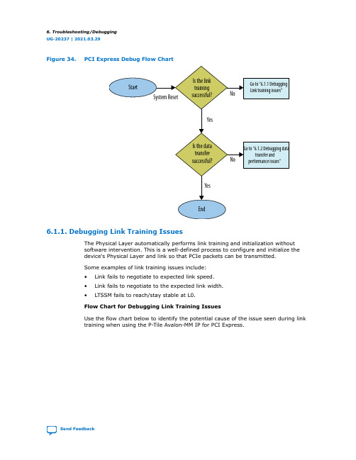
Figure 34.PCI Express Debug Flow Chart6.1.1. Debugging Link Training IssuesThe Physical Layer automatically performs link training and initialization without software intervention. This is a well-defined process to configure and initialize the device's Physical Layer and link so that PCIe packets can be transmitted.Some examples of link training issues include:•Link fails to negotiate to expected link speed.•Link fails to negotiate to the expected link width.•LTSSM fails to reach/stay stable at L0.Flow Chart for Debugging Link Training IssuesUse the flow chart below to identify the potential cause of the issue seen during link training when using the P-Tile Avalon-MM IP for PCI Express.6.Troubleshooting/DebuggingUG-20237 | 2021.03.29Send FeedbackFigure 35.Link Training Debugging FlowNote: (*) Redo the equalization using the Link Equalization Request 8.0 GT/s bit of the Link Status 2 register for 8.0 GT/s or Link Equalization Request 16.0 GT/s bit of the 16.0 GT/s Status Register .Use the following debug tools for debugging link training issues observed on the PCI Express link when using the P-tile Avalon-MM IP for PCI Express.6.Troubleshooting/DebuggingUG-20237 | 2021.03.29Send Feedback6.1.1.1. Generic Tools and UtilitiesYou can use utilities like lspci, setpci to obtain general information of the device like link speed, link width etc.Example: To read the negotiated link speed for the P-Tile device in a system, you can use the following commands:sudo lspci –s $bdf -vvv-s refers to “slot” and is used with the bus/device/function number (bdf) e this command if you know the bdf of the device in the system topology.sudo lspci –d <1172>:$did -vvv-d refers to device and is used with the device ID (vid:did). Use this command to search using the device ID.Figure 36.lspciOutputThe LnkCap under Capabilities indicates the advertised link speed and width capabilities of the device. The LnkSta under Capabilities indicates the negotiated link speed and width of the device.6.1.1.2. SignalTapII Logic AnalyzerUsing the SignalTapII Logic Analyzer , you can monitor the following top-level signals from the P-Tile Avalon-MM IP for PCI Express to confirm the failure symptom for any port type (Root port, Endpoint or TLP Bypass) and configuration (Gen4/Gen3).6.Troubleshooting/DebuggingUG-20237 | 2021.03.29Send Feedback。
FPGA可编程逻辑器件芯片EP1S30F780I6中文规格书

About This Handbook This handbook provides comprehensive information about the Altera®Stratix family of devices.How to Find Information You can find more information in the following ways:■The Adobe Acrobat Find feature, which searches the text of a PDF document. Click the binoculars toolbar icon to open the Find dialog box.■Acrobat bookmarks, which serve as an additional table of contents in PDF documents.■Thumbnail icons, which provide miniature previews of each page, provide a link to the pages.■Numerous links, shown in green text, which allow you to jump to related information.How to Contact Altera For the most up-to-date information about Altera products, go to the Altera world-wide web . For technical support on this product, go to For additional information about Altera products, consult the sources shown below.Information Type USA & Canada All Other Locations T echnical support(800)800-EPLD (3753)(7:00 a.m. to 5:00 p.m. Pacific Time)+1 408-544-87677:00 a.m. to 5:00 p.m. (GMT -8:00) Pacific TimeProduct literature Altera literature servicesNon-technical customer service (800)767-3753+1 408-544-70007:00 a.m. to 5:00 p.m. (GMT -8:00)Pacific TimeFTP siteLogic ElementsTable2–6.M4K RAM Block Configurations (True Dual-Port)Port APort B4K ×12K×21K× 4512 × 8256 × 16512 × 9256 × 184K× 1v v v v v2K× 2v v v v v1K× 4v v v v v512× 8v v v v v256× 16v v v v v512× 9v v 256× 18v vFigure2–17.M4K RAM Block Control SignalsFigure2–18.M4K RAM Block LAB Row InterfaceDigital Signal Processing BlockTable2–16.Multiplier Size & Configurations per DSP blockDSP Block Mode9 × 918 × 1836 × 36 (1)Multiplier Eight multipliers witheight product outputs Four multipliers with fourproduct outputsOne multiplier with oneproduct outputMultiply-accumulator T wo multiply andaccumulate (52 bits)T wo multiply and accumulate (52 bits)–T wo-multipliers adder Four sums of twomultiplier products each T wo sums of twomultiplier products each–Four-multipliers adder T wo sums of fourmultiplier products each One sum of four multiplier products each–。
FPGA可编程逻辑器件芯片EP1S30F1020C5N中文规格书

Error Detection BlockYou can enable the Stratix III device error detection block in the Quartus II software(refer to“Software Support” on page15–11). This block contains the logic necessary tocalculate the 16-bit CRC signature for the configuration CRAM bits in the device.The CRC circuit continues running even if an error occurs. When a soft error occurs,the device sets the CRC_ERROR pin high. Two types of CRC detection check theconfiguration bits:■The CRAM error checking ability (16-bit CRC) during user mode, for use by the CRC_ERROR pin.■For each frame of data, the pre-calculated 16-bit CRC enters the CRC circuitright at the end of the frame data and determines whether or not there is anerror.■If an error occurs, the search engine starts to find the location of the error.■You can shift the error messages out through the JTAG instruction or coreinterface logic while the error detection block continues running.■The JTAG interface reads out the 16-bit CRC result for the first frame and alsoshifts the 16-bit CRC bits to the 16-bit CRC storage registers for test purposes.■You can deliberately introduce single error, double errors, or double errorsadjacent to each other to configuration memory for testing and designverification.1The “Error Detection Registers” section focuses on the first type, the 16-bit CRC only when the device is in user mode.■The 16-bit CRC that is embedded in every configuration data frame.■During configuration, after a frame of data is loaded into the Stratix III device,the pre-computed CRC is shifted into the CRC circuitry.■At the same time, the CRC value for the data frame shifted-in is calculated. Ifthe pre-computed CRC and calculated CRC values do not match, nSTATUS isset low. Every data frame has a 16-bit CRC; therefore, there are many 16-bitCRC values for the whole configuration bitstream. Every device has differentlengths of the configuration data frame.Error Detection RegistersThere is one set of 16-bit registers in the error detection circuitry that stores thecomputed CRC signature. A non-zero value on the syndrome register causes theCRC_ERROR pin to be set high. Figure15–1 shows the block diagram of the errordetection circuitry, syndrome registers, and error injection block.Chapter 16:Programmable Power and Temperature-Sensing Diodes in Stratix III DevicesStratix III External Power Supply Requirementsf For possible values of each power supply, refer to the DC and Switching Characteristicsof Stratix III Devices chapter in volume 2 of the Stratix III Device Handbook.f For detailed guidelines about how to connect and isolate VCCL and VCC power supplypins, refer to the Stratix III Device Family Pin Connections Guidelines.Table16–2.Stratix III Power Supply RequirementsNotes to Table16–2:(1)You can minimize the number of external power sources by driving the left column and supplies with the same voltage regulator. Note thatseparate power planes, decoupling capacitors, and ferrite beads are required for VCCA_PLL and VCCPT when implementing this scheme. (2)V CCPD can be either 2.5 V, 3.0 V, or 3.3 V. For a 3.3-V standard, V CCPD = 3.3 V. For a 3.0-V I/O standard, V CCPD = 3.0V. For 2.5 V and below I/Ostandards, V CCPD = 2.5V.(3)This scheme is for VCCIO = 2.5V.(4)There is one VREF pin per I/O bank. Use an external power supply or a resistor divider network to supply this voltage.Chapter 16:Programmable Power and Temperature-Sensing Diodes in Stratix III DevicesTemperature Sensing DiodeFigure16–1 shows an example of power management for Stratix III devices.Figure16–1.Stratix III Power Management Example (Note1), (2)Notes to Figure16–1:(1)When V CCL = 0.9V, you need a separate voltage regulator.(2)When V CCL = 0.9V, V CCPT and V CC must be ramped before V CCL to minimize V CCL standby current during V CCPT and V CC ramping to full rail.Temperature Sensing DiodeKnowing the junction temperature is crucial for thermal management. A Stratix IIIdevice monitors its die temperature with an embedded temperature sensing diode(TSD). This is done by sensing the voltage level across the TSD. Each temperaturelevel produces a unique voltage across the diode. Use an external analog-to-digitalconverter that measures the voltage difference across the TSD and then converts it to atemperature reading.Chapter 16:Programmable Power and Temperature-Sensing Diodes in Stratix III DevicesConclusionExternal Pin ConnectionsThe Stratix III TSD, located in the top-right corner of the die, requires two pins forvoltage reference. Connect the TEMPDIODEP and TEMPDIODEN pins to the externalanalog-to-digital converter, as shown in Figure16–2.Figure16–2.TEMPDIODEP and TEMPDIODEN External Pin ConnectionsTemperat u reThe TSD is a very sensitive circuit which can be influenced by the noise coupled fromtraces on the board, and possibly within the device package itself, depending ondevice usage. The interfacing device registers temperature based on milivolts ofdifference as seen at the TSD. Switching I/O near the TSD pins can affect thetemperature reading. Altera recommends you take temperature readings duringperiods of no activity in the device (for example, standby mode where no clocks aretoggling in the device), such as when the nearby I/Os are at a DC state and the clocknetworks in the device are disabled.Figure16–3.TSD ConnectionsConclusionAs process geometries get smaller, power and thermal management is becoming morecrucial in FPGA designs. Stratix III devices offer programmable power technologyand selectable core voltage options for low-power operation. Use these features, alongwith speed grade choices, in different permutations to get the best power andperformance combination. Taking advantage of the silicon, the Quartus II software isable to manipulate designs to use the best combination to achieve the lowest power atthe required performance.For thermal management, use the Stratix III temperature sensing diode with anexternal analog-to-digital converter in production devices. This allows you to easilyincorporate this feature in your designs. Being able to monitor the junctiontemperature of the device at any time also allows you to control air flow to the deviceand save power for the whole system.Chapter 16:Programmable Power and Temperature-Sensing Diodes in Stratix III Devices Chapter Revision History。
FPGA可编程逻辑器件芯片EP3CLS100F780I7N中文规格书

Chapter 8:External Memory Interfaces in Stratix III DevicesMemory Interfaces Pin SupportOptional Parity, DM, BWSn, NWSn, ECC and QVLD PinsIn Stratix III devices, you can use any of the DQ pins from the same DQS/DQ groupfor data as parity pins. The Stratix III device family supports parity in ×8/×9,×16/×18, and ×32/×36 modes. There is one parity bit available per eight bits of datapins. Use any of the DQ (or D) pins in the same DQS/DQ group as data for parity asthey are treated, configured, and generated like a DQ pin.DM pins are only required when writing to DDR3, DDR2, DDR SDRAM, andRLDRAM II devices. QDR II+ and QDR II SRAM devices use the BWSn (or NWSn inthe ×8 QDR II SRAM devices) signal to select which byte to write into the memory.Each group of DQS and DQ signals in DDR3, DDR2, and DDR SDRAM devicesrequire a DM pin. There is one DM pin per RLDRAM II device and one BWSn pin per9 bits of data in ×9, ×18, and ×36 QDR II+/QDR II SRAM. The ×8 QDR II SRAMdevice has two BWSn pins per 8 data bits, which are referred to as NWSn pins.A low signal on DM, NWSn, or BWSn indicates that the write is valid. If theDM/BWSn/NWSn signal is high, the memory masks the DQ signals. If the systemdoes not require write data masking, connect the memory DM pins low to indicateevery write data is valid. You can use any of the DQ pins in the same DQS/DQ groupas write data for the DM/BWSn/NWSn signals. Generate the DM or BWSn signalsusing DQ pins and configure the signals similar to the DQ (or D) output signals.Stratix III devices do not support the DM signal in ×4 DDR3 SDRAM or in ×4 DDR2SDRAM interfaces with differential DQS signaling.Some DDR3, DDR2, and DDR SDRAM devices or modules support error correctioncoding (ECC), which is a method of detecting and automatically correcting errors indata transmission. In a 72-bit DDR3, DDR2, or DDR SDRAM interface, typically eightECC pins are used in addition to the 64 data pins. Connect the DDR3, DDR2, andDDR SDRAM ECC pins to a Stratix III device DQS/DQ group. These signals are alsogenerated similar to DQ pins. The memory controller requires encoding and decodinglogic for ECC data. You can also use the extra byte of data for other error checkingmethods.QVLD pins are used in RLDRAM II and QDR II+ SRAM interfaces to indicate readdata availability. There is one QVLD pin per memory device. A high on QVLDindicates that the memory is outputting the data requested. Similar to DQ inputs, thissignal is edge-aligned with the read clock signals (CQ/CQn inQDR II+/QDR II SRAM and QK/QK# in RLDRAM II) and is sent half a clock cyclebefore data starts coming out of the memory. The QVLD pin is not used in theALTMEMPHY megafunction solution for QDR II+ SRAM.For more information about the parity, ECC, and QVLD pins as these pins are treatedas DQ pins refer to “Data and Data-Strobe/Clock Pins” on page8–4.Address and Control/Command PinsAddress and control/command signals are typically sent at a single data rate. Theonly exception is in QDR II SRAM burst-of-two devices, where the read address mustbe captured on the rising edge of the clock while the write address must be capturedon the falling edge of the clock by the memory. There is no special circuitry requiredfor the address and control/command pins. You can use any of the user I/O pins inthe same I/O bank as the data pins.You can also bypass the DQS delay chain to achieve 0° phase shift.Update Enable CircuitryBoth the DQS delay settings and phase-offset settings pass through a register before going into the DQS delay chains. The registers are controlled by the update enable circuitry to allow enough time for any changes in the DQS delay setting bits to arrive at all the delay elements. This allows them to be adjusted at the same time. The update enable circuitry enables the registers to allow enough time for the DQS delay settings to travel from the DQS phase-shift circuitry or core logic to all the DQS logic blocks before the next change. It uses the input reference clock or a user clock from the core to generate the update enable output. The ALTMEMPHY megafunction uses this circuit by default. See Figure 8–14 for an example waveform of the update enable circuitry output.DQS Postamble CircuitryFor external memory interfaces that use a bi-directional read strobe like DDR3, DDR2, and DDR SDRAM, the DQS signal is low before going to or coming from ahigh-impedance state. The state where DQS is low, just after a high-impedance state, is called the preamble. The state where DQS is low, just before it returns to ahigh-impedance state, is called the postamble. There are preamble and postamble specifications for both read and write operations in DDR3, DDR2, and DDR SDRAM. The DQS postamble circuitry ensures that the data is not lost if there is noise on the DQS line during the end of a read operation that occurs while the DQS is in a postamble state.Stratix III devices have a dedicated postamble register that you can control to ground the shifted DQS signal used to clock the DQ input registers at the end of a read operation. This ensures that any glitches on the DQS input signals at the end of the read postamble time do not affect the DQ IOE registers.In addition to the dedicated postamble register, Stratix III devices also have an HDR block inside the postamble enable circuitry. These registers are used if the controller is running at half the frequency of the I/Os.Figure 8–14.Example of a DQS Update Enable WaveformUpdate Ena b le Circuitry OutputSystem ClockDQS Delay Settings (Updated every 8 cycles)DLL Counter Update (Every 8 cycles)6 b itDLL Counter Update (Every 8 cycles)Stratix III External Memory Interface FeaturesChapter Revision HistoryChapter Revision HistoryTable8–13 lists the revision history for this chapter. Table8–13.Chapter Revision History(Part 1 of 2)。
FPGA可编程逻辑器件芯片EP3C40F780I7中文规格书

Chapter 6:Clock Networks and PLLs in Stratix III Devices PLLs in Stratix III DevicesManual Clock SwitchoverIn manual clock switchover mode, the clkswitch signal controls whether inclk0 or inclk1 is selected as the input clock to the PLL. By default, inclk0 is selected. A low-to-high transition on clkswitch and clkswitch being held high for at least three inclk cycles initiates a clock switchover event. You must bring clkswitch back low again in order to perform another switchover event in the future. If you do not require another switchover event in the future, you can leave clkswitch in a logic high state after the initial switch. Pulsing clkswitch high for at least three inclk cycles performs another switchover event. If inclk0 and inclk1 aredifferent frequencies and are always running, the clkswitch minimum high time must be greater than or equal to three of the slower frequency inclk0/inclk1 cycles. Take note that manual switchover is only applicable when both clocks are switching. Figure 6–35 shows the block diagram of the manual switchover circuit.fFor more information about PLL software support in the Quartus II software, refer to the ALTPLL Megafunction User Guide .GuidelinesUse the following guidelines when implementing clock switchover in Stratix III PLLs.■Automatic clock switchover requires that the inclk0 and inclk1 frequencies be within 100% (2×) of each other. Failing to meet this requirement causes the clkbad[0] and clkbad[1] signals to not function properly.■When using manual clock switchover, the difference between inclk0 andinclk1 can be more than 100% (2×). However, differences in frequency and/or phase of the two clock sources will likely cause the PLL to lose lock. Resetting the PLL ensures that the correct phase relationships are maintained between input and output clocks.1Both inclk0 and inclk1 must be running when the clkswitch signal goes high to instantiate the manual clock switchover event. Failing to meet this requirement causes the clock switchover to not function properly.Figure 6–35.Manual Clock Switchover Circuitry in Stratix III PLLsPLLs in Stratix III DevicesTable 6–22 lists the PLL counter selection based on the corresponding PHASECOUNTERSELECT setting.The procedure to perform one dynamic phase-shift step is as follows:1.Set phaseupdown and phasecounterselect as required.2.Assert phasestep for at least two scanclk cycles. Each phasestep pulseenables one phase shift.3.De-assert phasestep.4.Wait for phasedone to go high.5.Repeat steps 1 through 4 as many times as required to perform multiple phase-shifts.All signals are synchronous to scanclk. They are latched on scanclk edges and must meet t su /t h requirements with respect to scanclk edges.Table 6–21.Dynamic Phase-Shifting Control Signals (Part 2 of 2)Table 6–22.Phase Counter Select MappingChapter Revision HistorySection II.I/O InterfacesChapter 7:Stratix III Device I/O FeaturesStratix III I/O Structure Figure7–6.Number of I/Os in Each Bank in EP3SL340 Devices in the 1760-pin FineLine BGA Package (Note1), (2)Notes to Figure7–6:(1)All I/O pin counts include dedicated clock inputs pins. The pin count includes all general purpose I/O, dedicated clock pins, and dual-purposeconfiguration pins. Dedicated configuration pins are not included in the pin count.(2)Figure7–6 is a top view of the silicon die that corresponds to a reverse view for flip chip packages. It is a graphical representation only.Stratix III I/O StructureThe I/O element (IOE) in Stratix III devices contains a bi-directional I/O buffer andI/O registers to support a complete embedded bi-directional single data rate or DDRtransfer. The IOEs are located in I/O blocks around the periphery of the Stratix IIIdevice. There are up to four IOEs per row I/O block and four IOEs per column I/Oblock. The row IOEs drive row, column, or direct link interconnects. The column IOEsdrive column interconnects.The Stratix III bi-directional IOE also supports the following features:■Programmable input delay■Programmable output-current strength■Programmable slew rate■Programmable output delay■Programmable bus-hold■Programmable pull-up resistor■Open-drain output■On-chip series termination with calibration。
- 1、下载文档前请自行甄别文档内容的完整性,平台不提供额外的编辑、内容补充、找答案等附加服务。
- 2、"仅部分预览"的文档,不可在线预览部分如存在完整性等问题,可反馈申请退款(可完整预览的文档不适用该条件!)。
- 3、如文档侵犯您的权益,请联系客服反馈,我们会尽快为您处理(人工客服工作时间:9:00-18:30)。
Manual Clock SwitchoverIn manual clock switchover mode, the clkswitch signal controls whether inclk0 or inclk1 is selected as the input clock to the PLL. By default, inclk0 is selected. A low-to-high transition on clkswitch and clkswitch being held high for at least three inclk cycles initiates a clock switchover event. You must bring clkswitch back low again in order to perform another switchover event in the future. If you do not require another switchover event in the future, you can leave clkswitch in a logic high state after the initial switch. Pulsing clkswitch high for at least three inclk cycles performs another switchover event. If inclk0 and inclk1 aredifferent frequencies and are always running, the clkswitch minimum high time must be greater than or equal to three of the slower frequency inclk0/inclk1 cycles. Take note that manual switchover is only applicable when both clocks are switching. Figure 6–35 shows the block diagram of the manual switchover circuit.fFor more information about PLL software support in the Quartus II software, refer to the ALTPLL Megafunction User Guide .GuidelinesUse the following guidelines when implementing clock switchover in Stratix III PLLs.■Automatic clock switchover requires that the inclk0 and inclk1 frequencies be within 100% (2×) of each other. Failing to meet this requirement causes the clkbad[0] and clkbad[1] signals to not function properly.■When using manual clock switchover, the difference between inclk0 andinclk1 can be more than 100% (2×). However, differences in frequency and/or phase of the two clock sources will likely cause the PLL to lose lock. Resetting the PLL ensures that the correct phase relationships are maintained between input and output clocks.1Both inclk0 and inclk1 must be running when the clkswitch signal goes high to instantiate the manual clock switchover event. Failing to meet this requirement causes the clock switchover to not function properly.Figure 6–35.Manual Clock Switchover Circuitry in Stratix III PLLsChapter 6:Clock Networks and PLLs in Stratix III DevicesPLLs in Stratix III Devices■Applications that require a clock switchover feature and a small frequency drift should use a low-bandwidth PLL. The low-bandwidth PLL reacts more slowly than a high-bandwidth PLL to reference input clock changes. When theswitchover happens, a low-bandwidth PLL propagates the stopping of the clock to the output more slowly than a high-bandwidth PLL. However, be aware that the low-bandwidth PLL also increases lock time.■After a switchover occurs, there may be a finite resynchronization period for the PLL to lock onto a new clock. The exact amount of time it takes for the PLL to re-lock depends on the PLL configuration.■The phase relationship between the input clock to the PLL and the output clock from the PLL is important in your design. Assert areset for at least 10ns after performing a clock switchover. Wait for the locked signal to go high and be stable before re-enabling the output clocks from the PLL.■Figure 6–36 shows how the VCO frequency gradually decreases when the current clock is lost and then increases as the VCO locks on to the backup clock.■Disable the system during clock switchover if it is not tolerant of frequencyvariations during the PLL resynchronization period. You can use the clkbad[0]and clkbad[1] status signals to turn off the PFD (PFDENA = 0) so the VCO maintains its most recent frequency. You can also use the state machine to switch over to the secondary clock. When the PFD is re-enabled, output clock-enable signals (clkena ) can disable clock outputs during the switchover andresynchronization period. Once the lock indication is stable, the system can re-enable the output clocks.Figure 6–36.VCO Switchover Operating FrequencyChapter 6:Clock Networks and PLLs in Stratix III Devices PLLs in Stratix III DevicesChapter 6:Clock Networks and PLLs in Stratix III DevicesPLLs in Stratix III DevicesChapter 6:Clock Networks and PLLs in Stratix III DevicesPLLs in Stratix III DevicesTable6–16.Top/Bottom PLL Reprogramming Bits (Part 2 of 2)Notes to Table6–16:(1)Includes two control bits, rbypass, for bypassing the counter, and rselodd, to select the output clock dutycycle.(2)LSB bit for C9 low-count value is the first bit shifted into the scan chain for Top/Bottom PLLs.(3)LSB bit for C6 low-count value is the first bit shifted into the scan chain for Left/Right PLLs.(4)MSB bit for loop filter is the last bit shifted into the scan chain.Table6–16 lists the scan chain order of PLL components for Top/Bottom PLLs whichhave 10 post-scale counters. The order of bits is the same for the Left/Right PLLs, butthe reconfiguration bits start with the C6 post-scale counter.Figure6–42 shows the scan-chain order of PLL components for the Top/Bottom PLLs. Figure6–42.Scan-Chain Order of PLL Components for Top/Bottom PLLs (Note1)Note to Figure6–42:(1)Left/Right PLLs have the same scan-chain order. The post-scale counters end at C6.Figure6–43 shows the scan-chain bit-order sequence for post-scale counters in allStratix III PLLs.Figure6–43.Scan-Chain Bit-Order Sequence for Post-Scale Counters in Stratix III PLLs。