15-21GHC-YR1S12T;中文规格书,Datasheet资料
17-21SYGC中文资料

元器件交易网EVERLIGHT ELECTRONICS CO.,LTD.Technical Data Sheet 0805 Package Chip LED(1.0mm Height)17-21SYGC/S530-XX/TR8Features․Package in 8mm tape on 7〞diameter reel. ․Compatible with automatic placement equipment. ․Compatible with infrared and vapor phase reflow solder process. ․Mono-color type. ․Pb-free. ․The product itself will remain with in RoHS compliant version.Descriptions․The 17-21 SMD LED is much smaller than lead frame type components, thus enable smaller board size, higher packing density, reduced storage space and finally smaller equipment to be obtained. ․Besides, lightweight makes them ideal for miniature applications. etc.Applications․Backlighting in dashboard and switch. ․Telecommunication: indicator and backlighting in telephone and fax. ․Flat backlight for LCD, switch and symbol. ․General use.Device Selection GuidePart No. 17-21SYGC/S530-XX/TR8 Chip Material AlGaInP Emitted Color Brilliant Yellow Green Resin Color Water ClearEverlight Electronics Co., Ltd. Device No. : DSE-171-103 Prepared date:27-Oct-2007Rev. 2Page: 1 of 9Prepared by:Zhouhua元器件交易网EVERLIGHT ELECTRONICS CO.,LTD.17-21SYGC/S530-XX/TR8Package Outline Dimensions-+Note: The tolerances unless mentioned is ±0.1mm, Unit = mmEverlight Electronics Co., Ltd. Device No. : DSE-171-1031.05 Prepared date:27-Oct-2007Rev. 2Page: 2 of 9Prepared by:Zhouhua元器件交易网EVERLIGHT ELECTRONICS CO.,LTD.17-21SYGC/S530-XX/TR8Absolute Maximum Ratings (Ta=25℃)Parameter Reverse Voltage Forward Current Peak Forward Current (Duty 1/10 @1KHz) Power Dissipation ElectrostaticDischarge (HBM) Operating Temperature Storage Temperature Soldering Temperature Symbol VR IF IFP Pd ESD Topr Tstg Tsol Rating 5 25 60 60 2000 -40 ~ +85 -40~ +90 Reflow Soldering:260 ℃ for 10 sec Hand Soldering:350℃ for 3 sec Unit V mA mA mW V ℃ ℃Electro-Optical Characteristics (Ta=25℃)Parameter Symbol *Chip Rank Min. Typ. Max. Unit ConditionLuminous IntensityIvE1 E2 E3 E4 -------------------------12 17 22 27 -------------------------17 23 31 41 140 575 573 20 2.0 -------------------------------------2.4 10mcdViewing Angle Peak WavelengthDominant Wavelength2θ1/2 λp λd △λ VF IRdeg nm nm nm V μAIF=20 mASpectrum Radiation Bandwidth Forward VoltageReverse CurrentVR=5VEverlight Electronics Co., Ltd. Device No. : DSE-171-103 Prepared date:27-Oct-2007Rev. 2Page: 3 of 9Prepared by:Zhouhua元器件交易网EVERLIGHT ELECTRONICS CO.,LTD.17-21SYGC/S530-XX/TR8Typical Electro-Optical Characteristics CurvesEverlight Electronics Co., Ltd. Device No. : DSE-171-103 Prepared date:27-Oct-2007Rev. 2Page: 4 of 9Prepared by:Zhouhua元器件交易网EVERLIGHT ELECTRONICS CO.,LTD.17-21SYGC/S530-XX/TR8Label explanationCAT: Luminous Intensity Rank HUE: Dom. Wavelength Rank REF: Forward Voltage RankReel DimensionsNote: The tolerances unless mentioned is ±0.1mm, Unit = mmEverlight Electronics Co., Ltd. Device No. : DSE-171-103 Prepared date:27-Oct-2007Rev. 2Page: 5 of 9Prepared by:Zhouhua元器件交易网EVERLIGHT ELECTRONICS CO.,LTD.17-21SYGC/S530-XX/TR8Carrier Tape Dimensions: Loaded quantity 3000 PCS per reelNote: The tolerances unless mentioned is ±0.1mm , Unit = mmMoisture Resistant PackagingLabelAluminum moisture-proof bagDesiccantLabelEverlight Electronics Co., Ltd. Device No. : DSE-171-103 Prepared date:27-Oct-2007Rev. 2Page: 6 of 9Prepared by:Zhouhua元器件交易网EVERLIGHT ELECTRONICS CO.,LTD.17-21SYGC/S530-XX/TR8Reliability Test Items And ConditionsThe reliability of products shall be satisfied with items listed below. Confidence level:90% LTPD:10%No. 1Items Reflow SolderingTest Condition Temp. : 260℃±5℃ Min. 5sec. H : +100℃ 15min ∫ 5 min L : -40℃ 15min H : +100℃ 5min ∫ 10 sec L : -10℃ 5min Temp. : 100℃ Temp. : -40℃ IF = 20 mA 85℃/ 85%RHTest Sample Hours/Cycles Size 6 Min. 300 Cycles 22 PCS.Ac/Re 0/12Temperature Cycle22 PCS.0/13Thermal Shock High Temperature Storage Low Temperature Storage DC Operating Life High Temperature / High Humidity300 Cycles 1000 Hrs. 1000 Hrs. 1000 Hrs. 1000 Hrs.22 PCS.0/14 5 6 722 PCS. 22 PCS. 22 PCS. 22 PCS.0/1 0/1 0/1 0/1Everlight Electronics Co., Ltd. Device No. : DSE-171-103 Prepared date:27-Oct-2007Rev. 2Page: 7 of 9Prepared by:Zhouhua元器件交易网EVERLIGHT ELECTRONICS CO.,LTD.17-21SYGC/S530-XX/TR8Precautions For Use 1. Over-current-proof Customer must apply resistors for protection, otherwise slight voltage shift will cause big current change ( Burn out will happen ). 2. Storage 2.1 Do not open moisture proof bag before the products are ready to use.2.2 Before opening the package: The LEDs should be kept at 30℃ or less and 90%RH or less. 2.3 After opening the package : The LEDs should be kept at 30℃ or less and 70%RH or less(Floor life). However, it's recommended that the LEDs should be used within 168 hours (7 days) after opening the package. If unused LEDs remain, it should be stored in moisture proof packages. 2.4 If the moisture absorbent material (silica gel) has faded away or the LEDs have exceeded the storage time, baking treatment should be performed using the following conditions. Baking treatment : 60±5℃ for 24 hours. 3. Soldering Condition 3.1 Pb-free solder temperature profile3.2 Reflow soldering should not be done more than two times. 3.3 When soldering, do not put stress on the LEDs during heating. 3.4 After soldering, do not warp the circuit board.Everlight Electronics Co., Ltd. Device No. : DSE-171-103 Prepared date:27-Oct-2007Rev. 2Page: 8 of 9Prepared by:Zhouhua元器件交易网EVERLIGHT ELECTRONICS CO.,LTD.17-21SYGC/S530-XX/TR84.Soldering Iron Each terminal is to go to the tip of soldering iron temperature less than 350℃ for 3 seconds within once in less than the soldering iron capacity 25W. Leave two seconds and more intervals, and do soldering of each terminal. Be careful because the damage of the product is often started at the time of the hand solder. 5.Repairing Repair should not be done after the LEDs have been soldered. When repairing is unavoidable, a double-head soldering iron should be used (as below figure). It should be confirmed beforehand whether the characteristics of the LEDs will or will not be damaged by repairing.EVERLIGHT ELECTRONICS CO., LTD. Office: No 25, Lane 76, Sec 3, Chung Yang Rd, Tucheng, Taipei 236, Taiwan, R.O.CTel: 886-2-2267-2000, 2267-9936 Fax: 886-2267-6244, 2267-6189, 2267-6306 Everlight Electronics Co., Ltd. Device No. : DSE-171-103 Prepared date:27-Oct-2007Rev. 2Page: 9 of 9Prepared by:Zhouhua。
IHW15N120R2H15R1202pdf
min.
-
Value typ.
342 90 1.3 1.3
Unit max.
-
2) Leakage inductance L σ a nd Stray capacity C σ due to dynamic test circuit in Figure E.
Power Semiconductors
3
-
Reverse transfer capacitance
Crss
f=1MHz
-
Gate charge
QGate
VCC=960V, IC=15A
-
VGE=15V
Internal emitter inductance
LE
-
measured 5mm (0.197 in.) from case
1530 49 39 133
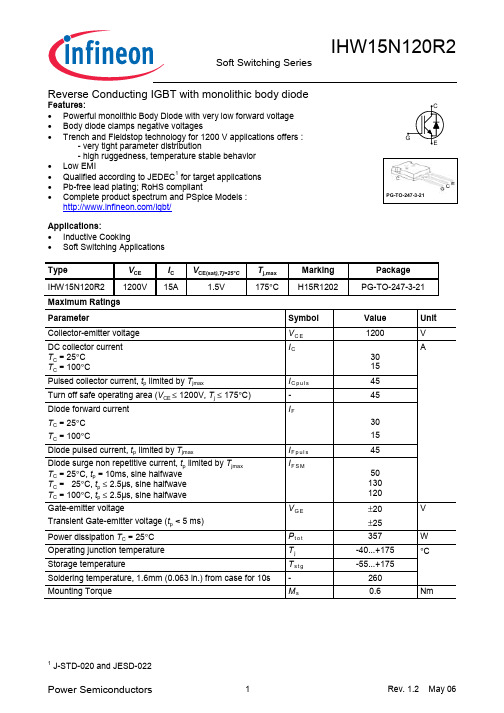
IHW15N120R2
Soft Switching Series
Reverse Conducting IGBT with monolithic body diode
Features: • Powerful monolithic Body Diode with very low forward voltage • Body diode clamps negative voltages • Trench and Fieldstop technology for 1200 V applications offers :
13
- pF - nC
- nH
Switching Characteristic, Inductive Load, at Tj=25 °C
Parameter
Symbol
电气设备产品说明书:Eaton V12-T21

V12-T21-121Power Factor Correction CapacitorsLow Voltage Fixed and AutomaticPower Factor Correction Systems21Power Factor Correction CapacitorsProduct Description. . . . . . . . . . . . . . . . . . . . . . . . . . . . . . . . . . . . . . . V12-T21-2Product History . . . . . . . . . . . . . . . . . . . . . . . . . . . . . . . . . . . . . . . . . . V12-T21-2Product History Time Line. . . . . . . . . . . . . . . . . . . . . . . . . . . . . . . . . . V12-T21-2Replacement Capabilities . . . . . . . . . . . . . . . . . . . . . . . . . . . . . . . . . . V12-T21-3Technology Upgrades . . . . . . . . . . . . . . . . . . . . . . . . . . . . . . . . . . . . . V12-T21-4Further Information . . . . . . . . . . . . . . . . . . . . . . . . . . . . . . . . . . . . . . . V12-T21-5Pricing Information . . . . . . . . . . . . . . . . . . . . . . . . . . . . . . . . . . . . . . .V12-T21-52121Power Factor Correction CapacitorsPower FactorCorrection CapacitorsUNIPAK and AUTOVARProduct DescriptionPower factor correctioncapacitors and harmonicfilters are an essential partof modern electric powersystems. Power factorcorrection capacitors arethe simplest and mosteconomical means ofincreasing the transmissioncapacity of a power system,minimizing energy losses andcorrecting load power factor.In addition, power factorpenalties can be reducedand power quality can begreatly enhanced.There are two main reasonsto correct poor power factor.The first is to reduce oreliminate a power factorpenalty charged by your localutility. Another reason is thatyour existing transformeris, or shortly will be, at fullcapacity and installing powerfactor correction capacitorscan be a very cost-effectivesolution to installing a brandnew service.Depending on the amountof power factor correction(amount of kVAR requiredfor the electrical system toimprove the power factor)and the dynamic nature of theload, a fixed or switchedcapacitor bank may be thebest solution. When capacitybecomes a problem, thechoice of a solution will bedependent upon the size ofthe increase needed. Likeall power quality solutions,there are many factors thatneed to be considered whendetermining which solutionwill be best to solve yourpower factor problem.Harmonic FilteringAs the world becomes moredependent on electric andelectronic equipment, thelikelihood that the negativeimpact of harmonic distortionincreases dramatically. Theefficiency and productivitygains from these increasinglysophisticated pieces ofequipment have a negativeside effect—increasedharmonic distortion in thepower lines. The difficultthing about harmonicdistortion is determining thecause. Once this has beendetermined, the solution canbe easy. Passive harmonicfiltering equipment willmitigate specific harmonicissues, and correct poorpower factor as well.Product HistoryEaton’s Cutler-Hammer®power factor correctionproduct line began as SpragueElectric in Massachusetts in1942. They were the firstmanufacturers of drycapacitor cells in the UnitedStates. Throughout the next40 years, they manufacturedcapacitors in both the dry andoil-filled designs.In 1986, the company waspurchased and renamedCommonwealth Sprague.Eaton’s Cutler-HammerPower Quality Division begana name brand relationshipwith Commonwealth Spraguein 2001, and purchased theCommonwealth Spraguecapacitor systems businessin 2003. At that time,manufacturing was movedto the Asheville, NC,manufacturing plant.Product History Time LineV12-T21-2V12-T21-32121Power Factor Correction CapacitorsReplacement CapabilitiesCapacitor Cells—Dry-Type ●T erminals: Threaded for secure connection, all sizes. 10 kVAC stand-off terminal bushings. Rated for 30 kV BIL ●Dielectric fill: Thermosetting polymer resin ●Flash point: +415°F (+212°C)●Fire point: +500°F (+260°C)●Dielectric film:Self-healing metallized polypropylene. Losses less than 1/2 watt per kVAR ●Pressure-sensitiveinterrupter: Built-in, three-phase interrupter design. UL ® Recognized. Removes capacitor from line before internal pressures can cause case rupture ●Discharge resistors:Reduce residual voltage to less than 50V within one minute of deenergization. Mounted on terminal stud assemblies. Selected for 20-year nominal life. Exceeds NEC ® requirements●Capacitor operating temperature: –40°F (–40°C) to +115°F (+46°C)PCDM Cell Showing Threaded Nut and Stud T erminal ConnectionDry Cell ChartNotes1kVAR rating standard. NEMA ® kVAR tolerance is +15%–0%.2Catalog number as shown is for three-phase units.Dry-type. Thermoplastic encapsulationmedium. On all units, customer must provide overcurrent protection as tabulated or equivalent (fuse interruption rating shall be100,000A or greater). All units supplied unpainted. Case material terne plate steel approximately 0.017 thick.Voltage Rating kVAR 1Height—Inches (mm)Approximate Weight—Lbs (kg)Catalog Number 22400.50 4.00 (101.6) 2.1 (1.0)243PCDMF 240 1.00 4.00 (101.6) 2.1 (1.0)443PCDMF 240 1.50 4.00 (101.6) 2.1 (1.0)643PCDMF 240 2.00 4.00 (101.6) 2.1 (1.0)843PCDMF 240 2.50 4.50 (114.3) 2.6 (1.2)1043PCDMF 240 3.00 5.50 (139.7) 3.2 (1.5)12X43PCDMF 240 4.00 6.00 (152.4) 3.5 (1.6)16S43PCDMF 240 5.00 5.00 (127.0) 2.6 (1.2)523PCDMF 240 6.25 6.00 (152.4) 3.2 (1.5)6A23PCDMF 2407.50 6.00 (152.4) 3.5 (1.6)7X23PCDMF 2408.337.00 (177.8) 3.5 (1.6)8B23PCDMF 480 1.00 4.00 (101.6) 2.1 (1.0)143PCDMF 480 2.00 4.00 (101.6) 2.1 (1.0)243PCDMF 480 2.50 4.00 (101.6) 2.1 (1.0)2X43PCDMF 480 3.00 4.00 (101.6) 2.1 (1.0)343PCDMF 480 4.00 4.00 (101.6) 2.1 (1.0)443PCDMF 480 5.00 4.00 (101.6) 2.1 (1.0)543PCDMF 480 6.00 4.00 (101.6) 2.1 (1.0)643PCDMF 4807.50 4.00 (101.6) 2.1 (1.0)7X43PCDMF 4808.00 4.00 (101.6) 2.1 (1.0)843PCDMF 48010.00 5.00 (127.0) 2.6 (1.2)1043PCDMF 48012.50 5.50 (139.7) 3.2 (1.5)12X43PCDMF 48015.00 6.00 (152.4) 3.2 (1.5)1543PCDMF 48016.67 6.00 (152.4) 3.5 (1.6)16S43PCDMF 48017.507.00 (177.8) 3.5 (1.6)17X43PCDMF 48020.007.00 (177.8) 4.2 (1.9)2043PCDMF 600 2.00 4.00 (101.6) 2.1 (1.0)263PCDMF 600 2.50 4.00 (101.6) 2.1 (1.0)2X63PCDMF 600 5.00 4.00 (101.6) 2.1 (1.0)563PCDMF 6007.50 4.00 (101.6) 2.1 (1.0)7X63PCDMF 60010.00 5.00 (127.0) 2.6 (1.2)1063PCDMF 60012.50 6.00 (152.4) 3.2 (1.5)12X63PCDMF 60015.00 6.00 (152.4) 3.5 (1.6)1563PCDMF 60016.677.00 (177.8) 3.5 (1.6)16S63PCDMF 60017.507.00 (177.8) 3.5 (1.6)17X63PCDMF 60020.008.75 (222.3)5.0 (2.3)2063PCDMF2121Power Factor Correction CapacitorsTechnology UpgradesUNIPAKUNIPAKFixed power factor correctionfor retrofit and upgrades.Units are available in 240–600V and 1–400 kVAR ratingsfor retail, commercial andindustrial applications forsingle point correction. Unitscan also be configured toinclude harmonic filters inorder to reduce harmonicsin applications with largeamounts of nonlinear loads,such as variable speed drives.They are most commonlyapplied to low voltagemotors, motor controlcenters and incomingswitchboards.UNIPUMPUNIPUMPFixed power factor correctionfor retrofit or upgrade ofindoor or outdoor pumpmotor applications. Unitsare available in 240–600Vand 2–20 kVAR ratings. Unitsinclude mounting bracketsand a 4-foot flexible powercable attached for simplemounting and connection.AUTOVARAUTOVAR 300AUTOVAR 600Switched power factorcorrection for retrofit orupgrade at the substationof facility level. An intelligentcontroller senses thecustomer’s current powerfactor, and automaticallysteps on and off stagesof capacitance in order toachieve the customer’sprogrammed target powerfactor. Units are available in240–600V and 25–840 kVARratings in wall and floor-mountdesigns. Higher ratings areavailable—contact the factoryfor assistance. Units canalso be configured to includeharmonic filters in orderto reduce harmonics inapplications with largeamounts of nonlinear loads,such as variable speed drives.Harmonic Correction UnitHarmonic Correction UnitsActive harmonic filtersprovide active harmoniccontrol. The active harmonicfilter will monitor the distortedelectrical signal, determinethe frequency and magnitudeof the harmonic content, andthen cancel those harmonicswith the dynamic injectionof opposing current. Activeharmonic control providesthe benefit of traditionalpassive filters with simplerengineering requirements,easier and less expensiveinstallation, comprehensivecontrol, and assuredcompliance with the IEEE®519-1992 standard.Medium Voltage UNIVARand AUTOVARMetal-Enclosed Medium VoltagePower Factor Correction SystemUNIVAR Fixed Medium Voltage PFC UnitEaton’s Cutler-Hammer metal-enclosed medium voltagecapacitors, systems andharmonic filters are designedfor indoor or outdoorcommercial, industrial andutility power systemsrequiring motor start support,power factor correction,harmonic filtering, IEEE 519compliance and increasedsystem capacity. Fixed motorstart capacitors are availableto assist in motor startingapplications. Engineereddesigns are available witha host of options andaccessories to fit therequirements and the desiredconfigurations of virtually anyinstallation. Single-stage andmulti-stage, tuned or de-tunedfilter banks can be supplied.Metal-enclosed mediumvoltage capacitor banksare designed for industrial,commercial and utilitypower systems involvingmotors, feeder circuits, andtransmission and distributionlines where power factorimprovement is required.V12-T21-4V12-T21-52121Power Factor Correction CapacitorsFurther InformationPricing InformationPrice and Availability Digest (PAD)Vista/VISTALINE™ Discount Symbol C10-S27 for SystemsVista/VISTALINE Discount Symbol C10-ST for Replacement Capacitor Cells Price List—PL02607002EPublication Number DescriptionTD02607001E Low voltage power factor correction capacitor banks and harmonic filtersTD02607011EMetal-enclosed medium voltage power factor correction and harmonic filter systems。
PMS150C datasheet V001_CN-1
PMS150C系列8位IO类型单片机数据手册第0.01版2016年3月17日Copyright 2016 by PADAUK Technology Co., Ltd., all rights reserved重要声明应广科技保留权利在任何时候变更或终止产品,建议客户在使用或下单前与应广科技或代理商联系以取得最新、最正确的产品信息。
应广科技不担保本产品适用于保障生命安全或紧急安全的应用,应广科技不为此类应用产品承担任何责任。
关键应用产品包括,但不仅限于,可能涉及的潜在风险的死亡,人身伤害,火灾或严重财产损失。
应广科技不承担任何责任来自于因客户的产品设计所造成的任何损失。
在应广科技所保障的规格范围内,客户应设计和验证他们的产品。
为了尽量减少风险,客户设计产品时,应保留适当的产品工作范围安全保障。
PMS150C不适用于交流供电阻容降压或者电源纹波大,EFT要求高的应用,请注意不要将PMS150C用于这种特殊要求的产品中。
提供本文档的中文简体版是为了便于了解,请勿忽视文中英文的部份,因为其中提供有关产品性能以及产品使用的有用信息,应广科技暨代理商对于文中可能存在的差错不承担任何责任,建议参考本档英文版。
目录1. 单片机特点 (7)1.1. 系统功能 (7)1.2. CPU特点 (7)2. 系统概述和方框图 (8)3. 引脚功能说明 (9)4. 器件电气特性 (10)4.1 直流交流电气特性 (10)4.2 工作范围 (11)4.3 IHRC频率与VDD关系曲线图 (12)4.4 ILRC频率与VDD关系曲线图 (12)4.5 IHRC频率与温度关系曲线图(校准到16MHz) (13)4.6 ILRC频率与温度关系曲线图 (13)4.7 工作电流与VDD、系统时钟CLK=IHRC/n曲线图 (14)4.8 工作电流与VDD、系统时钟CLK=ILRC/n曲线图 (14)4.9 引脚上拉电阻曲线图 (15)4.10 引脚输出驱电流(Ioh)与灌电流(Iol) 曲线图 (15)4.11 引脚输出输入高电压与低电压(V IH / V IL) 曲线图 (16)5. 功能概述 (17)5.1程序内存——OTP (17)5.2 开机流程 (17)5.3 数据存储器 – SRAM (18)5.4 振荡器和时钟 (18)5.4.1内部高频振荡器和内部低频振荡 (18)5.4.2芯片校准 (18)5.4.3 IHRC频率校准与系统时钟 (19)5.4.4系统时钟和LVR基准位 (20)5.5 16位定时器 (Timer16) (21)5.6 看门狗定时器 (22)5.7 中断 (22)5.8 省电与掉电 (24)5.8.1省电模式(stopexe) (24)5.8.2掉电模式(stopsys) (25)5.8.3 唤醒 (26)5.9 IO引脚 (27)5.10 复位和LVR (28)5.10.1复位 (28)6. IO 寄存器 (29)6.1 标志寄存器(flag),IO 地址 =0x00 (29)6.2 堆栈指针寄存器(sp),IO地址 =0x02 (29)6.3 时钟控制寄存器(clkmd),IO地址 =0x03 (29)6.4 中断允许寄存器(inten),IO地址 =0x04 (30)6.6 Timer16控制寄存器(t16m),IO地址 =0x06 (30)6.7 外部晶体振荡器控制寄存器(eoscr,只写),IO地址 =0x0a (31)6.8 中断缘选择寄存器 (integs), IO地址 =0x0c (31)6.9 端口A数字输入启用寄存器(padier), IO 地址 =0x0d (31)6.10 端口A数据寄存器(pa),IO地址 =0x10 (31)6.11 端口A控制寄存器(pac),IO地址 =0x11 (31)6.12 端口A上拉控制寄存器(paph),IO地址 =0x12 (31)6.13 杂项寄存器(misc), IO 地址 =0x3b (32)7. 指令 (33)7.1 数据传输类指令 (34)7.2 算术运算类指令 (36)7.3 移位元元运算类指令 (38)7.4 逻辑运算类指令 (39)7.5 位运算类指令 (41)7.6 条件运算类指令 (41)7.7 系统控制类指令 (42)7.8 指令执行周期综述 (44)7.9 指令影响标志的综述 (45)8. 特别注意事项 (46)8.1. 使用IC时 (46)8.1.1. IO使用与设定 (46)8.1.2. 中断 (46)8.1.3. 切换系统时钟 (47)8.1.4. 掉电模式、唤醒以及看门狗 (47)8.1.5. TIMER16溢出时间 (47) (47)8.1.6. LVR8.1.7. 指令 (47)8.1.8. RAM定义限制 (47)8.1.9. 烧录方法 (48)8.2. 使用ICE时 (48)修订历史:修订日期描述初版0.01 2016/3/17PMS150B 和PMS150C 主要差异表PMS150B 与PMS150C 主要差异列举如下:项目 功能PMS150BPMS150C1 ILRC 频率 110KHz@5.0V ,25oC 62KHz@5.0V ,25o C (VDD 变化对ILRC 有影响) 2 LVR 2.8V,2.2V,2.0V 4.0V,3.5V,3.0V,2.75V 2.5V,2.2V,2.0V,1.8V 3 RAM 60 bytes64 bytes 4 PA5口输入模式上拉电阻 没有有5 工作温度0o C ~70o C -20o C ~70o C6省电模式功耗(stopexe ) 40uA@3.3V3 uA@3.3V7 IO 输出电流 17mA/-7mA@5.0V普通模式:14.5mA/-10.5mA@5.0V低驱动模式:5mA/-3.5mA@5.0V 8 看门狗定时器溢时 4096,16384,65536 ILRC 时钟周期8192,16384,65536,262144 ILRC 时钟周期9 唤醒时间 快速模式:1024 T IHRC 普通模式:1024 T ILRC 快速模式:32 T ILRC 普通模式:2048 T ILRC 10 开机时间快速模式:2048 T IHRC 普通模式:1024 T ILRC快速模式:32 T ILRC 普通模式:2048 T ILRC 11系统保留OTP 区 0x3F8~0x3FF(8 word) 0x3F0~0x3FF(16 word)12 ILRC 做系统时钟源 ILRC,ILRC/4 ILRC,ILRC/4,ILRC/16 13支持ICE 类型PDK3S-I-001/002/003, 5S-I-S015S-I-S011. 单片机特点1.1. 系统功能◆时钟模式:内部高频振荡器、内部低频振荡器◆硬件16位定时器◆快速唤醒功能◆ 6 个带输入上拉电阻IO引脚,且做输出时具有可选的电流驱动能力◆1个外部中断输入引脚◆每个引脚都可弹性设定唤醒功能◆8级LVR可选◆工作频率0 ~ 8MHz@VDD≧3V; 0 ~ 4MHz@VDD≧2.2V; 0 ~ 2MHz@VDD≧2.0V;◆工作电压:2.0V ~ 5.5V◆工作温度:-20 o C ~70 o C◆功耗特性:I operating ~ 0.3mA@1MIPS, VDD=3.3VI operating ~ 13uA@ILRC=62KHz, VDD=3.3VI powerdown ~ 0.5uA@VDD=3.3V1.2. CPU特点◆工作模式:单一处理单元的工作模式◆ 1KW OTP程序内存◆ 64字节数据存储器◆提供79条指令◆绝大部分指令都是单周期(1T)指令◆可程序设定的堆栈深度◆所有的数据存储器都可当数据指针(index pointer)◆独立的IO地址以及存储地址方便程序开发2. 系统概述和方框图PMS150C是一个IO类型、完全静态,以OTP为程序存储基础的单片机。
STPSC15H12G2Y-TR 15A 1200V SiC 双极性对流电阻芯片说明书

STPSC15H12G2Y-TRNCD²PAK HVKFeatures•AEC-Q101 qualified•No or negligible reverse recovery•Switching behavior independent of temperature •Robust high voltage periphery •PPAP capable•Operating T j from -40 °C to 175 °C•D²PAK HV creepage distance (anode to cathode) = 5.38 mm min.•ECOPACK2 compliantApplications•OBC •DC/DC •PFCDescriptionThis 15 A, 1200 V SiC diode is an ultra-high performance power Schottky diode. It is manufactured using a silicon carbide substrate. The wide band gap material allows the design of a Schottky diode structure with a 1200 V rating. Due to the Schottky construction, no recovery is shown at turn-off and ringing patterns are negligible. The minimal capacitive turn-off behavior is independent of temperature.Housed in D 2PAK HV, this diode is perfectly suited for a usage in PFC applications,in OBC, DC/DC for EV, easing the compliance to IEC-60664-1.The STPSC15H12G2Y-TR will boost performances in hard switching conditions. Its high forward surge capability ensures good robustness during transient phases.Automotive 1200 V, 15 A, silicon carbide power Schottky diodeSTPSC15H12G2Y-TRDatasheetSTPSC15H12G2Y-TRCharacteristics 1CharacteristicsTable 1. Absolute ratings (limiting values at 25 °C, unless otherwise specified)1.(dP tot/dT j) < (1/R th(j-a)) condition to avoid thermal runaway for a diode on its own heatsink.Table 2. Thermal resistance parametersTable 3. Static electrical characteristics1.Pulse test: t p = 5 ms, δ < 2%2.Pulse test: t p = 500 µs, δ < 2%To evaluate the conduction losses, use the following equation:•P = 1.09 x I F(AV) + 0.0775 x I F2(RMS)For more information, please refer to the following application notes related to the power losses:•AN604: Calculation of conduction losses in a power rectifier•AN4021: Calculation of reverse losses on a power diodeSTPSC15H12G2Y-TRCharacteristicsTable 4. Dynamic electrical characteristics1.Most accurate value for the capacitive charge: Q cj V R= ∫0V R C j V dVSTPSC15H12G2Y-TRCharacteristics (curves) 1.1Characteristics (curves)STPSC15H12G2Y-TR Characteristics (curves)2Package informationIn order to meet environmental requirements, ST offers these devices in different grades of ECOPACK packages,depending on their level of environmental compliance. ECOPACK specifications, grade definitions and product status are available at: . ECOPACK is an ST trademark.2.1D²PAK high voltage package information•Epoxy meets UL94, V0Figure 9.D²PAK high voltage package outlineSTPSC15H12G2Y-TRPackage informationSTPSC15H12G2Y-TRD²PAK high voltage package information Table 5. D²PAK high voltage package mechanical dataFigure 10. D²PAK high voltage footprint in mm2.1.1Creepage distance between Anode and CathodeTable 6. Creepage distance between anode and cathodeNote:D²PAK HV creepage distance (anode to cathode) = 5.38 mm min. (refer to IEC 60664-1)Figure 11. Creepage with top coatingFigure 12. Creepage without top coatingSTPSC15H12G2Y-TRD²PAK high voltage package informationSTPSC15H12G2Y-TROrdering information 3Ordering informationTable 7. Ordering informationRevision historyTable 8. Document revision historyIMPORTANT NOTICE – PLEASE READ CAREFULLYSTMicroelectronics NV and its subsidiaries (“ST”) reserve the right to make changes, corrections, enhancements, modifications, and improvements to ST products and/or to this document at any time without notice. Purchasers should obtain the latest relevant information on ST products before placing orders. ST products are sold pursuant to ST’s terms and conditions of sale in place at the time of order acknowledgement.Purchasers are solely responsible for the choice, selection, and use of ST products and ST assumes no liability for application assistance or the design of Purchasers’ products.No license, express or implied, to any intellectual property right is granted by ST herein.Resale of ST products with provisions different from the information set forth herein shall void any warranty granted by ST for such product.ST and the ST logo are trademarks of ST. For additional information about ST trademarks, please refer to /trademarks. All other product or service names are the property of their respective owners.Information in this document supersedes and replaces information previously supplied in any prior versions of this document.© 2020 STMicroelectronics – All rights reservedSTPSC15H12G2Y-TR。
Ra-01S规格书说明书
Ra-01S规格书版本V1.1版权©2020免责申明和版权公告本文中的信息,包括供参考的URL地址,如有变更,恕不另行通知。
文档“按现状”提供,不负任何担保责任,包括对适销性、适用于特定用途或非侵权性的任何担保,和任何提案、规格或样品在他处提到的任何担保。
本文档不负任何责任,包括使用本文档内信息产生的侵犯任何专利权行为的责任。
本文档在此未以禁止反言或其他方式授予任何知识产权使用许可,不管是明示许可还是暗示许可。
文中所得测试数据均为安信可实验室测试所得,实际结果可能略有差异。
文中提到的所有商标名称、商标和注册商标均属其各自所有者的财产,特此声明。
最终解释权归深圳市安信可科技有限公司所有。
注意由于产品版本升级或其他原因,本手册内容有可能变更。
深圳市安信可科技有限公司保留在没有任何通知或者提示的情况下对本手册的内容进行修改的权利。
本手册仅作为使用指导,深圳市安信可科技有限公司尽全力在本手册中提供准确的信息,但是深圳市安信可科技有限公司并不确保手册内容完全没有错误,本手册中的所有陈述、信息和建议也不构成任何明示或暗示的担保。
文件制定/修订/废止履历表版本日期制定/修订内容制定核准V1.02020.8.12首版徐V1.12020.8.19更新部分参数徐目录一、产品概述 (5)二、电气参数 (6)三、外观尺寸 (8)四、管脚定义 (10)五、原理图 (11)六、设计指导 (12)七、回流焊曲线图 (14)八、包装信息 (15)九、联系我们 (15)一、产品概述安信可LoRa系列模块(Ra-01S)由安信可科技设计开发。
该模组用于超长距离扩频通信,其射频芯片SX1268主要采用LoRa™远程调制解调器,用于超长距离扩频通信,抗干扰性强,能够最大限度降低电流消耗。
借助SEMTECH的LoRa™专利调制技术,SX1268具有超过-148dBm的高灵敏度,+22dBm的功率输出,传输距离远,可靠性高。
同时,相对传统调制技术,LoRa™调制技术在抗阻塞和选择方面也具有明显优势,解决了传统设计方案无法同时兼顾距离、抗干扰和功耗的问题。
19-213GHC-YR1S23T;中文规格书,Datasheet资料

Technical Data Sheet0603 Package Chip LED (0.6 mm Height)19-213/GHC-YR1S2/3T Features․Package in 8mm tape on 7〞diameter reel.․Compatible with automatic placement equipment.․Compatible with infrared and vapor phase reflowsolder process.․Mono-color type.․Pb-free.Descriptions․The 19-213 SMD Taping is much smaller thanlead frame type components, thus enable smallerboard size, higher packing density, reducedstorage space and finally smaller equipment to beobtained.․Besides, lightweight makes them ideal forminiature applications. etc.Applications․Automotive: backlighting in dashboard and switch.․Telecommunication: indicator and backlighting intelephone and fax.․Flat backlight for LCD, switch and symbol.․General use.Device Selection GuideChipLens Color Part No.ColorMaterial Emitted19-213/GHC-YR1S2/3T InGaN Brilliant Green Water Clear19-213/GHC-YR1S2/3TNote: The tolerances unless mentioned is ±0.1mm ,Unit = mm19-213/GHC-YR1S2/3T Absolute Maximum Ratings (Ta=25℃)Parameter SymbolRatingUnitReverse Voltage V R 5 VForward Current I F 25 mAOperating Temperature Topr -40 ~ +85 ℃Storage Temperature Tstg -40 ~ +90 ℃Soldering Temperature Tsol260(for 5 second)℃Electrostatic Discharge ESD 150 VPower Dissipation Pd 110 mWPeak Forward Current(Duty 1/10 @1KHz)I FP 100 mAElectro-Optical Characteristics (Ta=25℃)Parameter Symbol Min. Typ. Max. Unit Condition Luminous Intensity Iv 112 ---- 285 mcdViewing Angle2θ1/2 ----- 120 ----- degPeak Wavelengthλp ----- 518 ----- nmDominant Wavelengthλd520 ----- 535 nmSpectrum RadiationBandwidth△λ----- 35 ----- nm Forward Voltage V F----- 3.5 4.0 VI F=20mAReverse Current I R ----- ----- 50 μA V R=5V Notes:1.Tolerance of Luminous Intensity ±10%2.Tolerance of Dominant Wavelength ±1nm3.Tolerance of Forward Voltage ±0.1V19-213/GHC-YR1S2/3T Bin Rang Of Dom. WavelengthMin Max Unit Condition Group BinX 520 525Ynm I F=20mAY 525 530Z 530 535Bin Rang Of Luminous IntensityBin Min Max Unit ConditionR1 112 140R2 140 180mcd I F=20mAS1 180 225S2 225 285Notes:1.Tolerance of Luminous Intensity ±10%2.Tolerance of Dominant Wavelength ±1nm3.Tolerance of Forward Voltage ±0.1V19-213/GHC-YR1S2/3T19-213/GHC-YR1S2/3T Label explanationCAT:LuminousREF:Reel DimensionsNote:19-213/GHC-YR1S2/3T19-213/GHC-YR1S2/3TReliability Test Items And ConditionsThe reliability of products shall be satisfied with items listed below. Confidence level :90% LTPD :10%No. Items Test Condition Test Hours/Cycles SampleSizeAc/Re1 Reflow Soldering Temp. : 260℃±5℃Min. 5sec. 6 Min.22 PCS.0/1 2 Temperature Cycle H : +100℃ 15min∫ 5 minL : -40℃ 15min 300 Cycles 22 PCS.0/13 Thermal Shock H : +100℃ 5min∫ 10 secL : -10℃ 5min300 Cycles 22 PCS.0/1 4High TemperatureStorageTemp. : 100℃ 1000 Hrs. 22 PCS.0/1 5Low TemperatureStorage Temp. : -40℃ 1000 Hrs. 22 PCS.0/1 6 DC Operating Life I F = 20 mA 1000 Hrs. 22 PCS.0/1 7High Temperature /High Humidity85℃/ 85%RH1000 Hrs.22 PCS.0/119-213/GHC-YR1S2/3TPrecautions For Use1. Over-current-proofCustomer must apply resistors for protection , otherwise slight voltage shift will cause bigcurrent change ( Burn out will happen ).2. Storage2.1 Do not open moisture proof bag before the products are ready to use.2.2 Before opening the package, the LEDs should be kept at 30℃or less and 90%RH or less.2.3 The LEDs should be used within a year.2.4 After opening the package, the LEDs should be kept at 30℃or less and 70%RH or less.2.5 The LEDs should be used within 168 hours (7 days) after opening the package.2.6 If the moisture absorbent material (silica gel) has faded away or the LEDs have exceeded thestorage time, baking treatment should be performed using the following conditions.Baking treatment : 60±5℃for 24 hours.3. Soldering Condition3.1 Pb-free solder temperature profile3.2 Reflow soldering should not be done more than two times.3.3 When soldering, do not put stress on the LEDs during heating.3.4 After soldering, do not warp the circuit board.19-213/GHC-YR1S2/3T4.Soldering IronEach terminal is to go to the tip of soldering iron temperature less than 280℃for 3 seconds within once in less than the soldering iron capacity 25W. Leave two seconds and more intervals, and do soldering of each terminal. Be careful because the damage of the product is often started at the time of the hand solder.5.RepairingRepair should not be done after the LEDs have been soldered. When repairing is unavoidable, a double-head soldering iron should be used (as below figure). It should be confirmed beforehand whether分销商库存信息: EVERLIGHT19-213/GHC-YR1S2/3T。
ERG1FGS301E中文资料(PANASONIC)中文数据手册「EasyDatasheet - 矽搜」

Type L
ERG(X)12S 6.35
ERG(X)1S 9.00
ERG(X)1F
ERG(X)2S ERG(X)2F
12.00
ERG(X)3S ERG(X)3F
15.00
ERG(X)5S ERG(X)5F
24.00
外形尺寸(mm)
φD
k
2.3
30.0
2.8
30.0
4.0
30.0
φd
0.65 0.65 0.80 0.80
120 –55 °C
100
80
60 Rated Load (%)
40
20
0 –60 –40 –20 0
70 °C
ERG(X)12S
ERG(X)1S, 1F ERG(X)2S, 2F ERG(X)3S, 3F
ERG(X)5S, 5F
130 °C
235 °C
20 40 60 80 100 120 140 160 180 200 220 240
½Z type isnon standard resistance values.
Code Type Res.Tol. Res. Value Range Code Type Res.Tol. Res. Value Range
±2 % 0.1 to 0.91 12S
±5 % 0.1 to 0.18 Z
The first two digitsare significant figures of resistance and the third one denotes number of zerosfollowing. Decimal point isexpressed by (Ex.) 1R0 : 1.0
- 1、下载文档前请自行甄别文档内容的完整性,平台不提供额外的编辑、内容补充、找答案等附加服务。
- 2、"仅部分预览"的文档,不可在线预览部分如存在完整性等问题,可反馈申请退款(可完整预览的文档不适用该条件!)。
- 3、如文档侵犯您的权益,请联系客服反馈,我们会尽快为您处理(人工客服工作时间:9:00-18:30)。
Technical Data Sheet1206 Package Chip LED (1.1 mm Height)15-21/GHC-YR1S1/2T Features․Package in 8mm tape on 7〞diameter reel.․Compatible with automatic placement equipment.․Compatible with infrared and vapor phase reflowsolder process.․Mono-color type.․Pb-free.Descriptions․The 15-21 SMD Taping is much smaller than lead frametype components, thus enable smaller boardsize, higher packing density, reducedstorage space and finally smaller equipmentto be obtained.․Besides, lightweight makes them ideal forminiature applications. etc.Applications․Automotive: backlighting in dashboard and switch.․Telecommunication: indicator and backlighting intelephone and fax.․Flat backlight for LCD, switch and symbol.․General use.Device Selection GuideChipLens Color PART No.ColorMaterial Emitted15-21/GHC-YR1S1/2T InGaN Brilliant Green Water Clear15-21/GHC-YR1S1/2T15-21/GHC-YR1S1/2T Absolute Maximum Ratings (Ta=25℃)Parameter SymbolRatingUnit Reverse Voltage V R 5 VForward Current I F 25 mA Operating Temperature Topr -40 ~ +85 ℃Storage Temperature Tstg -40~ +90 ℃Soldering Temperature Tsol260(for 5 second)℃Electrostatic Discharge ESD 150 VPower Dissipation Pd 110 mWPeak Forward Current(Duty 1/10 @1KHz)I FP 100 mA Electro-Optical Characteristics (Ta=25℃)Parameter Symbol Min. Typ. Max. Unit Condition Luminous Intensity Iv 112 ----- 225 mcdViewing Angle2θ1/2 ----- 140 ----- degPeak Wavelengthλp ----- 518 ----- nmDominant Wavelengthλd 520 ----- 535 nm Spectrum RadiationBandwidth△λ----- 35 ----- nmForward Voltage V F----- 3.5 3.7 VI F=20mAReverse Current I R ----- ----- 50 μA V R=5VNotes:1.Tolerance of Luminous Intensity ±10%2.Tolerance of Dominant Wavelength ±1nm15-21/GHC-YR1S1/2T Bin Range Of Dom. WavelengthGroup Bin Min Max Unit ConditionX 520 525Y 525 530nm I F=20mA YZ 530 535Bin Range Of Luminous IntensityMin Max Unit Condition BinR1 112 140mcd I F=20mA R2 140 180S1 180 225Notes:1.Tolerance of Luminous Intensity ±10%2.Tolerance of Dominant Wavelength ±1nm15-21/GHC-YR1S1/2T Typical Electro-Optical Characteristics15-21/GHC-YR1S1/2T Label explanationCAT:LuminousREF:Reel DimensionsNote: The tolerances unless mentioned is ±0.1mm ,Unit = mm15-21/GHC-YR1S1/2T15-21/GHC-YR1S1/2TReliability Test Items And ConditionsThe reliability of products shall be satisfied with items listed below. Confidence level :90% LTPD :10%No. Items Test Condition Test Hours/Cycles SampleSizeAc/Re1 Reflow Soldering Temp. : 260℃±5℃5 sec.6 Min.22 Pcs. 0/1 2 Temperature Cycle H : +100℃ 15min∫ 5 minL : -40℃ 15min 300 Cycles 22 PCS.0/13 Thermal Shock H : +100℃ 5min∫ 10 secL : -10℃ 5min300 Cycles 22 PCS.0/1 4High TemperatureStorage Temp. : 100℃ 1000 Hrs. 22 PCS.0/1 5 Low TemperatureStorage Temp. : -40℃ 1000 Hrs. 22 PCS.0/1 6 DC Operating Life I F = 20 mA 1000 Hrs. 22 PCS.0/1 7High Temperature / High Humidity85℃/85% RH1000 Hrs. 22 PCS.0/115-21/GHC-YR1S1/2T Precautions For Use1. Over-current-proofCustomer must apply resistors for protection , otherwise slight voltage shift will cause bigcurrent change ( Burn out will happen ).2. Storage2.1 Do not open moisture proof bag before the products are ready to use.2.2 Before opening the package, the LEDs should be kept at 30℃or less and 90%RH or less.2.3 The LEDs should be used within a year.2.4 After opening the package, the LEDs should be kept at 30℃or less and 70%RH or less.2.5 The LEDs should be used within 168 hours (7 days) after opening the package.2.6 If the moisture absorbent material (silica gel) has faded away or the LEDs have exceeded thestorage time, baking treatment should be performed using the following conditions.Baking treatment : 60±5℃for 24 hours.3. Soldering Condition3.1 Pb-free solder temperature profile3.2 Reflow soldering should not be done more than two times.3.3 When soldering, do not put stress on the LEDs during heating.3.4 After soldering, do not warp the circuit board.4.Soldering IronEach terminal is to go to the tip of soldering iron temperature less than 280℃for 3 seconds within once in less than the soldering iron capacity 25W. Leave two seconds and more intervals, and do soldering of each terminal. Be careful because the damage of the product is often started at the time of the hand solder.15-21/GHC-YR1S1/2T 5.RepairingRepair should not be done after the LEDs have been soldered. When repairing is unavoidable, a double-head soldering iron should be used (as below figure). It should be confirmed beforehand whether分销商库存信息: EVERLIGHT15-21/GHC-YR1S1/2T。