ADF4112BRUZ中文资料
半导体传感器ADF4113BRUZ中文规格书

ADF4116/ADF4117/ADF4118Rev. D | Page 13 of 28 PHASE FREQUENCY DETECTOR (PFD)AND CHARGE PUMPThe PFD takes inputs from the R counter and N counter and produces an output proportional to the phase and frequency difference between them. Figure 28 is a simplified schematic of the PFD. The PFD includes a fixed delay element that sets the width of the antibacklash pulse. This is typically 3 ns. This pulse ensures that there is no dead zone in the PFD transfer function and gives a consistent reference spur level.00392-028Figure 28. PFD Simplified Schematic and Timing (In Lock)MUXOUT AND LOCK DETECT The output multiplexer on the ADF411x family allows the user to access various internal points on the chip. The state of MUXOUT is controlled by M3, M2, and M1 in the function latch. Figure 33 shows the full truth table. Figure 29 shows the MUXOUT section in block diagram form. 00392-029Figure 29. MUXOUT Circuit Lock DetectMUXOUT can be programmed for both digital lock detect and analog lock detect.Digital lock detect is active high. It is set high when the phase error on three consecutive phase detector cycles is less than 15 ns. It stays set high until a phase error greater than 25 ns isdetected on any subsequent PD cycle.The N channel, open-drain, analog lock detect should be operated with an external pull-up resistor of 10 kΩ nominal. When lock is detected, it is high with narrow low going pulses.INPUT SHIFT REGISTER The ADF411x family digital section includes a 21-bit input shiftregister, a 14-bit R counter, and an 18-bit N counter, comprising a 5-bit A counter and a 13-bit B counter. Data is clocked into the 21-bit shift register on each rising edge of CLK. The data is clocked in MSB first. Data is transferred from the shift register to one of four latches on the rising edge of LE. The destination latch is determined by the state of the two control bits (C2, C1) in the shift register. These are the two LSBs, DB1 and DB0, as shown in the timing diagram in Figure 2. The truth table for these bits is shown in Figure 34. Table 5 summarizes how the latches are programmed.Table 5. Programming Data LatchesControl Bits C2C1 Data Latch 00 R Counter 01 N Counter (A and B) 10 Function Latch 1 1 Initialization LatchADF4116/ADF4117/ADF4118Rev. D | Page 24 of 28INTERFACINGThe ADF411x family has a simple SPI®-compatible serial inter-face for writing to the device. CLK, DATA, and LE control the data transfer. When LE (latch enable) goes high, the 24 bits that are clocked into the input register on each rising edge of CLK are transferred to the appropriate latch. See Figure 2 for the timing diagram and Table 5 for the latch truth table.The maximum allowable serial clock rate is 20 MHz. This means that the maximum update rate possible for the device is 833 kHz or one update every 1.2 μs. This is more than adequate forsystems that have typical lock times in hundreds of microseconds. ADuC812 Interface Figure 38 shows the interface between the ADF411x family and the ADuC812 MicroConverter®. Since the ADuC812 is based on an 8051 core, this interface can be used with any 8051-based microcontroller. The MicroConverter is set up for SPI master mode with CPHA = 0. To initiate the operation, the I/O port driving LE is brought low. Each latch of the ADF411x family needs a 24-bit word. This is accomplished by writing three 8-bit bytes from the MicroConverter to the device. When the third byte has been written, the LE input should be brought high to complete the transfer.00392-038Figure 38. ADuC812 to ADF411x family Interface On first applying power to the ADF411x family, it requires three writes (one each to the R counter latch, the N counter latch, and the initialization latch) for the output to become active. I/O port lines on the ADuC812 are also used to control power-down (CE input) and to detect lock (MUXOUT configured as lock detect and polled by the port input). When operating in the mode described, the maximum SCLOCK rate of the ADuC812 is 4 MHz. This means that the maximum rate at which the output frequency can be changed is 166 kHz. ADSP-21xx InterfaceFigure 39 shows the interface between the ADF411x family and the ADSP-21xx digital signal processor. The ADF411x family needs a 21-bit serial word for each latch write. The easiest way to accomplish this using the ADSP-21xx family is to use the autobuffered transmit mode of operation with alternate framing. This provides a means for transmitting an entire block of serial data before an interrupt is generated.00392-039Figure 39. ADSP-21xx to ADF411x family Interface Set up the word length for 8 bits and use three memory locations for each 24-bit word. To program each 21-bit latch, store the three 8-bit bytes, enable the autobuffered mode, and write to the transmit register of the DSP . This last operation initiates the autobuffer transfer.。
雕刻机专用EMI电源滤波器220V/250V单相双节 上海民恩厂家直销
J
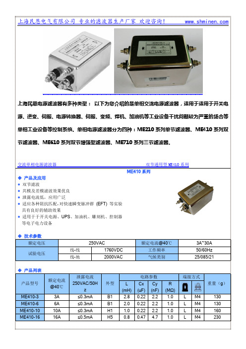
1.0 65 0.47 4.7 1.0
G2 0.5 40 1.0 4.7 1.0
G2 0.4 30 2.2 10 0.47
G2 0.3 20 2.2 10 0.47
N10 0.25 15 4.4 20 0.47
ME710-100 100A
≤2.0mA
N10 0.2 15 4.4 20 0.47
电源滤波器是一种无源低通滤波器,滤波频段在 10KHz-30MHz 之间,不仅能有效抑制沿电源线传播的传导 干扰,同时也能大大降低电子设备产生的辐射干扰。
滤波器命名说明
ME 210 D – 10 / ??
端接方式代号 Connection Type 额定电流数 Rated Current
附加位(可同时出现)/Option “D” 直流滤波器 / DC filter “H” 高工作电压型 / High voltage filter “M” 军用滤波器/ Military filter “B” 医用滤波器 / Medical filter “F” 400Hz 滤波器 / 400Hz filter “L” 低漏电流型 / Low leakage current filter “S” 小体积型 / Small size filter ......
◆ 技术参数 额定电压
试验电压
线-线 线-地
250VAC 1760VDC 2000VAC
额定电流@40℃ 工作频率 气候类别
1A~25A 50/60Hz 25/085/21
◆ 产品列表
产品型号
ME610-1 ME610-3 ME610-6 ME610-10 ME610-16 ME610-25
额定电流 @40℃
● 适用于逆变、伺服、变频、焊机、加油机等工业设
Fuji 4112 4127 数码多功能机 产品手册

Fuji Xerox®4112™4127™产品介绍快速,灵活,而且操作简单。
Fuji Xerox 4112™/4127™数码多功能机帮助您实现业务增长。
您可以用它来扩展业务范围,吸引更多客户,从而提高营收。
它功能丰富,操作简单。
能制作独特新颖,复杂、灵活多样的文档,快速且专业,生产力强,也可以满足各特定行业的客户应用。
如您所需,我们的数码多功能机为您提供:高速打印,高达每分钟125页—是同级别机器中最快的—和每分钟110页两款。
高速复印/扫描,每分钟可达100面的单面/双面原稿扫描速度。
两种强大的打印服务器,包括技术先进功能丰富的集成式打印控制器专为满足您的个性化需求而设计。
特别强大的生产力,使您可以在较短的打印时间内集中完成大批量打印。
操作简单—每个人都可以轻松使用。
•优异的图像质量和输出套准精度。
多种在线装订选择,扩展您的文件生产功能。
可增加的进纸点和可选配的各种纸张处理设备,不仅提高生产力,而且让您的产品出类拔萃。
值得信赖的品质。
占地面积小,高性价比。
••EA 碳粉通过印出精细线条,来表现最高层次的图像细节,清晰的文本,半色调和实地效果。
EA 墨粉可以渲染出最复杂的线条和刀锋般的锐利效果。
同量的碳粉可打印更多的页面,减少加粉次数,降低对生产的干扰。
超长的感光鼓寿命,较低的碳粉用量,有助于环保。
创新的EA 碳粉技术,对我们数码多功能机的高成像质量起到了关键的作用:•••••••••••2高速,量产,高质量图像,又容易使用再紧迫的交货期也能轻松满足。
处理更多的工作而输出更快。
轻松创建高质量的输出。
让您的投资充分发挥价值。
4112™/4127™数码多功能机无与伦比的打印速度和生产效率,出色的画质和易于使用,达到您的目标并更符合您的要求。
高速打印引擎使每分钟的输出高达125页和110页。
单路径、双扫描头扫描器无论扫描单面还是双面原稿,扫描速度都可达到每分钟100面。
同时扫描/接受,RIP ,并打印,提供最大的吞吐量。
半导体传感器AD7192BRUZ中文规格书

IDDO = IDDO (Q)
f ≤ 0.5 fr
IDDO = (IDDO (D) + (0.5 × 10⁻³) × CL × VDDO) × (2f − fr) + IDDO (Q) f > 0.5 fr
where: IDDI (D), IDDO (D) are the input and output dynamic supply currents per channel (mA/Mbps). CL is the output load capacitance (pF). VDDO is the output supply voltage (V). f is the input logic signal frequency (MHz); it is half of the input data rate expressed in units of Mbps. fr is the input stage refresh rate (Mbps). IDDI (Q), IDDO (Q) are the specified input and output quiescent supply currents (mA).
03786-014
PROPAGATION DELAY (ns)
Data Sheet
40
3V 35
30
5V
25
–50
–25
0
25
50
TEMPERATURE (°C)
75
100
Figure 16. Propagation Delay vs. Temperature, C Grade
03786-016
Rev. L | Page 26 of 31
54122中文资料

H e HIGH Voltage Level L e LOW Voltage Level X e Immaterial Input pins 1 and 2 are logically interchangeable as are input pins 3 and 4
3
元器件交易网
The ’122 features positive and negative DC level triggering inputs complementary outputs an optional 10 kX internal timing resistor and an overriding Direct Clear (CD) input When the circuit is in the quasi-stable (delay) state another trigger applied to the inputs (per Truth Table) will cause the delay period to start again without disturbing the outputs This process can be repeated indefinitely and thus the output pulse period (Q HIGH Q LOW) can be made as long as desired Alternatively a delay period can be terminated by a LOW signal applied to CD which also prevents triggering An internal connection from CD to the input gate makes it possible to trigger the circuit by a positive-going signal on CD as shown in the Truth Table For timing capacitor values greater than 1000 pF the output pulse width is defined as follows tw e 0 32 RXCX (1 0 a 0 7 RX) Where tw is in ns RX is in kX and CX is in pF
ADF4110中文数据手册

班级040831学号04083104本科毕业设计(论文)外文资料翻译毕业设计题目大功率对讲机接收电路的设计外文资料题目ADF4110系列芯片数据手册学院机电工程学院专业自动化学生姓名庄伟源指导教师姓名李西安ADF4110系列芯片手册 1RF PLL频率合成器ADF4110、ADF4111、ADF4112、ADF4112特征ADF4110: 550 MHzADF4111: 1.2 GHzADF4112: 3.0 GHzADF4113: 4.0 GHz2.7 V到5.5 V电源独立的电荷泵电源(VP)允许扩展调谐电压,3 V系统可编程双模分频器8/9, 16/17,32/33, 64/65可编程电荷泵电流可编程Antibacklash脉宽3-Wire串行接口模拟和数字锁定检测硬件和软件关断模式应用无线电台(GSM, PCS, DCS,基站CDMA,的WCDMA)无线手机(GSM, PCS, DCS, CDMA,的WCDMA)无线LANS通信测试设备CATV设备概述该频率合成器可用于ADF4110 系列实施的上变频和下本振,无线接收器和发射器变频部分.他们由一个低噪声数字PFD(相位频率检测器),一个精密电荷泵,一个可编程参考分频器,可编程A和B计数器和一个双模预置分频器性(P / P+1).在A (6-bit)和B (13-bit)柜台,联与双模分频器性(P / P+1),实现一N 分(N = BP + A).此外,14-bit引用计数器(R柜),允许在PFD将REFIN频率可选输入.如果使用合成器与外部环路滤波器和VCO(压控振荡器)可以实现一个完整的PLL(锁相环)。
所有片内寄存器的控制是通过一个简单的3-wire接口。
该器件采用功率范围从2.7 V供应5.5 V和断电时,可在不使用.功能框图对应部分翻译:14-bit R counter 14位R计数器;REFERENCE 基准;PHASE FREQUENCY DETECTOR 鉴频鉴相器;CHARGE PUMP 充电泵;R COUNTER LATCH R计数器锁存;24-BIT INPUT REGISTER 24位输入寄存器;FUNCTION LATCH 功能锁存;A, B COUNTER LATCH A、B计数器锁存;LOCK DETECT 锁定检测;CURRENT SETTING 1 电流设置1;CURRENT SETTING 2 电流设置2;ADF4110系列芯片手册2FROM FUNCTION LATCH 来自功能锁存; PRESCALER P/P +1 前置分频器P/P+1; 13-BIT B COUNTER 13位B 计数器;REV:由ADI 公司提供的信息被认为是准确和可靠.但是,没有承担责任的模拟装置 使用,也没有侵犯任何专利或其它第三方权利这可能是由于它的使用.没有获发牌照以暗示或否则根据ADI 公司的任何专利或专利的权利.其中技术的方式,P.O.盒9106,诺伍德,MA 02062-9106, U.S.A. 电话:781/329-4700万维网网址: 传真:781/326-8703 ©模拟装置,Inc., 2000ADF4110系列芯片手册 3ADF4110/ADF4111/ADF4112/ADF4113——规格(AVDD = DVDD = 3 V 10%, 5 V 10%; AVDD ≤ VP ≤ 6.0 V; AGND = DGND = CPGND = 0 V; RSET = 4.7 k ; TA = TMIN to TMAX 除非额外注释)参数B电压B夹单位测试条件/评论RF特征(3 V)RF输入频率ADF4110ADF4110ADF4111ADF4112ADF4112ADF4113RF输入灵敏度最大允许预分频器输出频率33RF特征(5 V)RF输入频率ADF4110ADF4111ADF4112ADF4113ADF4113RF输入灵敏度最大允许预分频器输出频率45/55025/5500.045/1.20.2/3.00.1/3.00.2/3.7–15/016525/5500.025/1.40.1/3.00.2/3.70.2/4.0–10/020045/55025/5500.045/1.20.2/3.00.1/3.00.2/3.7–15/016525/5500.025/1.40.1/3.00.2/3.70.2/4.0–10/0200MHz最小/最大MHz最小/最大GHz最小/最大GHz最小/最大GHz最小/最大GHz最小/最大dBm最小/最大MHz 最大MHz最小/最大GHz最小/最大GHz最小/最大GHz最小/最大GHz最小/最大dBm最小/最大MHz 最大参见图输入电路25.使用低频率的方波输入电平= –10 dBm输入电平= –10 dBm输入电平= –10 dBm使用低频率的方波.输入电平= –5 dBm将REFIN特征将REFIN输入频率参考输入灵敏度4输入电容将REFIN将REFIN输入电流0/100–5/010±1000/100–5/010±100MHz最小/最大dBm最小/最大pF 最大µA最大交流耦合.当直流耦合:0到V DD最大(CMOS兼容)鉴相器鉴相器频率55555MHz 最大电荷泵I CP吸入/源高价值低值绝对精度R SET范围56252.52.7/1056252.52.7/10mA typµAtyp% typkΩ typ可编程:见表V随着R SET= 4.7 kΩ随着R SET= 4.7 kΩ见表VADF4110系列芯片手册4I CP3-State泄漏电流汇和源电流匹配I CP主场迎战V CPI CP与温度的关系121.52121.52nA typ% typ% typ% typ0.5 V≤V CP≤V P– 0.50.5 V≤V CP≤V P– 0.5V CP= V P/2逻辑输入V INH,输入高电压V INL,输入低电压I INH/I INL,输入电流C IN,输入电容0.8×DV DD0.2×DV DD±1100.8×DV DD0.2×DV DD±110V 最小V 最大µA最大pF 最大逻辑输出V OH,输出高电压V OL,输出低电压DV DD– 0.40.4DV DD– 0.40.4V 最小V 最大I OH= 500µAI OL= 500µA电力用品AV DDDV DDV PI DD6(AI DD+ DI DD) ADF4110ADF4111ADF4112ADF4113I P低功耗的睡眠模式2.7/5.5AV DDAV DD/6.05.55.57.5110.512.7/5.5AV DDAV DD/6.05.55.57.5110.51V分钟/视频最大V分钟/视频最大mA 最大mA 最大mA 最大mA 最大mA 最大µAtypAV DD≤V P≤6.0 V见图22和234.5 mA典型4.5 mA典型6.5 mA典型8.5 mA典型T A= 25°C噪声特性ADF4113相位噪声楼7相位噪声性能8ADF4110: 540 MHz输出9 ADF4111: 900 MHz输出10 ADF4112: 900 MHz输出10 ADF4113: 900 MHz输出10 ADF4111: 836 MHz输出11 ADF4112: 1750 MHz输出12 ADF4112: 1750 MHz输出13 ADF4112: 1960 MHz输出14 ADF4113: 1960 MHz输出14 ADF4113: 3100 MHz输出15杂散信号–171–164–91–87–90–91–78–86–66–84–85–86–171–164–91–87–90–91–78–86–66–84–85–86dBc/Hz typdBc/Hz typdBc/Hz typdBc/Hz typdBc/Hz typdBc/Hz typdBc/Hz typdBc/Hz typdBc/Hz typdBc/Hz typdBc/Hz typdBc/Hz typ@ 25千赫频率PFD@ 200千赫频率PFD@ VCO输出@ 1 kHz偏移和200千赫频率PFD@ 1 kHz偏移和200千赫频率PFD@ 1 kHz偏移和200千赫频率PFD@ 1 kHz偏移和200千赫频率PFD@ 300 Hz失调和30千赫频率PFD@ 1 kHz偏移和200千赫频率PFD@ 200 Hz失调和10千赫频率PFD@ 1 kHz偏移和200千赫频率PFD@ 1 kHz偏移和200千赫频率PFD@ 1 kHz偏移频率和1 MHz PFDADF4110系列芯片手册 5ADF4110: 540 MHz输出9 ADF4111: 900 MHz输出10 ADF4112: 900 MHz输出10 ADF4113: 900 MHz输出10 ADF4111: 836 MHz输出11 ADF4112: 1750 MHz输出12 ADF4112: 1750 MHz输出13 ADF4112: 1960 MHz输出14 ADF4113: 1960 MHz输出14 ADF4113: 3100 MHz输出15–97/–106–98/–110–91/–100–100/–110–81/–84–88/–90–65/–73–80/–84–80/–84–80/–82–97/–106–98/–110–91/–100–100/–110–81/–84–88/–90–65/–73–80/–84–80/–84–80/–82dBc typdBc typdBc typdBc typdBc typdBc typdBc typdBc typdBc typdBc typ@ 200千赫/ 400 kHz和200千赫频率PFD@ 200千赫/ 400 kHz和200千赫频率PFD@ 200千赫/ 400 kHz和200千赫频率PFD@ 200千赫/ 400 kHz和200千赫频率PFD@ 30千赫/ 60 kHz和30千赫频率PFD@ 200千赫/ 400 kHz和200千赫频率PFD@ 10千赫/ 20 kHz和10千赫频率PFD@ 200千赫/ 400 kHz和200千赫频率PFD@ 200千赫/ 400 kHz和200千赫频率PFD@ 1 MHz/2 MHz和1 MHz PFD频率附注:1工作温度范围为如下:B版:-40°C至+85°C。
半导体传感器ADF7901BRUZ中文规格书

–2–AD626–SPECIFICATIONS ModelAD626A AD626B Parameter Condition Min T yp Max Min T yp Max Unit GAINGain Accuracy T otal ErrorGain = 10@ V OUT ≥ 100 mV dc0.4 1.00.2 0.6 % Gain = 100@ V OUT ≥ 100 mV dc0.1 1.00.5 0.6 %Over T emperature, T A = T MIN to T MAX G = 105030 ppm/°C G = 100150120 ppm/°C Gain LinearityGain = 10@ V OUT ≥ 100 mV dc0.014 0.0160.014 0.016 % Gain = 100@ V OUT ≥ 100 mV dc0.014 0.020.014 0.02 %OFFSET VOLTAGEInput Offset Voltage1.92.5 1.9 2.5 mV vs. T emperatureT MIN to T MAX , G = 10 or 100 2.9 2.9 mV vs. T emperatureT MIN to T MAX , G = 10 or 1006 6 µV/°C vs. Supply Voltage (PSR)+PSR74 80 74 80 dB –PSR64 66 64 66 dB COMMON-MODE REJECTIONR L = 10 k ⍀+CMR Gain = 10, 100f = 100 Hz, V CM = +24 V 66 90 80 90 dB ±CMR Gain = 10, 100f = 10 kHz, V CM = +6 V 55 64 55 64 dB –CMR Gain = 10, 100*f = 100 Hz, V CM = –2 V 60 85 73 85 dB COMMON-MODE VOLTAGE RANGE+CMV Gain = 10CMR > 85 dB +24+24V –CMV Gain = 10CMR > 85 dB –2–2V INPUTInput ResistanceDifferential200 200 k ⍀ Common-Mode100 100 k ⍀ Input Voltage Range (Common-Mode)6 (V S – l) 6 (V S – l) V OUTPUTOutput Voltage SwingR L = 10 k ⍀ PositiveGain = 10 4.7 4.90 4.7 4.90 V Gain = 100 4.7 4.90 4.7 4.90 V NegativeGain = 100.03 0.03 V Gain = 1000.03 0.03 V Short Circuit Current+I SC12 12 mA NOISEVoltage Noise RTIGain = 10f = 0.1 Hz–10 Hz 2 2 µV p-p Gain = 100f = 0.1 Hz–10 Hz 2 2 µV p-p Gain = 10f = 1 kHz 0.25 0.25 µV/ͱHz Gain = 100f = 1 kHz 0.25 0.25 µV/ͱHz DYNAMIC RESPONSE–3 dB BandwidthV OUT = +1 V dc 100 100 kHz Slew Rate, T MIN to T MAXGain = 100.17 0.22 0.17 0.22 V/µs Gain = 1000.1 0.17 0.1 0.17 V/µs Settling Timeto 0.01%, 1 V Step 24 22 µs POWER SUPPLYOperating RangeT A = T MIN to T MAX 2.4 5 12 2.4 5 10 V Quiescent CurrentGain = 100.16 0.20 0.16 0.20 mA Gain = 1000.23 0.290.23 0.29 mATRANSISTOR COUNT Number of Transistors 46 46*At temperatures above 25°C, –CMV degrades at the rate of 12 mV/°C; i.e., @ 25°C CMV = –2 V, @ 85°C CMV = –1.28 V .Specifi cations subject to change without notice.(@+V S = +5 V and T A = 25؇C, un l ess oth e r w ise noted.)SINGLE SUPPLYREV. DAD626–10–necessary to min i m ize gain error. Also, any mis m atch be t ween the total source re s is t ance at each input will af f ect gain ac c u r a c y and common -mode rejection (CMR). For ex a m p le: when operating at a gain of 10, an 80 ⍀ mismatch in the source re s is t ance between the inputs will degrade CMR to 68 dB.The output buffer, A2, operates at a gain of 2 or 20, thus setting the overall, precalibrated gain of the AD626 (with no ex t er n al com p o n ents) at 10 or 100. The gain is set by the feedback net w ork around amplifi er A2.The output of amplifi er A2 relies on a 10 k ⍀ resistor to –V S for “pull-down.” For single-supply operation, (–V S = “GND”), A2 can drive a 10 k ⍀ ground ref e r e nced load to at least +4.7 V . The min i m um, nominally “zero,” output voltage will be 30 mV . For dual-supply op e r a t ion (±5 V), the positive output voltage swing will be the same as for a single supply. The negative swing will be to –2.5 V, at G = 100, limited by the ratio:–V R R R R R S ×+++1514131415 T he negative range can be extended to –3.3 V (G = 100) and –4 V (G = 10) by add i ng an external 10 k ⍀ pull-down from the out p ut to –V S . This will add 0.5 mA to the AD626’s qui e s c ent cur r ent, bringing the total to 2 mA.The AD626’s 100 kHz bandwidth at G = 10 and 100 (a 10 MHzgain bandwidth) is much higher than can be obtained with low power op amps in discrete dif f er e n t ial amplifi er circuits. Fur t her -more, the AD626 is stable driving capacitive loads up to 50 pF (G10) or 200 pF (G100). Capacitive load drive can be increased to 200 pF (G10) by connecting a 100 ⍀ resistor in series with the AD626’s output and the load.ADJUSTING THE GAIN OF THE AD626The AD626 is easily confi gured for gains of 10 or 100. Figure 5 shows that for a gain of 10, Pin 7 is simply left un c on n ect e d; simi-larly, for a gain of 100, Pin 7 is grounded, as shown in Fig u re 6.Gains between 10 and 100 are easily set by connecting a vari a ble resistance between Pin 7 and Analog GND, as shown in Fig u re 7. Because the on-chip resistors have an absolute tol e r a nce of ±20% (although they are ratio matched to within 0.1%), at least a 20% adjustment range must be provided. The values shown in the table in Figure 7 provide a good trade-off be t ween gain set range and resolution, for gains from 11 to 90.S –INPUT –V Figure 5.AD626 Confi gured for a Gain of 10–INPUT S –V Figure 6. AD626 Confi gured for a Gain of 100–INPUT CORNER FREQUENCY OF FILTER =12CF (100k ⍀)GAIN RANGE R G (⍀) R H (⍀)11 – 2020 – 4040 – 8080 – 100100k10k1k100 4.99k 802802RESISTOR VALUES FOR GAIN ADJUSTMENT Figure 7. Recommended Circuit for Gain Adjustment SINGLE-POLE LOW-PASS FILTERING A low-pass fi lter can be easily implemented by using the fea t ures provided by the AD626.By simply connecting a capacitor between Pin 4 and ground, a single-pole low-pass fi lter is created, as shown in Figure 8.CORNER FREQUENCY OF FILTER =12CF (100k ⍀)OUTPUT –INPUT Figure 8. A One-Pole Low-Pass Filter CircuitWhich Operates from a Single +10 V SupplyREV. D。
半导体传感器ADG1606BRUZ中文规格书

ADF4116/ADF4117/ADF4118Rev. D | Page 20 of 28• Fastlock Mode 2 uses the values in the timer counter to determine the timeout period before reverting to normal mode operation after fastlock. Fastlock Mode 2 is chosen by setting DB11 to 1. • The user must also decide how long to keep the high current (1 mA) active before reverting to low current (250 μA). This is controlled by the timer counter control bits, DB14 to DB11 (TC4 to TC1), in the function latch. The truth table is given in Figure 33. • To program a new output frequency, program the A counter and B counter latch with new values for A and B. At the same time, set the CP Gain bit to a 1, which sets the chargepump to 1 mA for a period of time determined by TC4 to TC1. When this time is up, the charge pump currentreverts to 250 μA. At the same time, the CP Gain bit in theA counter andB counter latch is reset to 0 and is ready for the next time that the user wants to change the frequency. INITIALIZATION LATCH When C2 and C1 are both set to 1, the initialization latch is programmed. This is essentially the same as the function latch that is programmed when C2, C1 = 1, 0. However, when the initialization latch is programmed, an additional internal reset pulse is applied to the R counter and N counter. This pulse ensures that the N counter is at a load point when the N counter data is latched and that the device begins counting in close phase alignment. If the latch is programmed for synchronous power-down (CE pin is high; PD1 bit is high; PD2 bit is low), the internal pulse also triggers this power-down. The prescaler reference and the oscillator input buffer are unaffected by the internal reset pulse,so close phase alignment is maintained when counting resumes. When the first N counter data is latched after initialization, the internal reset pulse is again activated. However, successive N counter loads do not trigger the internal reset pulse. DEVICE PROGRAMMING AFTER INITIAL POWER-UP After initial power-up, the device can be programmed by the initialization latch method, the CE pin method, or the counter reset method. Initialization Latch Method 1. Apply V DD . 2. Program the initialization latch (11 in 2 LSBs of input word). Make sure that F1 bit is programmed to 0. 3. Do an R load (00 in 2 LSBs).4. Do an N load (01 in 2 LSBs).When the initialization latch is loaded, the following occurs: •The function latch contents are loaded. • An internal pulse resets the R, N, and timeout counters toload state conditions and also three-states the charge pump. Note that the prescaler band gap reference and the oscillator input buffer are unaffected by the internal reset pulse, allowing close phase alignment when counting resumes.• Latching the first N counter data after the initialization word activates the same internal reset pulse. Successive N loads do not trigger the internal reset pulse unless there is another initialization. CE Pin Method 1. Apply V DD . 2. Bring CE low to put the device into power-down. This is anasynchronous power-down in that it happens immediately.3. Program the function latch (10).4. Program the R counter latch (00).5. Program the N counter latch (01).6. Bring CE high to take the device out of power-down. The R counter and N counter resume counting in close alignment. Note that after CE goes high, a duration of 1 μs may be required for the prescaler band gap voltage and oscillator input buffer bias to reach a steady state.CE can be used to power up and power down the device to check for channel activity. The input register does not need to be repro-grammed each time the device is disabled and enabled, as long as it is programmed at least once after V CC is initially applied. Counter Reset Method 1. Apply V DD .2. Do a function latch load (10 in 2 LSBs). As part of this,load 1 to the F1 bit. This enables the counter reset.3. Do an R counter load (00 in 2 LSBs).4. Do an N counter load (01 in 2 LSBs).5. Do a function latch load (10 in 2 LSBs). As part of this,load 0 to the F1 bit. This disables the counter reset.This sequence provides the same close alignment as the initiali-zation method. It offers direct control over the internal reset. Note that counter reset holds the counters at load point and three-states the charge pump, but it does not trigger synchro-nous power-down. The counter reset method requires an extra function latch load compared to the initialization latch method.ADF4116/ADF4117/ADF4118Rev. D | Page 22 of 28ΩΩOUT F REFIN Ω.00392-035Figure 35. Local Oscillator for GSM Base Station ΩΩRF OUTF REFIN BEEN OMITTED FROM THE DIAGRAM FOR CLARITY.00392-036Figure 36. Local Oscillator Shutdown Circuit。
- 1、下载文档前请自行甄别文档内容的完整性,平台不提供额外的编辑、内容补充、找答案等附加服务。
- 2、"仅部分预览"的文档,不可在线预览部分如存在完整性等问题,可反馈申请退款(可完整预览的文档不适用该条件!)。
- 3、如文档侵犯您的权益,请联系客服反馈,我们会尽快为您处理(人工客服工作时间:9:00-18:30)。
RF PLL Frequency SynthesizersADF4110/ADF4111/ADF4112/ADF4113Rev. CInformation furnished by Analog Devices is believed to be accurate and reliable. However, no responsibility is assumed by Analog Devices for its use, nor for any infringements of patents or other rights of third parties that may result from its use. Specifications subject to change without notice. No license is granted by implication or otherwise under any patent or patent rights of Analog Devices. Trademarks and registered trademarks are the property of their respective owners.One Technology Way, P.O. Box 9106, Norwood, MA 02062-9106, U.S.A. Tel: 781.329.4700 Fax: 781.326.8703© 2004 Analog Devices, Inc. All rights reserved.FEATURESADF4110: 550 MHz; ADF4111: 1.2 GHz; ADF4112: 3.0 GHz; ADF4113: 4.0 GHz2.7 V to 5.5 V power supplySeparate charge pump supply (V P ) allows extended tuning voltage in 3 V systemsProgrammable dual-modulus prescaler 8/9, 16/17, 32/33, 64/65Programmable charge pump currents Programmable antibacklash pulse width 3-wire serial interfaceAnalog and digital lock detectHardware and software power-down modeAPPLICATIONSBase stations for wireless radio (GSM, PCS, DCS, CDMA, WCDM A)Wireless handsets (GSM, PCS, DCS, CDMA, WCDMA) Wireless LANSCommunications test equipment CATV equipmentGENERAL DESCRIPTIONThe ADF4110 family of frequency synthesizers can be used to implement local oscillators in the upconversion and downcon-version sections of wireless receivers and transmitters. They consist of a low noise digital PFD (phase frequency detector), a precision charge pump, a programmable reference divider,programmable A and B counters, and a dual-modulus prescaler (P/P + 1). The A (6-bit) and B (13-bit) counters, in conjunction with the dual-modulus prescaler (P/P + 1), implement an N divider (N = BP + A). In addition, the 14-bit reference counter (R counter) allows selectable REFIN frequencies at the PFD input. A complete phase-locked loop (PLL) can be implemented if the synthesizer is used with an external loop filter and voltage controlled oscillator (VCO).Control of all the on-chip registers is via a simple 3-wireinterface. The devices operate with a power supply ranging from 2.7 V to 5.5 V and can be powered down when not in use.FUNCTIONAL BLOCK DIAGRAMRF IN RF IN LEREF MUXOUTCPR 03496-0-001Figure 1. Functional Block DiagramADF4110/ADF4111/ADF4112/ADF4113Rev. C | Page 2 of 28TABLE OF CONTENTSSpecifications.....................................................................................3 Timing Characteristics.....................................................................5 Absolute Maximum Ratings............................................................6 Transistor Count...........................................................................6 ESD Caution..................................................................................6 Pin Configurations and Function Descriptions...........................7 Typical Performance Characteristics.............................................8 Circuit Description.........................................................................12 Reference Input Section.............................................................12 RF Input Stage.............................................................................12 Prescaler (P/P + 1)......................................................................12 A and B Counters.......................................................................12 R Counter....................................................................................12 Phase Frequency Detector (PFD) and Charge Pump............13 Muxout and Lock Detect...........................................................13 Input Shift Register....................................................................13 Function Latch............................................................................19 Initialization Latch.....................................................................20 Device Programming after Initial Power-Up.........................20 Resynchronizing the Prescaler Output....................................21 Applications.....................................................................................22 Local Oscillator for GSM Base Station Transmitter..............22 Using a D/A Converter to Drive the R SET Pin.........................23 Shutdown Circuit.......................................................................23 Wideband PLL............................................................................23 Direct Conversion Modulator..................................................25 Interfacing...................................................................................26 PCB Design Guidelines for Chip Scale Package....................26 Outline Dimensions.......................................................................27 Ordering Guide. (28)REVISION HISTORY3/04—Data sheet changed from Rev. B to Rev. C.Updated Format..............................................................Universal Changes to Specifications............................................................2 Changes to Figure 32..................................................................22 Changes to the Ordering Guide................................................28 3/03—Data sheet changed from Rev. A to Rev. B.Edits to Specifications..................................................................2 Updated OUTLINE DIMENSIONS........................................24 1/01—Data sheet changed from Rev. 0 to Rev. A.Changes to DC Specifications in B Version, B Chips,Unit, and Test Conditions/Comments Columns.................2 Changes to Absolute Maximum Rating.....................................4 Changes to FR IN A Function Test................................................5 Changes to Figure 8......................................................................7 New Graph Added—TPC 22.......................................................9 Change to PD Polarity Box in Table V.....................................15 Change to PD Polarity Box in Table VI...................................16 Change to PD Polarity Paragraph............................................17 Addition of New Material(PCB Design Guidelines for Chip–Scale package)...........23 Replacement of CP-20 Outline with CP-20 [2] Outline.. (24)ADF4110/ADF4111/ADF4112/ADF4113Rev. C | Page 3 of 28SPECIFICATIONSAV DD = DV DD = 3 V ± 10%, 5 V ± 10%; AV DD ≤V P ≤ 6.0 V; AGND = DGND = CPGND = 0 V; R SET = 4.7 kΩ; dBm referred to 50 Ω; T A =T MIN to T MAX , unless otherwise noted. Operating temperature range is as follows: B Version: −40°C to +85°C. Table 1.ParameterB Version B Chips 1 Unit Test Conditions/Comments RF CHARACTERISTICS (3 V)See Figure 29 for input circuit. RF Input Sensitivity −15/0 −15/0 dBm min/max RF Input FrequencyADF411080/550 80/550 MHz min/maxFor lower frequencies, ensure slew rate (SR) > 30 V/µs.ADF4110 50/550 50/550 MHz min/max Input level = −10 dBm. ADF4111 0.08/1.2 0.08/1.2 GHz min/max For lower frequencies, ensure SR > 30 V/µs. ADF4112 0.2/3.0 0.2/3.0 GHz min/max For lower frequencies, ensure SR > 75 V/µs. ADF4112 0.1/3.0 0.1/3.0 G Hz min/max Input level = −10 dBm. ADF4113 0.2/3.7 0.2/3.7 G Hzmin/max Input level = −10 dBm. For lower frequencies, ensure SR > 130 V/µs. Maximum Allowable Prescaler OutputFrequency 2165 165 MHz max RF CHARACTERISTICS (5 V) RF Input Sensitivity −10/0 −10/0 dBm min/max RF Input Frequency ADF4110 80/550 80/550 MHz min/max For lower frequencies, ensure SR > 50 V/µs.ADF4111 0.08/1.4 0.08/1.4 GHz min/max For lower frequencies, ensure SR > 50 V/µs.ADF4112 0.1/3.0 0.1/3.0 GHz min/max For lower frequencies, ensure SR > 75 V/µs. ADF4113 0.2/3.7 0.2/3.7 GHz min/max For lower frequencies, ensure SR > 130 V/µs. ADF4113 0.2/4.0 0.2/4.0 G Hz min/max Input level = −5 dBmMaximum Allowable Prescaler OutputFrequency 2200 200 MHz max REFIN CHARACTERISTICS REFIN Input Frequency 5/104 5/104 MHz min/max For f < 5 MHz, ensure SR > 100 V/µs. Reference Input Sensitivity 0.4/AV DD 0.4/AV DD V p-p min/max AV DD = 3.3 V, biased at AV DD /2. See Note 3. 3.0/AV DD 3.0/AV DD V p-p min/max AV DD = 5 V, biased at AV DD /2. See Note 3. REFIN Input Capacitance 10 10 pF max REFIN Input Current ±100 ±100 µA maxPHASE DETECTOR FREQUENCY 455 55 MHz max CHAR GE PUMP I CP Sink/Source Programmable (see Table 9). High Value 5 5 mA typ With R SET = 4.7 kΩ Low Value 625 625 µA typ Absolute Accuracy 2.5 2.5 % typ With R SET = 4.7 kΩ R SET Range 2.7/10 2.7/10 kΩ typ See Table 9. I CP 3-State Leakage Current 1 1 nA typ Sink and Source Current Matching 2 2 % typ 0.5 V ≤ V CP ≤ V P – 0.5 V. I CP vs. V CP 1.5 1.5 % typ 0.5 V ≤ V CP ≤ V P – 0.5 V. I CP vs. Temperature 2 2 % typ V CP = V P /2. LOGIC INPUTS V INH , Input High Voltage 0.8 × DV DD 0.8 × DV DD V min V INL , Input Low Voltage 0.2 × DV DD 0.2 × DV DD V max I INH /I INL , Input Current ±1 ±1 µA max C IN , Input Capacitance 10 10 pF max LOG IC OUTPUTS V OH , Output High Voltage DV DD – 0.4 DV DD – 0.4 V minI OH = 500 µA. V OL , Output Low Voltage 0.4 0.4 V max I OL = 500 µA.ADF4110/ADF4111/ADF4112/ADF4113Rev. C | Page 4 of 28Parameter B Version B Chips 1 Unit Test Conditions/CommentsPOWER SUPPLIES AV DD 2.7/5.5 2.7/5.5 V min/V max DV DD AV DD AV DDV P AV DD /6.0 AV DD /6.0 V min/V max AV DD ≤ V P ≤ 6.0 V. See Figure 25 and Figure 26. I DD 5(AI DD + DI DD ) ADF4110 5.5 4.5 mA max 4.5 mA typical ADF4111 5.5 4.5 mA max 4.5 mA typical ADF4112 7.5 6.5 mA max 6.5 mA typical ADF4113 11 8.5 mA max 8.5 mA typical I P 0.5 0.5 mA max T A = 25°C Low Power Sleep Mode 1 1 µA typ NOISE CHARACTERISTICSADF4113 Normalized Phase Noise Floor 6−215 −215 dBc/Hz typPhase Noise Performance 7@ VCO outputADF4110: 540 MHz Output 8−91 −91 dBc/Hz typ@ 1 kHz offset and 200 kHz PFD frequency ADF4111: 900 MHz Output 9−87 −87 dBc/Hz typ@ 1 kHz offset and 200 kHz PFD frequency ADF4112: 900 MHz Output 9−90 −90 dBc/Hz typ@ 1 kHz offset and 200 kHz PFD frequency ADF4113: 900 MHz Output 9−91 −91 dBc/Hz typ @ 1 kHz offset and 200 kHz PFD frequency ADF4111: 836 MHz Output 10 −78 −78 dBc/Hz typ@ 300 Hz offset and 30 kHz PFD frequency ADF4112: 1750 MHz Output 11−86 −86 dBc/Hz typ@ 1 kHz offset and 200 kHz PFD frequency ADF4112: 1750 MHz Output 12−66 −66 dBc/Hz typ @ 200 Hz offset and 10 kHz PFD frequency ADF4112: 1960 MHz Output 13 −84 −84 dBc/Hz typ@ 1 kHz offset and 200 kHz PFD frequency ADF4113: 1960 MHz Output 13−85 −85 dBc/Hz typ@ 1 kHz offset and 200 kHz PFD frequency ADF4113: 3100 MHz Output 14−86 −86 dBc/Hz typ @ 1 kHz offset and 1 MHz PFD frequency Spurious SignalsADF4110: 540 MHz Output 9−97/−106 −97/−106 dBc typ@ 200 kHz/400 kHz and 200 kHz PFD frequency ADF4111: 900 MHz Output 9−98/−110 −98/−110 dBc typ @ 200 kHz/400 kHz and 200 kHz PFD frequency ADF4112: 900 MHz Output 9 −91/−100 −91/−100 dBc typ@ 200 kHz/400 kHz and 200 kHz PFD frequency ADF4113: 900 MHz Output 9−100/−110 −100/−110 dBc typ@ 200 kHz/400 kHz and 200 kHz PFD frequency ADF4111: 836 MHz Output 10−81/−84 −81/−84 dBc typ@ 30 kHz/60 kHz and 30 kHz PFD frequency ADF4112: 1750 MHz Output 11−88/−90 −88/−90 dBc typ@ 200 kHz/400 kHz and 200 kHz PFD frequency ADF4112: 1750 MHz Output 12−65/−73 −65/−73 dBc typ@ 10 kHz/20 kHz and 10 kHz PFD frequency ADF4112: 1960 MHz Output 13−80/−84 −80/−84 dBc typ@ 200 kHz/400 kHz and 200 kHz PFD frequency ADF4113: 1960 MHz Output 13−80/−84 −80/−84 dBc typ@ 200 kHz/400 kHz and 200 kHz PFD frequency ADF4113: 3100 MHz Output 14−80/−82 −82/−82 dBc typ @ 1 MHz/2 MHz and 1 MHz PFD frequency1The B chip specifications are given as typical values.2This is the maximum operating frequency of the CMOS counters. The prescaler value should be chosen to ensure that the RF input is divided down to a frequency that is less than this value. 3AC coupling ensures AV DD /2 bias. See Figure 33 for a typical circuit. 4Guaranteed by design. 5T A = 25°C; AV DD = DV DD = 3 V; P = 16; SYNC = 0; DLY = 0; RF IN for ADF4110 = 540 MHz; RF IN for ADF4111, ADF4112, ADF4113 = 900 MHz. 6The synthesizer phase noise floor is estimated by measuring the in-band phase noise at the output of the VCO, PN TOT , and subtracting 20logN (where N is the N divider value) and 10logF PFD : PN SYNTH = PN TOT – 10logF PFD – 20logN. 7The phase noise is measured with the EVAL-ADF411xEB1 evaluation board and the HP8562E spectrum analyzer. The spectrum analyzer provides the REFIN for the synthesizer (f REFOUT = 10 MHz @ 0 dBm). SYNC = 0; DLY = 0 (Ta ). ble 78f REFIN = 10 MHz; f PFD = 200 kHz; offset frequency = 1 kHz; f RF = 540 MHz; N = 2700; loop B/W = 20 kHz. 9f REFIN = 10 MHz; f PFD = 200 kHz; offset frequency = 1 kHz; f RF = 900 MHz; N = 4500; loop B/W = 20 kHz. 10f REFIN = 10 MHz; f PFD = 30 kHz; offset frequency = 300 Hz; f RF = 836 MHz; N = 27867; loop B/W = 3 kHz. 11f REFIN = 10 MHz; f PFD = 200 kHz; offset frequency = 1 kHz; f RF = 1750 MHz; N = 8750; loop B/W = 20 kHz 12f REFIN = 10 MHz; f PFD = 10 kHz; offset frequency = 200 Hz; f RF = 1750 MHz; N = 175000; loop B/W = 1 kHz. 13f REFIN = 10 MHz; f PFD = 200 kHz; offset frequency = 1 kHz; f RF = 1960 MHz; N = 9800; loop B/W = 20 kHz. 14f REFIN = 10 MHz; f PFD = 1 MHz; offset frequency = 1 kHz; f RF = 3100 MHz; N = 3100; loop B/W = 20 kHz.ADF4110/ADF4111/ADF4112/ADF4113Rev. C | Page 5 of 28TIMING CHARACTERISTICSGuaranteed by design but not production tested. AV DD = DV DD = 3 V ± 10%, 5 V ± 10%; AV DD ≤ V P ≤ 6 V; AGND = DGND = CPGND = 0 V; R SET = 4.7 kΩ; T A = T MIN to T MAX , unless otherwise noted. Table 2.Parameter Limit at T MIN to T MAX (B Version) Unit Test Conditions/Comments t 1 10 ns min DATA to CLOCK setup time t 2 10 ns min DATA to CLOCK hold timet 3 25 ns min CLOCK high duration t 4 25 ns min CLOCK low duration t 5 10 ns min CLOCK to LE setup time t 620ns minLE pulse widthLELE03496-0-002Figure 2. Timing DiagramADF4110/ADF4111/ADF4112/ADF4113Rev. C | Page 6 of 28ABSOLUTE MAXIMUM RATINGST A = 25°C, unless otherwise notedTable 3.Parameter RatingAV DD to GND 1 −0.3 V to +7 VAV DD to DV DD −0.3 V to +0.3 VV P to GND −0.3 V to +7 VV P to AV DD −0.3 V to +5.5 V Digital I/O Voltage to GND −0.3 V to V DD + 0.3 V Analog I/O Voltage to GND −0.3 V to V P + 0.3 V REF IN , RF IN A, RF IN B to GND −0.3 V to V DD + 0.3 V RF IN A to RF IN B ±320 mVOperating Temperature RangeIndustrial (B Version) −40°C to +85°C Storage Temperature Range −65°C to +150°C Maximum Junction Temperature 150°C TSSOP θJA Thermal Impedance 150.4°C/W LFCSP θJA Thermal Impedance (Paddle Soldered)122°C/W LFCSP θJA Thermal Impedance(Paddle Not Soldered) 216°C/W Lead Temperature, Soldering Vapor Phase (60 sec) 215°C Infrared (15 sec) 220°C1GND = AGND = DGND = 0 V.Stresses above those listed under Absolute Maximum Ratings may cause permanent damage to the device. This is a stress rating only; functional operation of the device at these or anyother conditions above those listed in the operational sectionsof this specification is not implied. Exposure to absolutemaximum rating conditions for extended periods may affectdevice reliability. This device is a high performance RF integrated circuit with an ESD rating of <2 kV , and it is ESD sensitive. Proper precautions should be taken for handling and assembly. TRANSISTOR COUNT 6425 (CMOS) and 303 (Bipolar).ESD CAUTIONESD (electrostatic discharge) sensitive device. Electrostatic charges as high as 4000 V readily accumulate on the human body and test equipment and can discharge without detection. Although this product features proprietary ESD protection circuitry, permanent damage may occur on devices subjected to high energy electrostatic discharges. Therefore, proper ESD precautions are recommended to avoid performance degradation or loss of functionality.ADF4110/ADF4111/ADF4112/ADF4113Rev. C | Page 7 of 28PIN CONFIGURATIONS AND FUNCTION DESCRIPTIONSDD PR SET CP CPGND AGND RF IN B RF IN A AV DD REF IN03496-0-003CPGND AGNDAGND RF IN B RF IN AMUXOUT LE DATA CLK CEPS E TPV D DV D DA V D A V D R E F I D G N D G N 03496-0-004Figure 3. TSSOP Pin ConfigurationFigure 4. LFCSP Pin ConfigurationADF4110/ADF4111/ADF4112/ADF4113Rev. C | Page 8 of 28TYPICAL PERFORMANCE CHARACTERISTICSFREQ PARAM DATA KEYWORD IMPEDANCE–UNIT –TYPE –FORMAT–OHMS GHz S MA R 50FREQ MAGS11ANGS111.050.9512–40.1341.100.93458–43.7471.150.94782–44.3931.200.96875–46.9371.250.92216–49.61.300.93755–51.8841.350.96178–51.211.400.94354–53.551.450.95189–56.7861.500.97647–58.7811.550.98619–60.5451.600.95459–61.431.650.97945–61.2411.700.98864–64.0511.750.97399–66.191.800.97216–63.775FREQ MAGS11ANGS110.050.89207–2.05710.100.8886–4.44270.150.89022–6.32120.200.96323–2.13930.250.90566–12.130.300.90307–13.520.350.89318–15.7460.400.89806–18.0560.450.89565–19.6930.500.88538–22.2460.550.89699–24.3360.600.89927–25.9480.650.87797–28.4570.700.90765–29.7350.750.88526–31.8790.800.81267–32.6810.850.90357–31.5220.900.92954–34.2220.950.92087–36.9611.000.93788–39.34303496-0-005Figure 5. S-Parameter Data for the ADF4113 RF Input (up to 1.8 GHz)–35–30–25–20–15–10–50R F I N P U T P O W E R(d B m )012345RF INPUT FREQUENCY (GHz)03496-0-006Figure 6. Input Sensitivity (ADF4113)–100–90–80–70–60–50–40–30–20–100O U T P U TP O W E R (d B )–2.0kHz–1.0kHz900MHz 1.0kHz 2.0kHzFREQUENCY03496-0-007Figure 7 ADF4113 Phase Noise (900 MHz, 200 kHz, 20 kHz)–100–90–80–70–60–50–40–30–20–100O U T P U T P O W E R (d B )–2.0kHz–1.0kHz900MHz 1.0kHz 2.0kHzFREQUENCY03496-0-008Figure 8. ADF4113 Phase Noise(900 MHz, 200kHz, 20 kHz) with DLY and SYNC Enabled–140–130–120–110–100–90–80–70–60–50–40P H A S E N O I S E (d B c /H z )FREQUENCY OFFSET FROM 900MHz CARRIER (Hz)1k 10010k 100k 1M03496-0-009Figure 9. ADF4113 Integrated Phase Noise(900 MHz, 200 kHz, 20 kHz, Typical Lock Time: 400 µs)–140–130–120–110–100–90–80–70–60–50–40P H A S E N O I S E (d B c /H z )FREQUENCY OFFSET FROM 900MHz CARRIER (Hz)1k 10010k 100k 1M03496-0-010Figure 10. ADF4113 Integrated Phase Noise(900 MHz, 200 kHz, 35 kHz, Typical Lock Time: 200 µs)ADF4110/ADF4111/ADF4112/ADF4113Rev. C | Page 9 of 28–100–90–80–70–60–50–40–30–20–100O U T P U T P O W E R (d B )–400kHz–200kHz900MHz 200kHz 400kHzFREQUENCY03496-0-011Figure 11. ADF4113 Reference Spurs (900 MHz, 200 kHz, 20 kHz)–100–90–80–70–60–50–40–30–20–100O U T P U T P O W E R (d B )–400kHz–200kHz900MHz 200kHz 400kHzFREQUENCY03496-0-012Figure 12. ADF4113 (900 MHz, 200 kHz, 35 kHz)–100–90–80–70–60–50–40–30–20–100O U T P U T P O W E R (d B )–400Hz–200Hz1750MHz 200Hz 400HzFREQUENCY03496-0-013Figure 13. ADF4113 Phase Noise (1750 MHz, 30 kHz, 3 kHz) –140–130–120–110–100–90–80–70–60–50–40P H A S E N O I S E (d B c /H z )FREQUENCY OFFSET FROM 1750MHz CARRIER (Hz)1k10010k 100k 1M03496-0-014Figure 14. ADF4113 Integrated Phase Noise(1750 MHz, 30 kHz, 3 kHz)–100–90–80–70–60–50–40–30–20–100O U T P U T P O W E R (d B )FREQUENCY03496-0-015Figure 15. ADF4113 Reference Spurs (1750 MHz, 30 kHz, 3 kHz)–100–90–80–70–60–50–40–30–20–100O U T P U T P O W E R (dB )–2.0kHz–1.0kHz3100MHz 1.0kHz2.0kHzFREQUENCY03496-0-016Figure 16. ADF4113 Phase Noise (3100 MHz, 1 MHz, 100 kHz)ADF4110/ADF4111/ADF4112/ADF4113Rev. C | Page 10 of 28–140–130–120–110–100–90–80–70–60–50–40P H A S E N O I S E (d B c /H z )FREQUENCY OFFSET FROM 3100MHz CARRIER (Hz)10310210410510603496-0-017Figure 17. ADF4113 Integrated Phase Noise(3100 MHz, 1 MHz, 100 kHz)–100–90–80–70–60–50–40–30–20–100O U T P U T P O W E R (d B )–2.0MHz–1.0MHz3100MHz 1.0MHz2.0MHzFREQUENCY03496-0-018Figure 18. Reference Spurs (3100 MHz, 1 MHz, 100 kHz)–180–170–160–150–140–130–120P H A S E N O I S E (d B c /H z )PHASE DETECTOR FREQUENCY (kHz)10110010001000003496-0-019Figure 19. ADF4113 Phase Noise (Referred to CP Output)vs. Phase Detector Frequency P H A S E N O I S E (d B c /H z )–100–90–80–70–60–40–20020406080100TEMPERATURE (°C)03496-0-020Figure 20. ADF4113 Phase Noise vs. Temperature(900 MHz, 200 kHz, 20 kHz)F I R S T R E F E R E N C E S P U R (d B c )–100–90–80–70–60–40–20020406080100TEMPERATURE (°C)03496-0-021Figure 21. ADF4113 Reference Spurs vs. Temperature(900 MHz, 200 kHz, 20 kHz)–105–95–85–75–65–55–45–35–25–15–5F I R S T R E F E R E N C E S P U R (d B c )12345TUNING VOLT AGE (V)03496-0-022Figure 22. ADF4113 Reference Spurs (200 kHz) vs. V TUNE(900 MHz, 200 kHz, 20 kHz)P H A S E N O I S E (d B c /H z )–100–90–80–70–60–40–20020406080100TEMPERATURE (°C)03496-0-023Figure 23. ADF4113 Phase Noise vs. Temperature(836 MHz, 30 kHz, 3 kHz)F I R S T R E F E R E N C E S P U R (d B c )–100–90–80–70–60–40–2020406080100TEMPERATURE (°C)03496-0-024Figure 24. ADF4113 Reference Spurs vs. Temperature(836 MHz, 30 kHz, 3 kHz)012345678910A I D D (m A )PRESCALER VALUE8/916/1732/3364/6503496-0-025Figure 25. AI DD vs. Prescaler Value0.51.01.52.02.53.0DI D D (m A )PRESCALER OUTPUT FREQUENCY (MHz)50010015020003496-0-026Figure 26. DI DD vs. Prescaler Output Frequency (ADF4110, ADF4111, ADF4112, ADF4113)–6–4–2–3–50–1I C P (m A )21436500.5 1.0 1.5 2.0 2.5 3.0 3.5 4.0 4.5 5.0V CP (V)03496-0-027Figure 27. Charge Pump Output Characteristics for ADF4110 FamilyCIRCUIT DESCRIPTIONREFERENCE INPUT SECTIONThe reference input stage is shown in Figure 28. SW1 and SW2 are normally closed switches. SW3 is normally open. When power-down is initiated, SW3 is closed and SW1 and SW2 are opened. This ensures that there is no loading of the REF IN pin on power-down.POWER-DOWN 03496-0-028Figure 28. Reference Input StageRF INPUT STAGEThe RF input stage is shown in Figure 29. It is followed by a two-stage limiting amplifier to generate the current mode logic (CML) clock levels needed for the prescaler.RF IN RF IN 03496-0-029Figure 29. RF Input StagePRESCALER (P/P + 1)Along with the A and B counters, the dual-modulus prescaler (P/P + 1) enables the large division ratio, N, to be realized (N = BP + A). The dual-modulus prescaler, operating at CML levels, takes the clock from the RF input stage and divides it down to a manageable frequency for the CMOS A and B counters. The prescaler is programmable; it can be set in software to 8/9, 16/17, 32/33, or 64/65. It is based on a synchronous 4/5 core.A ANDB COUNTERSThe A and B CMOS counters combine with the dual-modulus prescaler to allow a wide ranging division ratio in the PLL feedback counter. The counters are specified to work when the prescaler output is 200 MHz or less. Thus, with an RF input frequency of 2.5 GHz, a prescaler value of 16/17 is valid but a value of 8/9 is not. Pulse Swallow FunctionThe A and B counters, in conjunction with the dual-modulus prescaler, make it possible to generate output frequencies that are spaced only by the reference frequency divided by R . The equation for the VCO frequency isf VCO = [(P × B ) + A ]f REFIN /Rwhere:f VCO = output frequency of external voltage controlled oscillator (VCO)P = preset modulus of dual-modulus prescalerB = preset divide ratio of binary 13-bit counter(3 to 8191)A = preset divide ratio of binary 6-bit swallow counter (0 to 63) f REFIN = output frequency of the external reference frequency oscillatorR = preset divide ratio of binary 14-bit programmable reference counter (1 to 16383)R COUNTERThe 14-bit R counter allows the input reference frequency to be divided down to produce the reference clock to the phase frequency detector (PFD). Division ratios from 1 to 16,383 are allowed.TO PFD03496-0-030Figure 30. A and B CountersLock DetectPHASE FREQUENCY DETECTOR (PFD) AND CHARGE PUMPMUXOUT can be programmed for two types of lock detect: digital lock detect and analog lock detect.The PFD takes inputs from the R counter and N counter (N = BP + A) and produces an output proportional to the phase and frequency difference between them. Figure 31 is a simplified schematic. The PFD includes a programmable delay element that controls the width of the antibacklash pulse. This pulse ensures that there is no dead zone in the PFD transfer function and minimizes phase noise and reference spurs. Two bits in the reference counter latch, ABP2 and ABP1, control the width of the pulse. See Table 7.Digital lock detect is active high. When LDP in the R counter latch is set to 0, digital lock detect is set high when the phase error on three consecutive phase detector (PD) cycles is less than 15 ns. With LDP set to 1, five consecutive cycles of less than 15 ns are required to set the lock detect. It stays high until a phase error greater than 25 ns is detected on any subsequent PD cycle.The N-channel open-drain analog lock detect should beoperated with a 10 kΩ nominal external pull-up resistor. When lock has been detected, this output is high with narrow low-going pulses.CP03496-0-03103496-0-032Figure 32. MUXOUT CircuitINPUT SHIFT REGISTERThe ADF4110 family digital section includes a 24-bit input shift register, a 14-bit R counter, and a 19-bit N counter comprised of a 6-bit A counter and a 13-bit B counter. Data is clocked into the 24-bit shift register on each rising edge of CLK MSB first. Data is transferred from the shift register to one of four latches on the rising edge of LE. The destination latch is determined by the state of the two control bits (C2, C1) in the shift register. These are the two LSBs, DB1 and DB0, as shown in Figure 2. The truth table for these bits is shown in Table 5.Figure 31. PFD Simplified Schematic and Timing (In Lock)MUXOUT AND LOCK DETECTThe output multiplexer on the ADF4110 family allows the userto access various internal points on the chip. The state of MUXOUT is controlled by M3, M2, and M1 in the function latch. Table 9 shows the full truth table. Figure 32 shows the MUXOUT section in block diagram form.Table 6 shows a summary of how the latches are programmed.Table 5. C2, C1 Truth TableControl BitsC2 C1 Data Latch 0 0 R Counter 0 1 N Counter (A and B) 1 0 Function Latch (Including Prescaler) 1 1 Initialization LatchTable 6. ADF4110 Family Latch Summary03496-0-033Table 7. Reference Counter Latch MapTable 8. AB Counter Latch Map。