双输出低压美线性稳压器MAX8530
标准线性电源之常用芯片

标准线性电源之常用芯片TI 德州仪器固定输出稳压器,可调分流电压稳压器 ,可调稳压器1.固定输出稳压器(标准线性电源)2.MC79L05ACLPR:小电流负电压稳压器3.MC79L12ACLP:小电流负电压稳压器4.MC79L15ACLP:小电流负电压稳压器5.TL780-05KCS:5V,1.5A稳压器6.TL780-12KCS:12V,1.5A稳压器7.TL780-15KCS:15V,1.5A稳压器8.UA7805CKC:5V通用大电流正电压稳压器9.UA7810CKC:10V通用大电流正电压稳压器10.UA7812CKC:12V通用大电流正电压稳压器11.UA7815CKC:15V通用大电流正电压稳压器12.UA78L02ACLP:2V用小电流正电压稳压器13.UA78L05ACD:5V,100mA电压稳压器14.UA78L05ACLP:5V通用小电流正电压稳压器15.UA78L05ACPK:5V,100mA电压稳压器16.UA78L05CLP:通用低电流正电压稳压器17.UA78L06ACLP:6V通用小电流正电压稳压器18.UA78L08ACLP:8V通用小电流正电压稳压器19.UA78L09ACLP:9V通用小电流正电压稳压器20.UA78L09CLP:9V通用小电流正电压稳压器21.UA78L12ACPK:12V,100mA电压稳压器22.UA78L15ACLP:15V通用小电流正电压稳压器23.UA78M05IDCY:5V,500mA固定输出电压稳压器24.可调分流电压稳压器(标准线性电源)25.TL431ACDBVR:3端可调精密分流稳压器26.TL431ACDR:3端可调精密分流稳压器27.TL431ACLP:3端可调精密分流稳压器28.TL431AIDBVR:3端可调精密分流稳压器29.TL431AIDBVT:3端可调精密分流稳压器30.TL431AILP:3端可调精密分流稳压器31.TL431AILPR:3端可调精密分流稳压器32.TL431BILP:3端可调精密分流稳压器33.TL431CD:3端可调精密分流稳压器34.TL431CDR:3端可调精密分流稳压器35.TL431CLP:3端可调精密分流稳压器36.TL431CLPR:3端可调精密分流稳压器37.TL431IDBVT:3端可调精密分流稳压器38.TL431QPK:3端可调精密分流稳压器39.TLV431ACDBVR:低压可调精密分流稳压器40.TLV431IDBVT:低压可调精密分流稳压器41.可调稳压器(标准线性电源)42.LM317DCY:1.5A可调稳压器43.LM317KC:3端1.5A可调稳压器44.LM317KTER:3端1.5A可调稳压器45.LM317MDCYR:3端500mA可调稳压器46.LM317MKTPR:3端500mA可调稳压器47.LM337KC:3端1.5A可调稳压器48.TL317CLP:3端100mA可调稳压器49.TL783CKC:高电压大电流可调输出稳压器50.TL783CKTER:高电压大电流可调输出稳压器51.UA723CN:可调150mA精密稳压器ON 安森美固定输出稳压器,可调分流电压稳压器 ,可调稳压器1.固定输出稳压器(标准线性电源)2.LM350TG:三端负固定电压的稳压器3.MC7805ABD2T:三端正固定电压的稳压器4.MC7805ABD2TG:三端正固定电压的稳压器5.MC7805ABD2TR4G:三端正固定电压的稳压器6.MC7805ABT:三端正固定电压的稳压器7.MC7805ABTG:三端正固定电压的稳压器8.MC7805ACD2TR4G:三端正固定电压的稳压器9.MC7805ACTG:三端正固定电压的稳压器10.MC7805BD2TG:三端正固定电压的稳压器11.MC7805BD2TR4G:三端正固定电压稳压器12.MC7805BDTG:三端正固定电压稳压器13.MC7805BDTRKG:三端正固定电压的稳压器14.MC7805BT:三端正固定电压的稳压器15.MC7805BTG:三端正固定电压的稳压器16.MC7805CD2TG:三端正固定电压稳压器17.MC7805CD2TR4:三端正固定电压的稳压器18.MC7805CD2TR4G:三端正固定电压的稳压器19.MC7805CDTRKG:三端正固定电压的稳压器20.MC7805CT:三端正固定电压的稳压器21.MC7805CTG:三端正固定电压的稳压器22.MC7806BD2TG:三端正固定电压的稳压器23.MC7806BD2TR4G:三端正固定电压的稳压器24.MC7808ABD2TG:三端正固定电压稳压器25.MC7808ABD2TR4G:三端正固定电压稳压器26.MC7808ABT:三端正固定电压的稳压器27.MC7808ABTG:三端正固定电压的稳压器28.MC7808BD2TR4:三端正固定电压的稳压器29.MC7808BD2TR4G:三端正固定电压的稳压器30.MC7808BDTRKG:三端正固定电压的稳压器31.MC7808CD2TR4G:三端正固定电压稳压器33.MC7809BTG:三端正固定电压的稳压器34.MC7809CD2TG:三端正固定电压的稳压器35.MC7809CD2TR4:三端正固定电压的稳压器36.MC7809CD2TR4G:三端正固定电压的稳压器37.MC7809CTG:三端正固定电压的稳压器38.MC7812ABD2TG:三端正固定电压的稳压器39.MC7812ABD2TR4G:三端正固定电压的稳压器40.MC7812ABT:三端正固定电压的稳压器41.MC7812ABTG:三端正固定电压的稳压器42.MC7812ACD2TG:三端正固定电压的稳压器43.MC7812ACD2TR4G:三端正固定电压的稳压器44.MC7812ACTG:三端正固定电压的稳压器45.MC7812BD2TG:三端正固定电压的稳压器46.MC7812BD2TR4G:三端正固定电压的稳压器47.MC7812BDTRKG:三端正固定电压的稳压器48.MC7812BTG:三端正固定电压的稳压器49.MC7812CD2TR4:三端正固定电压的稳压器50.MC7812CDTRKG:三端正固定电压的稳压器51.MC7812CT:三端正固定电压的稳压器52.MC7812CTG:三端正固定电压的稳压器53.MC7815ABD2TR4G:三端正固定电压的稳压器54.MC7815ABT:三端正固定电压的稳压器55.MC7815ABTG:三端正固定电压的稳压器56.MC7815ACTG:三端正固定电压的稳压器57.MC7815CD2TG:三端正固定电压稳压器58.MC7815CD2TR4:三端正固定电压的稳压器59.MC7815CDTRKG:三端正固定电压的稳压器60.MC7815CT:三端正固定电压的稳压器61.MC7815CTG:三端正固定电压的稳压器62.MC7818BTG:三端正固定电压稳压器63.MC7824BD2TR4:三端正固定电压的稳压器64.MC7824CT:三端正固定电压的稳压器65.MC7824CTG:三端正固定电压的稳压器66.MC78L05ABDR2G:三端正固定电压稳压器67.MC78L05ABP:三端小电流正固定电压稳压器68.MC78L05ABPG:三端正固定电压的稳压器69.MC78L05ABPRAG:三端正固定电压稳压器70.MC78L05ABPREG:三端正固定电压稳压器71.MC78L05ABPRMG:三端正固定电压的稳压器72.MC78L05ACDG:三端小电流正固定电压稳压器73.MC78L05ACDR2:三端小电流正固定电压稳压器74.MC78L05ACPG:三端正固定电压的稳压器75.MC78L05ACPRMG:三端正固定电压的稳压器77.MC78L08ABPG:三端小电流正固定电压稳压器78.MC78L08ACDR2:三端小电流正固定电压稳压器79.MC78L08ACPG:三端小电流正固定电压稳压器80.MC78L09ABPRA:三端小电流正固定电压稳压器81.MC78L09ACDR2:三端小电流正固定电压稳压器82.MC78L12ABPG:三端小电流正固定电压稳压器83.MC78L12ACDR2:三端小电流正固定电压稳压器84.MC78L12ACPG:三端小电流正固定电压稳压器85.MC78L15ABDR2G:三端小电流正固定电压稳压器86.MC78L15ABPG:三端正固定电压的稳压器87.MC78L15ACDR2:三端小电流正固定电压稳压器88.MC78L18ACP:三端小电流正固定电压稳压器89.MC78L24ACP:三端小电流正固定电压稳压器90.MC78LC15NTRG:三端小电流正固定电压稳压器91.MC78LC18NTRG:三端正固定电压稳压器92.MC78LC30HT1G:三端正固定电压的稳压器93.MC78LC33HT1G:三端正固定电压的稳压器94.MC78LC33NTRG:三端正固定电压的稳压器95.MC78LC50HT1G:三端正固定电压的稳压器96.MC78LC50NTRG:三端正固定电压的稳压器97.MC78M05ABDT:三端中电流正固定电压稳压器98.MC78M05ABDTRKG:三端正固定电压的稳压器99.MC78M05ABT:三端正固定电压的稳压器100.MC78M05ABTG:三端正固定电压的稳压器101.MC78M05ACDTRKG:三端正固定电压稳压器102.MC78M05BDT:三端正固定电压的稳压器103.MC78M05BDTRK:三端正固定电压的稳压器104.MC78M05BDTRKG:三端正固定电压的稳压器105.MC78M05CDTG:三端正固定电压稳压器106.MC78M05CDTRK:三端中电流正固定电压稳压器107.MC78M05CDTRKG:三端正固定电压的稳压器108.MC78M05CTG:三端正固定电压的稳压器109.MC78M06CDTRK:三端中电流正固定电压稳压器110.MC78M08ACDTRK:三端中电流正固定电压稳压器111.MC78M08BDT:500mA正输出电压稳压器112.MC78M08BDTG:三端正固定电压的稳压器113.MC78M08BDTRKG:三端正固定电压的稳压器114.MC78M08CDTG:三端正固定电压的稳压器115.MC78M08CDTRKG:三端正固定电压稳压器116.MC78M09BDT:500mA正输出电压稳压器117.MC78M09BDTG:三端正固定电压的稳压器118.MC78M09BDTRKG:三端正固定电压稳压器119.MC78M09CDTRK:三端中电流正固定电压稳压器121.MC78M12ABDTG:三端正固定电压的稳压器122.MC78M12ABDTRKG:三端正固定电压的稳压器123.MC78M12ABTG:三端正固定电压的稳压器124.MC78M12BDT:500mA正输出电压稳压器125.MC78M12BDTRKG:500mA正输出电压稳压器126.MC78M12BTG:500mA正输出电压稳压器127.MC78M12CDTG:三端正固定电压的稳压器128.MC78M12CDTRK:三端中电流正固定电压稳压器129.MC78M12CTG:三端正固定电压的稳压器130.MC78M15ABT:三端正固定电压的稳压器131.MC78M15BDT:500mA正输出电压稳压器132.MC78M15BDTG:三端正固定电压的稳压器133.MC78M15BDTRKG:500mA正输出电压稳压器134.MC78M15BTG:三端正固定电压的稳压器135.MC78M15CDTG:三端正固定电压的稳压器136.MC78M15CDTRK:三端中电流正固定电压稳压器137.MC78M24CT:三端中电流正固定电压稳压器138.MC78M24CTG:三端正固定电压的稳压器139.MC78PC18NTRG:低噪音低压差线性稳压器140.MC78PC25NTRG:150mA正输出电压稳压器141.MC78PC30NTRG:低噪音低压差线性稳压器142.MC78PC50NTRG:低噪音低压差线性稳压器143.MC7905.2CTG:1A负压稳压器144.MC7905ACD2TG:1A负压稳压器145.MC7905ACD2TR4G:1A负压稳压器146.MC7905ACTG:1A负压稳压器147.MC7905BD2TG:1A负压稳压器148.MC7905BD2TR4:三端负固定电压的稳压器149.MC7905BD2TR4G:1A负压稳压器150.MC7905CT:三端负固定电压的稳压器151.MC7905CTG:1A负压稳压器152.MC7906CD2T:三端负固定电压的稳压器153.MC7908CD2TG:1A负压稳压器154.MC7908CD2TR4G:1A负压稳压器155.MC7908CT:三端负固定电压的稳压器156.MC7912ACTG:1A负压稳压器157.MC7912BD2TR4G:1A负压稳压器158.MC7912BTG:1A负压稳压器159.MC7912CD2TR4:三端负固定电压的稳压器160.MC7912CT:三端负固定电压的稳压器161.MC7912CTG:1A负压稳压器162.MC7915ACD2TG:三端负固定电压的稳压器163.MC7915BD2TG:1A负压稳压器164.MC7915BTG:1A负压稳压器165.MC7915CT:三端负固定电压的稳压器166.MC7915CTG:1A负压稳压器167.MC7918CT:三端负固定电压的稳压器168.MC7924CT:三端负固定电压的稳压器169.MC79L05ABP:三端负固定电压的稳压器170.MC79L05ABPG:0.1A负压稳压器171.MC79L05ABPRAG:三端负固定电压的稳压器172.MC79L05ACDR2:三端小电流负固定电压的稳压器173.MC79L05ACPG:0.1A负压稳压器174.MC79L12ABPRAG:0.1A负压稳压器175.MC79L12ACDR2:三端小电流负固定电压的稳压器176.MC79L15ACDR2:三端小电流负固定电压的稳压器177.MC79L18ACP:三端小电流负固定电压的稳压器178.MC79L24ACP:三端小电流负固定电压的稳压器179.MC79M05BDTG:0.5A负压稳压器180.MC79M05BDTRKG:0.5A负压稳压器181.MC79M05BT:500mA负输出电压稳压器182.MC79M05CDTRK:三端中电流负固定电压的稳压器183.MC79M08CDTRK:三端中电流负固定电压的稳压器184.MC79M12BT:500mA负输出电压稳压器185.MC79M12CDTG:0.5A负压稳压器186.MC79M12CDTRK:三端中电流负固定电压的稳压器187.MC79M15BDTG:0.5A负压稳压器188.MC79M15BDTRKG:0.5A负压稳压器189.MC79M15BT:三端负固定电压的稳压器190.MC79M15CDTRK:三端中电流负固定电压的稳压器191.MC79M15CTG:0.5A负压稳压器192.NCV7805BTG:1A, 5V, ±4%误差稳压器,193.NCV8141D2TG:5V, 500mA线性稳压器带 ENABLE, /RESET,和看门狗194.可调输出稳压器(标准线性电源)195.LM317BD2TG:可调整的3端正电压稳压器196.LM317BD2TR4G:可调整的3端正电压稳压器197.LM317BTG:可调整的3端正电压稳压器198.LM317D2T:可调整的3端正电压稳压器199.LM317D2TR4:可调整的3端正电压稳压器200.LM317D2TR4G:可调整的3端正电压稳压器201.LM317LBD:可调整的3端正电压稳压器202.LM317LBDR2:可调整的3端正电压稳压器203.LM317LBDR2G:可调整的3端正电压稳压器204.LM317LBZG:可调整的3端正电压稳压器205.LM317LDR2G:可调整的3端正电压稳压器206.LM317LZG:可调整的3端正电压稳压器207.LM317MABDTG:可调整的3端正电压稳压器208.LM317MBDTG:可调整的3端正电压稳压器209.LM317MBDTRKG:可调整的3端正电压稳压器210.LM317MBSTT3G:可调整的3端正电压稳压器211.LM317MBTG:可调整的3端正电压稳压器212.LM317MDT:可调整的3端正电压稳压器213.LM317MDTRK:可调整的3端正电压稳压器214.LM317MDTRKG:可调整的3端正电压稳压器215.LM317MSTT3G:可调整的3端正电压稳压器216.LM317MTG:可调整的3端正电压稳压器217.LM317TG:可调整的3端正电压稳压器218.LM337BD2TG:可调整的3端负电压稳压器219.LM337BD2TR4G:可调整的3端负电压稳压器220.LM337BTG:可调整的3端负电压稳压器221.LM337D2T:可调整的3端负电压稳压器222.LM337D2TG:可调整的3端负电压稳压器223.LM337D2TR4G:可调整的3端负电压稳压器224.LM337TG:可调整的3端负电压稳压器225.NCV317BD2TG:1.5A可调稳压器226.NCV317BD2TR4G:1.5A可调稳压器227.NCV317BTG:1.5A可调稳压器228.可调分流电压稳压器(标准线性电源)229.NCV431AIDMR2G:3端可调精密分流稳压器230.NCV431AIDR2G:3端可调精密分流稳压器231.TL431ACDMR2G:3端可调精密分流稳压器232.TL431ACLPRAG:3端可调精密分流稳压器233.TL431ACLPREG:3端可调精密分流稳压器234.TL431AILPRAG:3端可调精密分流稳压器235.TL431BCDR2G:3端可调精密分流稳压器236.TL431CDR2G:3端可调精密分流稳压器237.TL431IDR2G:3端可调精密分流稳压器。
lm7805降压模块工作原理

lm7805降压模块工作原理LM7805是一种常见的降压模块,也是一种线性稳压器。
它能将输入电压稳定地降低到5V,并在输出端提供稳定的电压。
在许多电子设备和电路中,LM7805被广泛应用。
LM7805的工作原理主要是依靠内部的电路结构和负反馈原理来实现的。
它的输入引脚(Vin)接受电源输入电压,输出引脚(Vout)提供稳定的5V输出。
当输入电压高于5V时,LM7805内部的电路会自动调整输出电压,确保输出稳定在5V。
当输入电压低于5V时,LM7805会通过自身的电路结构提供所需的电流,以保持输出稳定。
具体来说,LM7805内部包含三个主要的电路部分:输入电压调整电路、参考电压电路和输出电压调整电路。
输入电压调整电路主要由输入电容、输入电阻和输入电压调整晶体管组成。
输入电容用于过滤输入电压中的噪声和纹波,确保输入稳定。
输入电阻用于限制输入电流,保护电路。
输入电压调整晶体管根据输入电压的变化来调节输出电压,以保持稳定。
参考电压电路主要由参考电压晶体管和参考电阻组成。
参考电压晶体管通过将输出电压的一部分反馈到参考电压电路,以产生一个稳定的参考电压。
这个参考电压是一个固定的值,通常是1.25V。
参考电阻用于调整参考电压的精度和稳定性。
输出电压调整电路主要由输出晶体管和输出电阻组成。
输出晶体管通过对输入电压的调整来控制输出电压。
输出电阻用于限制输出电流和保护电路。
LM7805还包含一些保护电路,如过热保护和短路保护。
过热保护电路能够监测芯片的温度,并在温度过高时自动降低输出电压或切断输出。
短路保护电路能够检测输出端是否短路,并在短路时自动限制输出电流,以保护芯片和连接的设备。
总的来说,LM7805通过内部的电路结构和负反馈原理实现了对输入电压的稳定降压,提供稳定的5V输出。
它在许多电子设备和电路中起到了关键的作用,保证了电路的正常工作和稳定性。
无论是在家庭电子产品,还是在工业控制系统中,LM7805都发挥着重要的作用。
三端不可调稳压器的识别与检测说明

三端不可调稳压器的识别与检测说明三端不可调稳压器是目前应用最广泛的稳压器。
常见的三端不可调稳压器的实物外形与引脚功能如图所示。
三端不可调稳压器主要有 78××系列和 79××系列两大类。
其中,78××系列稳压器输出的是正电压,而79××系列稳压器输出的是负电压。
三端不可调稳压器的主要产品有美国NC 公司的 LM78××/79××、美国摩托罗拉公司的 MC78××/79××、美国仙童公司的μA78××/79××、日本东芝公司的TA78××/79××、日本日立公司的HA78××/79××、日本日电公司的μPC78××/79××、韩国三星公司的KA78××/79××以及意法联合公司生产的 L78××/79××等。
其中,××代表电压数值,比如,7812 代表输出电压为 12V 的稳压器,7905 代表输出电压为−5V 的稳压器。
1.三端不可调稳压器的分类(1)按输出电压分类按输出电压,三端不可调稳压器可分为 10 种,以 78××系列稳压器为例,包括 7805(5V)、7806(6V)、7808(8V)、7809(9V)、7810(10V)、7812(12V)、7815(15V)、7818(18V)、7820(20V)、7824(24V)。
(2)按输出电流分类按输出电流,三端不可调稳压器可分为多种,电流大小与型号内的字母有关,稳压器最大输出电流与字母的关系如表所示。
如表所示,常见的78L05就是最大输出电流为100mA的5V稳压器,而常见的AN7812就是最大输出电流为 1.5A 的 12V 稳压器。
ME6119 400mA LDO 线性稳压器说明书

400mA 带载、18V 耐压、低压差快速响应LDO概述ME6119是一款高精度、低噪声、低压差、保护功能齐全的的LDO 线性稳压器,输入电压最高可达到18V ,输出电压精度在±2%。
芯片内置限流保护电路、短路保护电路和热关断电路,能有效防止发热或大电流负载情况下对芯片造成的损伤。
ON/OF 电路的使能脚能够关断输出电压,从而大大降低系统功耗。
特点 ● 最大输出电流:400mA● 低压差:104mV@ IOUT =100mA ● 工作电压范围:2.5-18V ● 输出电压精度:± 2%● 低静态功耗:60uA (典型值) ● 电源调整率:30mV (典型值) ● 温度稳定性:≤0.5% ● 热关断保护: 164℃应用场合● 消费类和工业设备供电 ● 开关电源的后级稳压 ● 驱动控制器封装形式● 3-pin SOT89-3、SOT23-3 ● 5-pin SOT23-5典型应用图选购指南ME 6119X X G环保标志封装形式X 功能产品类型产品系列公司标识X X 输出电压P-SOT89-3M5-SOT23-5M3-SOT23-3注: 目前,电压值有六种:3.0V 、3.3V 、3.6V 、4.0V 、4.4V 、5.0V 。
如需其他电压值或封装形式,请联系我司销售人员。
产品脚位图脚位功能说明ME6119AXX功能框图绝对最大额定值电气参数O=V注:1. V OUT (T) :规定的输出电压2.V OUT (E) :有效输出电压 ( 即当I OUT 保持一定数值,V IN = V OUT (T)+1.0V 时的输出电压。
)3.V DIF:V IN1 –V OUT (E)’V IN1 :逐渐减小输入电压,当输出电压降为 V OUT (E) 的98%时的输入电压。
V OUT (E)’= V OUT (E)*98%Type Characteristics (V OUT =5.0V )(1)Output Voltage VS. Output Current (2) Output Voltage VS. Temperature (VIN=V OUT +1V ) (VIN=V OUT +1V , I OUT=1mA )(3)Dropout Voltage VS. Output Current (Ta = 25 °C ) (4)Output Voltage VS. Input Voltage (I OUT =10mA )(Ta = 25 °C )(5)Quiescent Current VS. Input Voltage应用信息1. 输入电容的选择建议选用10uF的钽电容,可以兼容绝大多数的设备。
MAX8510 MAX8511 MAX8512 极低噪声、低掉电的线性调压器说明说明书

General DescriptionThe MAX8510/MAX8511/MAX8512 ultra-low-noise, low-dropout (LDO) linear regulators are designed to deliver up to 120mA continuous output current. These regulators achieve a low 120mV dropout for 120mA load current. The MAX8510 uses an advanced architecture to achieve ultra-low output voltage noise of 11μV RMS and PSRR of 54dB at 100kHz.The MAX8511 does not require a bypass capacitor, hence achieving the smallest PC board area. The MAX8512’s output voltage can be adjusted with an external divider.The MAX8510/MAX8511 are preset to a variety of voltag-es in the 1.5V to 4.5V range. Designed with a P-channel MOSFET series pass transistor, the MAX8510/MAX8511/MAX8512 maintain very low ground current (40μA).The regulators are designed and optimized to work with low-value, low-cost ceramic capacitors. The MAX8510 requires only 1μF (typ) of output capacitance for stability with any load. When disabled, current consumption drops to below 1μA.Package options include a 5-pin SC70 and a tiny 2mm x 2mm x 0.8mm TDFN package.Applications●Cellular and Cordless Phones ●PDA and Palmtop Computers ●Base Stations●Bluetooth Portable Radios and Accessories ●Wireless LANs ●Digital Cameras ●Personal Stereos●Portable and Battery-Powered EquipmentFeatures●Space-Saving SC70 and TDFN (2mm x 2mm) Packages ●11μV RMS Output Noise at 100Hz to 100kHzBandwidth (MAX8510)●78dB PSRR at 1kHz (MAX8510) ●120mV Dropout at 120mA Load●Stable with 1μF Ceramic Capacitor for Any Load ●Guaranteed 120mA Output●Only Need Input and Output Capacitors (MAX8511) ●Output Voltages: 1.5V, 1.8V, 2.5V, 2.6V, 2.7V, 2.8V,2.85V, 3V,3.3V,4.5V (MAX8510/MAX8511) and Adjustable (MAX8512) ●Low 40μA Ground Current ●Excellent Load/Line Transient●Overcurrent and Thermal Protection19-2732; Rev 5; 5/19Output Voltage Selector Guide appears at end of data sheet.Ordering Information continued at end of data sheet.*xy is the output voltage code (see Output Voltage Selector Guide). Other versions between 1.5V and 4.5V are available in 100mV increments. Contact factory for other versions.+Denotes a lead(Pb)-free/RoHS-compliant package.T = Tape and reel.PART*TEMP RANGE PIN-PACKAGEMAX8510EXKxy+T -40°C to +85°C 5 SC70MAX8510/MAX8511/MAX8512Ultra-Low-Noise, High PSRR,Low-Dropout, 120mA Linear RegulatorsOrdering InformationClick here for production status of specific part numbers.IN to GND ................................................................-0.3V to +7V Output Short-Circuit Duration ...........................................Infinite OUT, SHDN to GND .....................................-0.3V to (IN + 0.3V)FB, BP , N.C. to GND ................................-0.3V to (OUT + 0.3V)Continuous Power Dissipation (T A = +70°C)5-Pin SC70 (derate 3.1mW/°C above +70°C) .............0.247W 8-Pin TDFN (derate 11.9mW/°C above = 70°C) .........0.953W Operating Temperature Range ...........................-40°C to +85°CMilitary Operating Temperature Range .............-55°C to +110°C Junction Temperature ......................................................+150°C Storage Temperature Range ............................-65°C to +150°C Lead Temperature (soldering, 10s) .................................+300°C Soldering Temperature (reflow) .......................................+260°C Lead (Pb)-free packages .................................................+260°C Packages containing lead (Pb) .......................................+240°C(Note 1)SC70Junction-to-Ambient Thermal Resistance (θJA ) ........324°C/W Junction-to-Case Thermal Resistance (θJC ) .............115°C/WTDFNJunction-to-Ambient Thermal Resistance (θJA ) .......83.9°C/W Junction-to-Case Thermal Resistance (θJC ) ...............37°C/W(V IN = V OUT + 0.5V, T A = -40°C to +85°C, unless otherwise noted. C IN = 1μF, C OUT = 1μF, C BP = 10nF. Typical values are at +25°C; the MAX8512 is tested with 2.45V output, unless otherwise noted.) (Note 2)PARAMETER SYMBOL CONDITIONSMIN TYPMAX UNITS Input Voltage Range V IN26VOutput Voltage Accuracy I OUT = 1mA, T A = +25°C-1+1%I OUT = 100µA to 80mA, T A = +25°C -2+2I OUT = 100µA to 80mA-3+3Maximum Output Current I OUT 120mA Current LimitI LIMV OUT = 90% of nominal value 130200300mA Dropout Voltage (Note 3)V OUT ≥ 3V, I OUT = 80mA 80170mVV OUT ≥ 3V, I OUT = 120mA1202.5V ≤ V OUT < 3V, I OUT = 80mA 902002.5V ≤ V OUT < 3V, I OUT = 120mA 1352V ≤ V OUT < 2.5V, I OUT = 80mA 1202502V ≤ V OUT < 2.5V, I OUT = 120mA180Ground Current I Q I OUT = 0.05mA4090µA V IN = V OUT (nom) - 0.1V, I OUT = 0mA 220500Line Regulation V LNR V IN = (V OUT + 0.5V) to 6V, I OUT = 0.1mA 0.001%/V Load RegulationV LDR I OUT = 1mA to 80mA 0.003%/mA Shutdown Supply CurrentI SHDNV SHDN = 0VT A = +25°C 0.0031µAT A = +85°C 0.05Ripple RejectionPSRRf = 1kHz, I OUT = 10mAMAX851078dBMAX8511/MAX851272f = 10kHz, I OUT = 10mA MAX851075MAX8511/MAX851265f = 100kHz, I OUT = 10mAMAX851054MAX8511/ MAX851246MAX8512Low-Dropout, 120mA Linear RegulatorsAbsolute Maximum RatingsStresses beyond those listed under “Absolute Maximum Ratings” may cause permanent damage to the device. These are stress ratings only, and functional operation of the device at these or any other conditions beyond those indicated in the operational sections of the specifications is not implied. Exposure to absolute maximum rating conditions for extended periods may affect device reliability.Electrical CharacteristicsPackage Thermal Characteristics Note 1: Package thermal resistances were obtained using the method described in JEDEC specification JESD51-7, using a four-layerboard. For detailed information on package thermal considerations, refer to /thermal-tutorial .(V IN = V OUT + 0.5V, T A = -40°C to +85°C, unless otherwise noted. C IN = 1μF, C OUT = 1μF, C BP = 10nF. Typical values are at +25°C; the MAX8512 is tested with 2.45V output, unless otherwise noted.) (Note 2)Note 2: Limits are 100% tested at +25°C. Limits over operating temperature range are guaranteed by design.Note 3: Dropout is defined as V IN - V OUT when V OUT is 100mV below the value of V OUT for V IN = V OUT + 0.5V.Note 4: Time needed for V OUT to reach 90% of final value.(V IN = V OUT + 0.5V, C IN = 1μF, C OUT = 1μF, C BP = 10nF, T A = +25°C, unless otherwise noted.)PARAMETER SYMBOLCONDITIONSMINTYP MAXUNITSOutput Noise Voltage (RMS)f = 100Hz to 100kHz, I LOAD = 10mA MAX851011µVMAX8511/MAX8512230f = 100Hz to 100kHz, I LOAD = 80mA MAX851013MAX8511/MAX8512230Shutdown Exit Delay R LOAD = 50Ω (Note 4)300µs SHDN Logic Low Level V IN = 2V to 6V 0.4V SHDN Logic High Level V IN = 2V to 6V 1.5V SHDN Input Bias Current V IN = 6V, V SHDN = 0V or 6VT A = +25°C µA T A = +85°C 0.01FB Input Bias Current (MAX8512)V IN = 6V,V FB = 1.3VT A = +25°C 0.0060.1µA T A = +85°C0.01Thermal Shutdown 160°C Thermal-Shutdown Hysteresis10°C MAX8510OUTPUT VOLTAGE ACCURACYvs. LOAD CURRENTM A X 8510 t o c 02LOAD CURRENT (mA)% D E V I A T I O N (%)10080604020-0.4-0.200.20.40.6-0.60120MAX8510OUTPUT VOLTAGE ACCURACYvs. TEMPERATURETEMPERATURE (°C)% D E V I A T I O N (%)603510-15-0.8-0.6-0.4-0.200.20.40.60.81.0-1.0-4085MAX8510OUTPUT VOLTAGE vs. INPUT VOLTAGEINPUT VOLTAGE (V)O U T P U T V O L T A G E (V )543210.51.01.52.02.53.00.06MAX8512Low-Dropout, 120mA Linear RegulatorsElectrical Characteristics (continued)Typical Operating Characteristics(V IN = V OUT + 0.5V, C IN = 1μF, C OUT = 1μF, C BP = 10nF, T A = +25°C, unless otherwise noted.)MAX8510DROPOUT VOLTAGE vs. OUTPUT VOLTAGEOUTPUT (V)D R O P O U T V O L T A G E (m V )3.02.82.62.42.2501001502002502.03.2MAX8510GROUND PIN CURRENT vs. TEMPERATUREM A X 8510 t o c 08TEMPERATURE (°C)G R O U N D P I N C U R R E N T (µA )603510-153540455030-4085MAX8510OUTPUT NOISE400µs/divMAX8510GROUND PIN CURRENT vs. INPUT VOLTAGEINPUT VOLTAGE (V)G R O U N D P I N C U R R E N T (µA )43211502005010025030035005MAX8510PSRR vs. FREQUENCYFREQUENCY (kHz)P S R R (d B )1101000.14050601020307080900.011000MAX8510OUTPUT NOISE SPECTRAL DENSITYvs. FREQUENCYMAX8510 toc12FREQUENCY (kHz)O U T P U T N O I S E D E N S I T Y (n V /H z )0.11101001.E+031.E+021.E+041.E+010.011000MAX8510DROPOUT VOLTAGE vs. LOAD CURRENTLOAD CURRENT (mA)D R O P O U T V O L T A G E (m V )1008060402030609012015000120MAX8510GROUND PIN CURRENT vs. LOAD CURRENTLOAD CURRENT (mA)G R O U N D P I N C U R R E N T (µA )10080604020408012016020024000120MAX8511PSRR vs. FREQUENCYFREQUENCY (kHz)P S R R (d B )0.111010040506010203070809000.011000MAX8512Low-Dropout, 120mA Linear RegulatorsTypical Operating Characteristics (continued)(V IN = V OUT + 0.5V, C IN = 1μF, C OUT = 1μF, C BP = 10nF, T A= +25°C, unless otherwise noted.)MAX8510LOAD TRANSIENT RESPONSE1ms/div V OUT 10mV/divMAX8510EXITING SHUTDOWN WAVEFORM20µs/divV OUT = 2.85VR LOAD = 47ΩOUTPUT VOLTAGE 2V/divSHUTDOWN VOLTAGEMAX8510LOAD TRANSIENT RESPONSE NEAR DROPOUT1ms/divV OUT 10mV/divMAX8510ENTERING SHUTDOWN DELAY40µs/divC BP = 0.01µFOUTPUT VOLTAGE 2V/divSHUTDOWN VOLTAGEMAX8510REGION OF STABLE C OUT ESRvs. LOAD CURRENTM A X 8510 t o c 20LOAD CURRENT (mA)C O U T E S R (Ω)806040200.11101000.01120100STABLE REGIONMAX8510OUTPUT NOISE vs. BP CAPACITANCEM A X 8510 t o c 13BP CAPACITANCE (nF)O U T P U T N O I S E (µV )1051015202501100MAX8510LINE TRANSIENT RESPONSE200µs/divV IN = 3.5V TO 4VV OUT 2mV/divMAX8510SHUTDOWN EXIT DELAY20µs/divV OUT 1V/divSHUTDOWN VOLTAGEV OUT = 3V C BP = 100nFMAX8512Low-Dropout, 120mA Linear RegulatorsTypical Operating Characteristics (continued)Detailed DescriptionThe MAX8510/MAX8511/MAX8512 are ultra-low-noise, low-dropout, low-quiescent current linear regulators designed for space-restricted applications. The parts are available with preset output voltages ranging from 1.5V to 4.5V in 100mV increments. These devices can supply loads up to 120mA. As shown in the Functional Diagram , the MAX8510/MAX8511 consist of an innovative bandgap core and noise bypass circuit, error amplifier, P-channel pass transistor, and internal feedback voltage-divider. The MAX8512 allows for adjustable output with an external feedback network.The 1.225V bandgap reference is connected to the error amplifier’s inverting input. The error amplifier compares this reference with the feedback voltage and amplifies the difference. If the feedback voltage is lower than the refer-ence voltage, the pass-transistor gate is pulled low. This allows more current to pass to the output and increases the output voltage. If the feedback voltage is too high, the pass transistor gate is pulled high, allowing less cur-rent to pass to the output. The output voltage is fed back through an internal resistor voltage-divider connected to the OUT pin.An external bypass capacitor connected to BP (MAX8510) reduces noise at the output. Additional blocks include a current limiter, thermal sensor, and shutdown logic.Internal P-Channel Pass TransistorThe MAX8510/MAX8511/MAX8512 feature a 1Ω (typ) P-channel MOSFET pass transistor. This provides sev-eral advantages over similar designs using a PNP pass transistor, including longer battery life. The P-channel MOSFET requires no base drive, which considerably reduces quiescent current. PNP-based regulators waste considerable current in dropout when the pass transistor saturates. They also use high base-drive current under heavy loads. The MAX8510/MAX8511/MAX8512 do not suffer from these problems and consume only 40μA of quiescent current in light load and 220μA in dropout (see the Typical Operating Characteristics ).Output Voltage SelectionThe MAX8510/MAX8511 are supplied with factory-set output voltages from 1.5V to 4.5V, in 100mV increments (see Ordering Information ). The MAX8512 features a user-adjustable output through an external feedback net-work (see the Typical Operating Circuits ).To set the output of the MAX8512, use the following equa-tion:OUT REF V R1R2X -1V=where R2 is chosen to be less than 240kΩ and V REF = 1.225V. Use 1% or better resistors.PINNAMEFUNCTIONMAX8510MAX8511MAX8512SC70TDFN -EP SC70TDFN -EP SC70TDFN -EP 151515IN Unregulated Input Supply 232323GNDGround343434SHDN Shutdown. Pull low to disable the regulator.42————BP Noise Bypass for Low-Noise Operation. Connect a 10nF capacitor from BP to OUT. BP is shorted to OUT in shutdown mode.————42FB Adjustable Output Feedback Point575757OUT Regulated Output Voltage. Bypass with a capacitor to GND. See the Capacitor Selection and Regulator Stability section for more details.—1, 6, 841, 2, 6,—1, 6, 8N.C.No connection. Not internally connected.——————EPExposed Pad (TDFN Only). Internally connected to GND. Connect to a large ground plane to maximize thermal performance. Not intended as an electrical connection point.MAX8512Low-Dropout, 120mA Linear RegulatorsPin DescriptionShutdownThe MAX8510/MAX8511/MAX8512 feature a low-power shutdown mode that reduces quiescent current less than 1μA. Driving SHDN low disables the voltage reference, error amplifier, gate-drive circuitry, and pass transistor (see the Functional Diagram), and the device output enters a high-impedance state. Connect SHDN to IN for normal operation.Current LimitThe MAX8510/MAX8511/MAX8512 include a current lim-iter, which monitors and controls the pass transistor’s gate voltage, limiting the output current to 200mA. For design purposes, consider the current limit to be 130mA (min) to 300mA (max). The output can be shorted to ground for an indefinite amount of time without damaging the part. Thermal-Overload ProtectionThermal-overload protection limits total power dissipation in the MAX8510/MAX8511/MAX8512. When the junction temperature exceeds T J = +160°C, the thermal sensor signals the shutdown logic, turning off the pass transis-tor and allowing the IC to cool down. The thermal sensor turns the pass transistor on again after the IC’s junction temperature drops by 10°C, resulting in a pulsed output during continuous thermal-overload conditions.Thermal-overload protection is designed to protect the MAX8510/MAX8511/MAX8512 in the event of a fault con-dition. For continual operation, do not exceed the abso-lute maximum junction temperature rating of T J = +150°C. Operating Region and Power DissipationThe MAX8510/MAX8511/MAX8512 maximum power dis-sipation depends on the thermal resistance of the case and circuit board, the temperature difference between the die junction and ambient, and the rate of airflow. The power dissipation across the device is:P = I OUT (V IN - V OUT)The maximum power dissipation is:P MAX = (T J - T A) / (θJC + θCA)where T J - T A is the temperature difference between the MAX8510/MAX8511/MAX8512 die junction and the sur-rounding air, θJC is the thermal resistance of the package, and θCA is the thermal resistance through the PC board, copper traces, and other materials to the surrounding air. The GND pin of the MAX8510/MAX8511/MAX8512 per-forms the dual function of providing an electrical connec-tion to ground and channeling heat away. Connect the GND pin to ground using a large pad or ground plane.Noise ReductionFor the MAX8510, an external 0.01μF bypass capaci-tor between BP and OUT with innovative noise bypass scheme reduces output noises dramatically, exhibiting 11μV RMS of output voltage noise with C BP = 0.01μF and C OUT = 1μF. Startup time is minimized by a poweron cir-cuit that precharges the bypass capacitor. Applications InformationCapacitor Selectionand Regulator StabilityUse a 1μF capacitor on the MAX8510/MAX8511/MAX8512 input and a 1μF capacitor on the output. Larger input capacitor values and lower ESRs provide better noise rejection and line-transient response. Reduce output noise and improve load-transient response, stability, and power-supply rejection by using large output capacitors. Note that some ceramic dielectrics exhibit large capaci-tance and ESR variation with temperature. With dielec-trics such as Z5U and Y5V, it may be necessary to use a 2.2μF or larger output capacitor to ensure stability at temperatures below -10°C. With X7R or X5R dielectrics, 1μF is sufficient at all operating temperatures. A graph of the region of stable C OUT ESR vs. load current is shown in the Typical Operating Characteristics.Use a 0.01μF bypass capacitor at BP (MAX8510) for low-output voltage noise. The leakage current going into the BP pin should be less than 10nA. Increasing the capaci-tance slightly decreases the output noise. Values above 0.1μF and below 0.001μF are not recommended. Noise, PSRR, and Transient ResponseThe MAX8510/MAX8511/MAX8512 are designed to deliv-er ultra-low noise and high PSRR, as well as low dropout and low quiescent currents in battery-powered systems. The MAX8510 power-supply rejection is 78dB at 1kHz and 54dB at 100kHz. The MAX8511/MAX8512 PSRR is 72dB at 1kHz and 46dB at 100kHz (see the Power-Supply Rejection Ratio vs. Frequency graph in the Typical Operating Characteristics).When operating from sources other than batteries, improved supply-noise rejection and transient response can be achieved by increasing the values of the input and output bypass capacitors, and through passive filter-ing techniques. The Typical Operating Characteristics show the MAX8510/MAX8511/MAX8512 line- and load-transient responses.MAX8512Low-Dropout, 120mA Linear RegulatorsDropout VoltageA regulator’s minimum dropout voltage determines the lowest usable supply voltage. In battery-powered sys-tems, this determines the useful end-of-life battery volt-age. Because the MAX8510/MAX8511/MAX8512 use aP-channel MOSFET pass transistor, their dropout voltage is a function of drain-to-source on-resistance (RDS(ON)) multiplied by the load current (see the Typical Operating Characteristics ).MAX8512Low-Dropout, 120mA Linear RegulatorsFunctional Diagram*xy is the output voltage code (see Output Voltage Selector Guide). Other versions between 1.5V and 4.5V are available in 100mV increments. Contact factory for other versions.**EP = Exposed pad.+Denotes a lead(Pb)-free/RoHS-compliant package.T = Tape and reel.(Note: Standard output voltage options, shown in bold , are available. Contact the factory for other output voltages between 1.5V and 4.5V. Minimum order quantity is 15,000 units.)PART*TEMP RANGE PIN-PACKAGE MAX8510MXK33/PR3+-55°C to +110°C 5 SC70MAX8510ETAxy+T -40°C to +85°C 8 TDFN-EP** 2mm x 2mm MAX8511EXKxy+T -40°C to +85°C 5 SC70MAX8511ETAxy+T -40°C to +85°C 8 TDFN-EP** 2mm x 2mm MAX8512EXK+T -40°C to +85°C 5 SC70MAX8512ETA+T-40°C to +85°C8 TDFN-EP** 2mm x 2mmPARTV OUT (V)TOP MARKMAX8510EXK16+T 1.6AEX MAX8510EXK18+T 1.8AEA MAX8510ETA25+T 2.5AAO MAX8510EXK27+T 2.7ATD MAX8510ETA28+T 2.8AAR MAX8510EXK29+T 2.85ADS MAX8510MXK33/PR3+ 3.3AUV MAX8510ETA30+T 3AAS MAX8510ETA33+T 3.3AAT MAX8510ETA45+T 4.5AAU MAX8510MXK33/PR3+ 3.3AUV MAX8511EXK15+T 1.5ADU MAX8511ETA18+T 1.8AAV MAX8511ETA25+T 2.5AAP MAX8511ETA26+T 2.6AAW MAX8511EXK28+T 2.8AFA MAX8511ETA29+T 2.85AAX MAX8511EXK89+T 2.9AEH MAX8511EXK31+T 3.1ARS MAX8511ETA33+T 3.3AAY MAX8511EXK45+T4.5AEJ MAX8512ETA+TAdjustableAAQPACKAGE TYPE PACKAGE CODE OUTLINE ND PATTERN NO.8 TDFN T822+121-016890-00645 SC70X5+121-007690-0188MAX8512Low-Dropout, 120mA Linear RegulatorsTypical Operating Circuits (continued)Ordering Information (continued)Output Voltage Selector GuidePackage InformationFor the latest package outline information and land patterns (footprints), go to /packages . Note that a “+”, “#”, or “-” in the package code indicates RoHS status only. Package drawings may show a different suffix character, but the drawing pertains to the package regardless of RoHS status.Chip InformationPROCESS: BiCMOSREVISION NUMBERREVISION DATE DESCRIPTIONPAGES CHANGED 48/11Corrected errors and added lead-free packages 1, 2, 3, 6, 955/19Updated Output Voltage Selector Guide9Maxim Integrated cannot assume responsibility for use of any circuitry other than circuitry entirely embodied in a Maxim Integrated product. No circuit patent licenses are implied. Maxim Integrated reserves the right to change the circuitry and specifications without notice at any time. The parametric values (min and max limits) shown in the Electrical Characteristics table are guaranteed. Other parametric values quoted in this data sheet are provided for guidance.MAX8512Low-Dropout, 120mA Linear RegulatorsRevision HistoryFor pricing, delivery, and ordering information, please visit Maxim Integrated’s online storefront at https:///en/storefront/storefront.html.。
富满电子 FM6211系列500mA LDO稳压器说明书

FM6211系列(文件编号:S&CIC1194)500mA LDO稳压器概述FM6211系列是以CMOS工艺制造的高精度,高纹波抑制比,低噪音,超快响应低压差线性稳压器。
FM6211系列稳压器内置固定的参考电压源,误差修正电路,限流电路,相位补偿电路以及低内阻的MOSFET,达到高纹波抑制,低输出噪音,超快响应低压差的性能。
FM6211系列兼容体积比钽电容更小的陶瓷电容,而且不需使用0.1μF的By-pass电容,更能节省空间。
FM6211系列的高速响应特性能应付负载电流的波动,所以特别适合使用于手持及射频产品上。
通过控制芯片上的CE脚可将输出关断,在关断后的功耗只有1μA以下。
特点最大输出电流:500mA(V IN=5V,V OUT=3.3V)低压差:100mV@I OUT=100mA工作电压范围:2V~6.0V输出电压范围:1.2V~5.0V高输出精度:±2%低静态电流:50uA(TYP.)关断电流:0.1uA(TPY.)高纹波抑制比:70dB@1KHz低输出噪声:50uVrms输入稳定性好:0.05%(TYP.)封装形式:SOT23-5产品应用手机无绳电话设备照相机FM6211系列(文件编号:S&CIC1194)500mA LDO稳压器主要参数及工作特性FM6211系列(文件编号:S&CIC1194)500mA LDO稳压器FM6211系列(文件编号:S&CIC1194)500mA LDO稳压器FM6211系列(文件编号:S&CIC1194)500mA LDO稳压器注:1.V OUT(T):规定的输出电压2.V OUT(E):有效输出电压(即当I OUT保持一定数值,V IN=(V OUT(T)+1.0V)时的输出电压。
3.Vdif:V IN1–V OUT(E)’V IN1:逐渐减小输入电压,当输出电压降为V OUT(E)的98%时的输入电压。
霖叶 BL8530 开关型 DC DC 升压稳压器 选型指南说明书
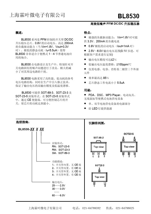
高效低噪声PFM DC/DC 升压稳压器BL8530概述:BL8530系列是PFM 控制的开关型DC/DC 升压稳压芯片。
0.8V 的启动电压、高达200mA的负载驱动能力(当Vin=1.8V ,Vout=3.3V 时),极低的静态功耗(I q <5.5uA )使得BL8530非常适合于便携式1~4节普通电池应用的场合。
BL8530在电路设计及生产中,特别针对开关电路固有的噪声问题进行了改良,极大的减小了对其周边电路的干扰。
BL8530电路采用了高性能、低功耗的参考电压电路结构,同时在生产中引入修正技术,保证了输出电压的高输出精度及低温度漂移。
BL8530可提供SOT-89-3、SOT-23-3及SOT-23-5封装形式。
在SOT-23-5封装形式中,通过CE 使能端,可方便控制芯片的开关,使芯片的功耗达到最小。
特点:• 极强的负载驱动能力: Vin=1.8V 时可提供3.3V 、200mA 的负载电流• 0.8V 极低的启动电压(Iout=1mA 时)• 2.5V ~6.0V 输出电压范围(0.1V 步进,可根据客户需求进行定制) • 输出电压精度可达±2%• 低输出电压温度漂移:±100ppm/℃• 仅需电感、电容、肖特基二极管三个外部元件• 效率最高达85%• 芯片静态工作电流小于5.5uA用途:• PDA 、DSC 、MP3 Player 、电动玩具、无线鼠标等便携式电池供电设备 • 单、双节电池供电设备的电源部分 •给LED 灯提供能源上海霖叶微电子有限公司 BL8530引脚定义表引脚号符号引脚描述SOT-89-3SOT-23-3 SOT-23-51 1 4 Vss(GND)接地引脚2 2 2 Vout输出电压监测,内部电路供电引脚3 3 5 Lx(Ext)开关引脚-- 3 NC 空脚-- 1 CE 使能端产品命名目录产品名称输出电压规格开关管 CE端封装形式V 内置无SOT-89-3BL8530-XX1SM XXBL8530-XX1RM XXV 内置无SOT-23-3V 内置有SOT-23-5BL8530-XX2RN XXBL8530-XX3SM XXV 外置无SOT-89-3BL8530-XX3RM XXV 外置无SOT-23-3BL8530-XX4RN XXV 外置有SOT-23-5系统框图:产品的极限参数输入电压------------------------------------------------------------------------------------------------0.3V~12VLx脚开关电压------------------------------------------------------------------------------------------0.3V~(Vout+0.3) CE脚电压-----------------------------------------------------------------------------------------------0.3V~(Vout+0.3) Lx脚输出电流-----------------------------------------------------------------------------------------0.7A允许的最大功耗,Pd T=25°CSOT-89-3------------------------------------------------------------------------------------------0. 5WSOT-23-5------------------------------------------------------------------------------------------0.15WSOT-23-3------------------------------------------------------------------------------------------0.15W最大工作结温-----------------------------------------------------------------------------------------150°C工作温度----------------------------------------------------------------------------------------------- -20~+80°C存贮温度----------------------------------------------------------------------------------------------- -40~125°C焊接温度和时间--------------------------------------------------------------------------------------260°C,10S推荐工作条件名称最小 推荐 最大 单位输入电压范围 0.8 Vout V 电感值10 27 100 µH 输入电容值 0 ≥10µF 输出电容值* 47 100 220 µF 工作环境温度 -20 85 ℃*:建议使用钽电容以减小输出电压的开关纹波。
5A输出可调线性稳压电源LM338

5A输出可调线性稳压电源LM338
田布荣
【期刊名称】《《电子制作》》
【年(卷),期】2005(000)011
【摘要】LM338是三端可调输出5A的线性稳压器。
主要特点:保证峰值电流输出7A;连续输出电流5A;输出电压范围1.2-32V;有电流输出限制;有输出短路保护;TO-220封装。
【总页数】1页(P35)
【作者】田布荣
【作者单位】
【正文语种】中文
【中图分类】TN248.22
【相关文献】
1.带输出短路保护和报警功能的直流可调稳压电源 [J], 陈淑芳
2.正负压可调的多路输出直流稳压电源设计 [J], 熊莹;罗云贵;张菊秀
3.一种输出可调智能开关稳压电源设计 [J], 周国雄;晏密英
4.1.2~57V/5A可调稳压电源 [J], 肖成定
5.基于LM2596的输出无级可调直流稳压电源的设计与实现 [J], 郑琪;刘琳;尚冬梅
因版权原因,仅展示原文概要,查看原文内容请购买。
- 1、下载文档前请自行甄别文档内容的完整性,平台不提供额外的编辑、内容补充、找答案等附加服务。
- 2、"仅部分预览"的文档,不可在线预览部分如存在完整性等问题,可反馈申请退款(可完整预览的文档不适用该条件!)。
- 3、如文档侵犯您的权益,请联系客服反馈,我们会尽快为您处理(人工客服工作时间:9:00-18:30)。
双输出低压美线性稳压器MAX8530
MAX8530是MAXIM公司生产的器件,它是一种双输出、低功耗、低压差线性稳压器。
该器件主要特点:输出1(OUT1)保证输出200mA;输出2(OUT2)保证输出150mA;OUT1及OUT2有多种电压输出(详见表1),用户也可根据电路需要确定要求的OUT1及OUT2的电压(在1.5~3.3V范围之内)向工厂订货;两个电源是相互独立的并且都是低压差,在100mA输出时其压差典型值为100mV;工作电压范围2.5~6.5V;当OUT1输出电压低于87%正常输出电压时,RESET端输出100ms的复位信号(低电平有效);静态电流小,典型值130μA;有省电关闭控制,关闭状态时耗电小于1μA;内部有输出电流限制,有过热及短路保护;有6焊球BGA及6管脚QFN两种封装;工作温度范围-40~+85℃。
管脚排列与功能
MAX8530的两种封装及管脚排列如图1所示,各管脚功能如表2所示。
QFN 封装用后缀EBT表示;UCSP封装用后缀ETT表示。
典型应用电路
MAX8530的典型应用电路如图2所示。
这是一个向基带μP供电的电路。
OUT1及OUT2的输出电压与型号的后缀有关,如表1所示。
输入电容器CIN取2.2μF,两个输出电容分别为2.2μF(OUT1)及1μF(OUT2),这三个电容器都采用贴片式多层陶瓷电容器。
MAX8530的RESET直接与基带μP 的RESET接口。
当OUT1的电压降到正常电压87%以下时,MAX8530的RESET 输出低电平,使基带μP复位。
上拉电阻可取10~100kΩ。
该器件组成的稳压器适用于手机及无绳电话、PDA、数码相机、PCMCIA卡及无线局域网卡等。