Reevaluating electron-phonon coupling strengths Indium as a test case for ab initio and man
英文原文
Liang Guo Stephen L.Hodson Timothy S.FisherXianfan Xu1e-mail:xxu@ School of Mechanical Engineering and Birck Nanotechnology Center,Purdue University,West Lafayette,IN47907Heat Transfer AcrossMetal-Dielectric Interfaces During Ultrafast-Laser Heating Heat transfer across metal-dielectric interfaces involves transport of electrons and pho-nons accomplished either by coupling between phonons in metal and dielectric or by cou-pling between electrons in metal and phonons in dielectric.In this work,we investigate heat transfer across metal-dielectric interfaces during ultrafast-laser heating of thin metalfilms coated on dielectric substrates.By employing ultrafast-laser heating that cre-ates strong thermal nonequilibrium between electrons and phonons in metal,it is possible to isolate the effect of the direct electron–phonon coupling across the interface and thus facilitate its study.Transient thermo-reflectance measurements using femtosecond laser pulses are performed on Au–Si samples while the simulation results based on a two-temperature model are compared with the measured data.A contact resistance between electrons in Au and phonons in Si represents the coupling strength of the direct electron–phonon interactions at the interface.Our results reveal that this contact resist-ance can be sufficiently small to indicate strong direct coupling between electrons in metal and phonons in dielectric.[DOI:10.1115/1.4005255]Keywords:interface thermal resistance,ultrafast laser,thermo-reflectance,two-temper-ature model,electron–phonon coupling1IntroductionInterface heat transfer is one of the major concerns in the design of microscale and nanoscale devices.In metal,electrons,and pho-nons are both energy carriers while in dielectric phonons are the main energy carrier.Therefore,for metal-dielectric composite structures,heat can transfer across the interface by coupling between phonons in metal and dielectric or by coupling between electrons in metal and phonons in dielectric through electron-interface scattering.Phonon–phonon coupling has been simulated mainly by the acoustic mismatch model and the diffuse mismatch model[1].As for electron–phonon coupling,there are different viewpoints.Some studies have assumed that electron–phonon coupling across a metal-dielectric interface is negligible and heat transfer occurs as electron–phonon coupling within metal and then phonon–phonon coupling across the interface[2].Electron–phonon coupling between metal(Cr,Ti,Al,Ni,and Pt)and SiO2 has exhibited negligible apparent thermal resistance using a parallel-strip technique[3].On the other hand,comparison between simulations and transient thermal reflectance(TTR) measurements for Au-dielectric interfaces reveals that energy could be lost to the substrate by electron-interface scattering dur-ing ultrafast-laser heating,and this effect depends on electron temperature and substrate thermal properties[4–6].In this study,we employ TTR techniques to investigate inter-face heat transfer for thin goldfilms of varying thicknesses on sili-con substrates.(Here,we consider silicon as a dielectric since heat is carried by phonons in silicon.)Similar work has been reported [5].In our model,we consider two temperatures in metal and also the temperature in the dielectric substrate.This allows us to inves-tigate the effect of both the coupling between electrons in metal and phonons in the dielectric substrate,and the coupling between phonons in metal and phonons in the dielectric substrate,and allows us to isolate the effect of the electron–phonon coupling across the interface that can be determined from the TTR mea-surement.Experimentally,we employ pulse stretching to mini-mize the effect of nonequilibrium among the electrons.As a result,the experimental data can be well-explained using the com-putational model.The thermal resistance between electrons in Au and phonons in Si,which quantifies the direct electron–phonon coupling strength,is calculated from the measured data.The results reveal that in the thermal nonequilibrium state,this electron–phonon coupling at the interface is strong enough to dominate the overall interface heat transfer.2TTR MeasurementAu–Si samples of varying Au thicknesses were prepared by thermal evaporation at a pressure of the order of10À7Torr.The thicknesses of the goldfilms are39,46,60,77,and250nm,meas-ured using an atomic force microscope.The pump-and-probe technique is used in a collinear scheme to measure the thermo-reflectance signal.The laser pulses are generated by a Spectra Physics Ti:Sapphire amplified femtosecond system with a central wavelength of800nm and a repetition rate of5kHz.The wave-length of the pump beam is then converted to400nm with a sec-ond harmonic crystal.The pump pulse has a pulse width(full width at half maximum-FWHM)of390fs measured by the sum-frequency cross-correlation method and is focused onto the sam-ple with a spot radius of20.3l m.The probe beam has a central wavelength of800nm and a pulse width of205fs measured by autocorrelation and is focused with a spot radius of16.9l m.This pump pulse width is intentionally stretched from the original pulse width of50fs to minimize the influence of thermal nonequili-brium among electrons since the electron thermalization time in Au can be of the order of100fs[7].This thermalization time is pump wavelength and pumpfluence dependent,and can be of the order of10fs if higher laserfluence is used[8,9].Our experiments did show the importance of pulse stretching.Figure1shows the TTR measurement results for the sample of thickness77nm with different pumpfluences before and after stretching the pulse.The plots show the normalized relative reflectance change(ÀD R/R)1Corresponding author.Contributed by the Heat Transfer Division of ASME for publication in the J OURNAL OF H EAT T RANSFER.Manuscript received May18,2011;final manuscript received September30,2011;published online February13,2012.Assoc.Editor: Robert D.Tzou.with the delay time between the pump and the probe pulses to show the contrast in cooling rates.With a shorter pulse (Fig.1(a )),a steep initial drop is seen in the signal,which is attributed to the behavior of nonequilibrium among electrons.Since the TTM to be used for simulation assumes a well-defined tempera-ture for electrons,i.e.,the electrons in gold have reached thermal equilibrium (not necessarily a uniform temperature),the model cannot predict the fast initial drop in the signals in Fig.1(a ).As will be shown later,the signals obtained by stretching the pulse can be predicted well using the TTM.3Two-Temperature Model for Thermal Reflectance MeasurementsUltrafast-laser heating induces thermal nonequilibrium between electrons and phonons in metal,which can be described by the TTM [10–13].We note that the heterogeneous interface consid-ered here involves three primary temperature variables (two in the metal and one in the dielectric).The “two-temperature”model is applied to the metal side.For investigating electron–phonon and phonon–phonon coupling at the interface,two thermal resistances are defined:R es (its reciprocal)indicates the coupling strength between electrons in metal and phonons in dielectric,while R ps indicates the coupling strength between phonons in metal and phonons in dielectric.(Large thermal resistance corresponds to weak coupling.)The resulting governing equations,initial,and interface conditions areC e @T e @t ¼k e @2T e@x2ÀG ðT e ÀT p ÞþS (1a )C p @T p @t ¼k p @2T p @x 2þG ðT e ÀT p Þ(1b )C s @T s @t ¼k s @2T s@x(1c )T e ðt ¼0Þ¼T p ðt ¼0Þ¼T s ðt ¼0Þ¼T 0(2)Àk e@T e @xx ¼L ¼T e ÀT s R es x ¼L(3a )Àk p @T px ¼L ¼T p ÀT s ps x ¼L(3b )Àk s@T sx ¼L ¼T e ÀT s es x ¼L þT p ÀT s ps x ¼L(3c )The subscripts e ,p ,and s denote electrons in metal,phonons in metal,and phonons in the dielectric substrate,respectively.C is the volumetric heat capacity,k is the thermal conductivity,G is the electron–phonon coupling factor governing the rate of energy transfer from electrons to phonons in metal,and L is the thickness of the metal layer.At the front surface of the metal layer insula-tion boundary condition is used due to the much larger heat flux caused by laser heating relative to the heat loss to air.At the rear surface of the substrate,since the thickness of the substrate used is large enough (1l m)so that there is no temperature rise during the time period of consideration,the insulation boundary condition is also applied.Thermal properties of phonons in both metal and dielectric are taken as temperature-independent due to the weak temperature dependence.The thermal conductivity of phonons in metal is much smaller than that of the electrons and is taken in this work as 0.001times the bulk thermal conductivity of gold (311W/(mK)).The volumetric heat capacity of the metal phonon is taken as that of the bulk gold.C e is taken as proportional to T e [14]with the proportion coefficient being 70J/(m 3K 2)[15],and k e is calculated by the model and the data used in Ref.[13]which is valid from the room temperature to the Fermi temperature (6.39Â104K in Au,[14]).G can be obtained using the model derived in Ref.[16].In this work,the value of G at the room tem-perature is taken as 4.6Â1016W/(m 3K)[17],and its dependence on electron and phonon temperatures follows [16].The laser heat-ing source term S is represented by the model used in [13]asS ¼0:94ð1ÀR ÞJ t p ðd þd b Þ1Àexp ÀL d þd bexp Àx d þd b À2:77t t p2"#(4)which assumes all the absorbed laser energy is deposited in the metal layer.J is the fluence of the pump laser,R is the surface re-flectance to the pump,t p is the pulse width (FWHM),d is the opti-cal penetration depth,and d b is the electron ballistic length (around 100nm in Au,[18]).R es and R ps are treated as free pa-rameters for fitting the experimental data.The wavelength of the probe laser in the experiment is centered at 800nm.For this wavelength,the incident photon energy is below the interband transition threshold in Au,which is around 2.47eV [18],and the Drude model can be used to relate the tem-peratures of electrons and phonons to the dielectric function and then the index of refraction,which is expressed as [19]e ¼e 1Àx 2px ðx þi x s Þ(5)x is the frequency of the probe laser and x p is the plasma fre-quency (1.37Â1016rad/s in Au evaluated using the data in Ref.[14]).x s is the electron collisional frequency,the inverse of the electron relaxation time.The temperature dependence ofelectricalFig.1TTR measurement results for the Au–Si sample of Authickness 77nm with different fluences.(a )Results before pulse stretching;(b )results after pulse stretching.resistivity indicates that x s is approximately proportional to pho-non temperature at high temperature [14]and from the Fermi liq-uid theory,its variation with electron temperature is quadratic (T e 2)[20].Therefore,x s is related to T e and T p approximately asx s ¼A ee T 2e þB ep T p(6)A ee is estimated from the low-temperature measurement [21]andB ep is usually estimated from the thermal or electrical resistivity near the room temperature [14].In this work,A ee is taken as the lit-erature value 1.2Â107s À1K À2[6]while e 1and B ep are evaluated by fitting the room-temperature value of the complex dielectric con-stant at 800nm wavelength provided in Ref.[22],which are found to be 9.7and 3.6Â1011s À1K À1,respectively.The complex index of refraction n 0þin 00is the square root of the dielectric ing Eqs.(5)and (6),n 0and n 00are evaluated as 0.16and 4.90,respectively,which agree with the empirical values [23].The re-flectance is then calculated from n 0and n 00by the method of transfer matrix [24],which considers multiple reflections in thin films.4Results and DiscussionThe results of TTR measurements with a pump fluence of 147J/m 2are plotted in Fig.2.The fast decrease of the reflectance indicates that energy transfer between electrons and phonons in metal,followed by a relatively slow decrease after several ps which indicates electrons and phonons have reached thermal equi-librium.The initial cooling rates are smaller for samples with thicknesses less than the electron ballistic length since the electron temperature is almost uniform across the thin film,and coupling with phonons within the metal film and the dielectric substrate is the only cooling mechanism.For a thicker sample of thickness 250nm,the initial decrease is much faster due to thermal diffu-sion in the gold film caused by a gradient of the electron tempera-ture in the film.We investigate the effect of R es and R ps using the thermo-reflectance signal.Two values of R ps ,1Â10À10m 2K/W and 1Â10À7m 2K/W,are used,each with a parameterized range of values for R es .Figure 3shows the calculated results for the sample with a 39nm-thick gold film.Little difference can be seen between Figs.3(a )and 3(b )while different cooling rates are obtained with varying R es in either plot,indicating that the cooling rate is not sensitive to the coupling strength between phonons in metal and dielectric.Note that an interface resistance of 1Â10À10m 2K/W is lower than any reported value,indicating a very high coupling strength between the phonons in metal and dielectric.Conversely,the results vary greatly with the coupling strength between electrons in metal and phonons in dielectric at the interface.This is because the lattice (phonon)temperature rise in metal is much smaller than the elec-tron temperature that the interface coupling between phonons in metal and dielectric does not influence the surface temperature,which directly determines the measured reflectance.On the other hand,the temperature rise of electrons is much higher,and conse-quently,the cooling rate is sensitive to R es .The relatively high sensitivity of R es to that of R ps demonstrates that the former can be isolated for the study of the coupling between electrons in metal and phonons in dielectric.We now use the measured TTR data to estimate R es ,the thermal resistance between electrons in metal and phonons in dielectric.R es is adjusted by the least square method to fit the simulation results with the measured data,and the results are shown in Fig.4.We note that it is impossible to fit the measured results using insu-lation interface condition (i.e.,no coupling or extremely large thermal resistance between electrons in metal and phonons in the dielectric substrate),which will significantly underestimate the cooling rate.For thin samples,we find that the value of R es is of the order of 10À10to 10À9m 2K/W.This value is below the ther-mal resistances of representative solid–solid interfaces measured in thermal equilibrium [25].This indicates that the direct coupling between electrons in metal and phonons in dielectric is strong.It is also noted that the resistance values increases with the thickness of the gold film,indicating a decrease in the coupling strength between electrons in metal and the dielectric substrate.This could be due to the lower electron temperature obtained in thicker films,and a decrease of the coupling strength with a decrease in the electron temperature [5].For the sample of thickness 250nm,R es has little effect on the simulation result since the interface is too far from the absorbing surface to influence the surface tempera-ture,and therefore it is not presented here.The agreement between the fitted results and the measured data is generally good.The small discrepancy between the measured and the fitted results can result from inaccuracy in computingtheFig.2TTR measurement results on Au–Si samples of varying AuthicknessesFig.3Simulation results with varying R es for the Au–Si sample of Au thickness 39nm.(a )R ps 51310210m 2K/W;(b )R ps 5131027m 2K/W.absorption or the temperature.Figure 1(b)shows the normalized TTR measurement results on the sample of thickness 77nm with three laser fluences.It is seen that small variations in the shape of the TTR signals can be caused by different laser fluences and thus the maximum temperature reached in the film.Absorption in metal,multiple reflections between the metal surface and the Au–Si inter-face,and possible deviations of the properties of thin films from those of bulk can all contribute to uncertainties in the temperature simulation;therefore affecting the calculated reflectance.With the values of R es shown in Fig.4,the calculation shows that the highest electron temperature,which is at the surface of 39nm–thick gold film,is about 6700K.The highest temperature of electrons is roughly inversely proportional to the thickness of the films for the four thinner films.The highest temperature of elec-trons is much less than the Fermi temperature and thus ensures the validity of the linear dependence of C e on T e [14].The highest temperature for the lattice in metal is about 780K,also in the 39nm-thick gold film.This large temperature difference between electrons and lattice indicates that the interface heat transfer is dominated by the coupling between electrons in metal and the phonons in the dielectric substrate.As shown in Fig.4,the meas-ured R es is very low,of the order of 10À10to 10À9m 2K/W.Even if R ps ,which is not determined in this study,is also that low (note that 10À10to 10À9m 2K/W is lower than any reported values),because of the large difference in temperatures between electrons and the phonons in metal,the interface heat transfer rate (Eqs.(3a )–(3c ))due to the coupling between electrons in metal and the substrate is much larger than that due to the coupling between phonons in metal and the substrate.5ConclusionsIn conclusion,TTR measurements using femtosecond laser pulses are performed on Au–Si samples and the results are analyzed using the TTM model.It is shown that due to the strong nonequilibrium between electrons and phonons during ultrafast-laser heating,it is possible to isolate the effect of the direct electron–phonon coupling across the interface,allowing investiga-tion of its ing stretched femtosecond pulses is shown to be able to minimize the nonequilibrium effect among electrons,and is thus more suitable for this study.The TTR measurement data can be well-represented using the TTM parison between the TTR data and the TTM results indicates that the direct coupling due to electron-interface scattering dominates the interface heat transfer during ultrafast-laser heating of thin films.AcknowledgmentThis paper is based upon work supported by the Defense Advanced Research Projects Agency and SPAWAR Systems Cen-ter,Pacific under Contract No.N66001-09-C-2013.The authors also thank C.Liebig,Y.Wang,and W.Wu for helpful discussions.NomenclatureA ee ¼coefficient in Eq.(6),s À1K À2B ep ¼coefficient in Eq.(6),s À1K À1C ¼volumetric heat capacity,J/(m 3K)G ¼electron–phonon coupling factor,W/(m 3K)i ¼unit of the imaginary number J ¼fluence of the pump,J/m 2k ¼thermal conductivity,W/(mK)L ¼metal film thickness,mn 0¼real part of the complex index of refractionn 00¼imaginary part of the complex index of refraction R ¼interface thermal resistance,m 2K/W;reflectance S ¼laser source term,W/m3Fig.4Comparison between the measurement and the simulation results for Au–Si samples of different Au thicknesses.The open circle represents the meas-ured data and the solid line represents the simulation results.(a )39nm fitted by R es 55310210m 2K/W;(b )46nm fitted by R es 56310210m 2K/W;(c )60nm fitted by R es 51.231029m 2K/W;and (d )77nm fitted by R es 51.831029m 2K/W.T¼temperature,Kt¼time,st p¼pulse width of the pump(FWHM),sx¼spatial coordinate,me¼complex dielectric constante1¼constant in the Drude modeld¼radiation penetration depth,md b¼electron ballistic depth,mx¼angular frequency of the probe,rad/sx p¼plasma frequency,rad/sx s¼electron collisional frequency,rad/sSubscripts0¼initial statee¼electron in metales¼electron in metal and phonon in dielectricp¼phonon in metalps¼phonon in metal and phonon in dielectrics¼phonon in dielectricReferences[1]Cahill,D.G.,Ford,W.K.,Goodson,K.E.,Mahan,G.D.,Majumdar,A.,Maris,H.J.,Merlin,R.,and Phillpot,S.R.,2003,“Nanoscale Thermal Trans-port,”J.Appl.Phys.,93(2),pp.793–818.[2]Majumdar,A.,and Reddy,P.,2004,“Role of Electron–Phonon Coupling inThermal Conductance of Metal–Nonmetal Interfaces,”Appl.Phys.Lett., 84(23),pp.4768–4770.[3]Chien,H.-C.,Yao,D.-J.,and Hsu,C.-T.,2008,“Measurement and Evaluationof the Interfacial Thermal Resistance Between a Metal and a Dielectric,”Appl.Phys.Lett.,93(23),p.231910.[4]Hopkins,P.E.,and Norris,P.M.,2007,“Substrate Influence in Electron–Phonon Coupling Measurements in Thin Au Films,”Appl.Surf.Sci.,253(15), pp.6289–6294.[5]Hopkins,P.E.,Kassebaum,J.L.,and Norris,P.M.,2009,“Effects of ElectronScattering at Metal–Nonmetal Interfaces on Electron-Phonon Equilibration in Gold Films,”J.Appl.Phys.,105(2),p.023710.[6]Hopkins,P.E.,2010,“Influence of Electron-Boundary Scattering on Thermore-flectance Calculations After Intraband and Interband Transitions Induced by Short-Pulsed Laser Absorption,”Phys.Rev.B,81(3),p.035413.[7]Sun,C.-K.,Vallee,F.,Acioli,L.,Ippen,E.P.,and Fujimoto,J.G.,1993,“Femtosecond Investigation of Electron Thermalization in Gold,”Phys.Rev.B, 48(16),pp.12365–12368.[8]Fann,W.S.,Storz,R.,Tom,H.W.K.,and Bokor,J.,1992,“Electron Thermal-ization of Gold,”Phys.Rev.B,46(20),pp.13592–13595.[9]Fann,W.S.,Storz,R.,Tom,H.W.K.,and Bokor,J.,1992,“Direct Measure-ment of Nonequilibrium Electron-Energy Distributions in Subpicosecond Laser-Heated Gold Films,”Phys.Rev.Lett.,68(18),pp.2834–2837.[10]Kaganov,M.I.,Lifshitz,I.M.,and Tanatarov,L.V.,1957,“RelaxationBetween Electrons and the Crystalline Lattice,”Sov.Phys.JETP,4(2),pp.173–178.[11]Anisimov.S.I.,Kapeliovich,B.L.,and Perel’man,T.L.,1974,“ElectronEmission From Metal Surfaces Exposed to Ultrashort Laser Pulses,”Sov.Phys.JETP,39(2),pp.375–377.[12]Qiu,T.Q.,and Tien,C.L.,1993,“Heat Transfer Mechanisms During Short-Pulse Laser Heating of Metals,”ASME Trans.J.Heat Transfer,115(4),pp.835–841.[13]Chowdhury,I.H.,and Xu,X.,2003,“Heat Transfer in Femtosecond LaserProcessing of Metal,”Numer.Heat Transfer,Part A,44(3),pp.219–232. [14]Kittel,C.,1976,Introduction to Solid State Physics,John Wiley&Sons,Inc.,New York.[15]Smith,A.N.,and Norris,P.M.,2001,“Influence of Intraband Transitions onthe Electron Thermoreflectance Response of Metals,”Appl.Phys.Lett.,78(9), pp.1240–1242.[16]Chen,J.K.,Latham,W.P.,and Beraun,J.E.,2005,“The Role of Electron–Phonon Coupling in Ultrafast Laser Heating,”ser Appl.,17(1),pp.63–68.[17]Hostetler,J.L.,Smith,A.N.,Czajkowsky,D.M.,and Norris,P.M.,1999,“Measurement of the Electron-Phonon Coupling Factor Dependence on Film Thickness and Grain Size in Au,Cr,and Al,”Applied Optics,38(16),pp.3614–3620.[18]Hohlfeld,J.,Wellershoff,S.-S.,Gudde,J.,Conrad,U.,Jahnke,V.,and Mat-thias,E.,2000,“Electron and Lattice Dynamics Following Optical Excitation of Metals,”Chem.Phys.,251(1–3),pp.237–258.[19]Maier,S.A.,2007,Plasmonics:Fundamentals and Applications,SpringerScienceþBusiness Media,New York.[20]Ashcroft,N.W.,and Mermin,N.D.,(1976),Solid State Physics,W.B.Saun-ders,Philadelphia.[21]MacDonald,A.H.,1980,“Electron-Phonon Enhancement of Electron-ElectronScattering in Al,”Phys.Rev.Lett.,44(7),pp.489–493.[22]Johnson,P.B.,and Christy,R.W.,1972,“Optical Constants of the Noble Met-als,”Phys.Rev.B,6(12),pp.4370–4379.[23]Palik,E.D.,(1998),Handbook of Optical Constants of Solids,Academic,SanDiego.[24]Pedrotti,F.L.,Pedrotti,L.S.,and Pedrotti,L.M.,(2007),Introduction toOptics,Pearson Prentice Hall,Upper Saddle River,NJ.[25]Incropera,F.P.,Dewitt,D.P.,Bergman,T.L.,and Lavine,A.S.,2007,Funda-mentals of Heat and Mass Transfer,John Wiley&Sons,Inc.,Hoboken,NJ.。
二甲基噻吩骨架三齿膦配体、其合成方法、其铜配合物及其铜配合物

专利名称:二甲基噻吩骨架三齿膦配体、其合成方法、其铜配合物及其铜配合物的合成方法和应用
专利类型:发明专利
发明人:柳利,魏琼
申请号:CN201910552283.3
申请日:20190625
公开号:CN110272453A
公开日:
20190924
专利内容由知识产权出版社提供
摘要:本发明属于铜配合物技术领域,具体涉及一种基于二甲基噻吩骨架的三齿膦配体、其合成方法、其铜配合物及其铜配合物的合成方法和应用。
本发明所提供的基于二甲基噻吩骨架的三齿膦配体的单核四配位卤化亚铜配合物可发强烈的黄绿光,热分解温度高,热稳定高,适合作为OLED发光材料。
申请人:湖北大学
地址:430062 湖北省武汉市武昌区友谊大道368号
国籍:CN
代理机构:北京轻创知识产权代理有限公司
代理人:冯瑛琪
更多信息请下载全文后查看。
具有改良溶出速度的达芦那韦组合物的制作方法
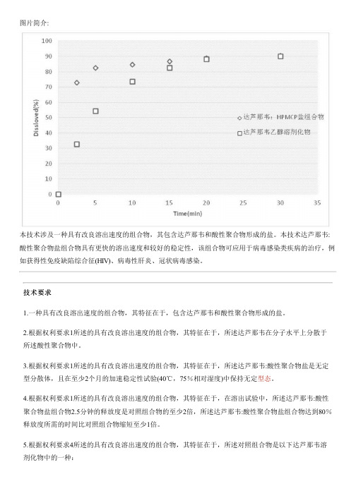
图片简介:本技术涉及一种具有改良溶出速度的组合物,其包含达芦那韦和酸性聚合物形成的盐。
本技术达芦那韦:酸性聚合物盐组合物具有更快的溶出速度和较好的稳定性,该组合物可应用于病毒感染类疾病的治疗,例如获得性免疫缺陷综合征(HIV)、病毒性肝炎、冠状病毒感染。
技术要求1.一种具有改良溶出速度的组合物,其特征在于,包含达芦那韦和酸性聚合物形成的盐。
2.根据权利要求1所述的具有改良溶出速度的组合物,其特征在于,所述达芦那韦在分子水平上分散于所述酸性聚合物中。
3.根据权利要求1所述的具有改良溶出速度的组合物,其特征在于,所述达芦那韦:酸性聚合物盐是无定型分散体,且在至少2个月的加速稳定性试验(40℃,75%相对湿度)中保持无定型态。
4.根据权利要求1所述的具有改良溶出速度的组合物,其特征在于,在溶出试验中,所述达芦那韦:酸性聚合物盐组合物2.5分钟的释放度是对照组合物的至少2倍,所述达芦那韦:酸性聚合物盐组合物达到80%释放度所需的时间比对照组合物缩短至少1倍。
5.根据权利要求4所述的具有改良溶出速度的组合物,其特征在于,所述对照组合物是以下达芦那韦溶剂化物中的一种:达芦那韦乙醇溶剂化物、达芦那韦水合物、达芦那韦甲醇溶剂化物、达芦那韦丙酮溶剂化物、达芦那韦二氯甲烷溶剂化物、达芦那韦乙酸乙酯溶剂化物、达芦那韦1-乙氧基-2-丙醇溶剂化物、达芦那韦苯甲醚溶剂化物、达芦那韦四氢呋喃溶剂化物、达芦那韦异丙醇溶剂化物、达芦那韦甲磺酸溶剂化物。
6.根据权利要求1所述的具有改良溶出速度的组合物,其特征在于,所述达芦那韦:酸性聚合物盐组合物为口服剂型。
7.根据权利要求1所述的具有改良溶出速度的组合物,其特征在于,所述达芦那韦:酸性聚合物盐组合物包含达芦那韦:酸性聚合物的重量比为20:1至1:20,或,所述达芦那韦:酸性聚合物盐组合物包含达芦那韦:酸性聚合物的重量比为10:1至1:10。
8.根据权利要求1所述的具有改良溶出速度的组合物,其特征在于,单剂量中包含酸性聚合物的重量范围为1mg至10g、20mg至1g、20mg至400mg中的一种;单剂量中包含达芦那韦的重量范围为1mg至800mg、20mg至600mg、1mg至200mg、1mg至100mg、1mg至30mg中的一种。
偕胺肟基化合物的合成及表征

偕胺肟基化合物的合成及表征
本文将对偕胺肟基化合物的合成及表征进行介绍。
偕胺肟基化合物是指具有活性偶氮结构的有机化合物,它们以N-N异构体形式
存在,常备受到医药科学、农药以及苯氧类衍生物的研究和应用。
由于其具有稳定性好,围绕C=N这一共价键合成活性元素组合是一类重要的化学反应,在有机合成中发挥着重要作用。
偕胺肟基化合物的合成有两种方法,一种是通过氢化反应,另一种是通过格氏
外电子环扩散(Grignard reaction)。
在氢化反应中,胺肟会经历还原和氢化机理,它们可以与受氢作用后的羰基相互反应,形成氯化物通过水解还原到直键异构体。
在Grignard reaction中,Grignard试剂可以与胺肟的直接碱水合物发生反应,生成活性偶氮结构,从而获得偕胺肟类化合物。
偕胺肟基化合物表征主要有正核磁共振(NMR)、质谱(mass spectrometry)、X射线衍射(XRD)和电子探针(EPT)等等,其中NMR是用来鉴定一种化合物的杂
化性质,而mass spectrometry可以识别出分子中的元素和分子,从而辨识化合物的结构,同样XRD可以用来判断分子同位异构体的存在,而电子探针可判断不同位置原子间的位置关系。
综上所述,偕胺肟基化合物的合成及表征在医药科学、农药以及苯氧类衍生物
的研究中发挥着重要作用,获得偕胺肟类化合物可以通过氢化反应或格氏外电子环扩散来实现,而用于偕胺肟类化合物表征的主要方法是NMR、mass spectrometry、XRD和EPT。
从微藻中提取β-烟酰胺单核苷酸的方法及微藻提取物

从微藻中提取β-烟酰胺单核苷酸的方法及微藻提取物下载提示:该文档是本店铺精心编制而成的,希望大家下载后,能够帮助大家解决实际问题。
文档下载后可定制修改,请根据实际需要进行调整和使用,谢谢!本店铺为大家提供各种类型的实用资料,如教育随笔、日记赏析、句子摘抄、古诗大全、经典美文、话题作文、工作总结、词语解析、文案摘录、其他资料等等,想了解不同资料格式和写法,敬请关注!Download tips: This document is carefully compiled by this editor. I hope that after you download it, it can help you solve practical problems. The document can be customized and modified after downloading, please adjust and use it according to actual needs, thank you! In addition, this shop provides you with various types of practical materials, such as educational essays, diary appreciation, sentence excerpts, ancient poems, classic articles, topic composition, work summary, word parsing, copy excerpts, other materials and so on, want to know different data formats and writing methods, please pay attention!从微藻中提取β烟酰胺单核苷酸的方法及微藻提取物1. 引言在当今社会,人们对健康和美容的关注度越来越高。
双极性反式类胡萝卜素盐及其应用[发明专利]
![双极性反式类胡萝卜素盐及其应用[发明专利]](https://img.taocdn.com/s3/m/338e6d3749649b6648d747f6.png)
专利名称:双极性反式类胡萝卜素盐及其应用专利类型:发明专利
发明人:约翰·L·盖纳,雷蒙德·C·格拉别克
申请号:CN03804566.4
申请日:20030225
公开号:CN1671643A
公开日:
20050921
专利内容由知识产权出版社提供
摘要:本发明涉及双极性反式类胡萝卜素盐化合物、该类化合物的增溶方法、合成方法以及使用方法。
这类化合物可用于改善氧在包括人类在内的哺乳动物的血红细胞和机体组织之间的扩散能力。
申请人:扩散药品有限公司
地址:美国弗吉尼亚州
国籍:US
代理机构:北京三友知识产权代理有限公司
代理人:丁香兰
更多信息请下载全文后查看。
聚鲁米诺修饰复合电极电化学发光分析法测定豆类样品中钼(Ⅵ)含量

徐艺凤,徐承娥,熊海涛. 聚鲁米诺修饰复合电极电化学发光分析法测定豆类样品中钼(Ⅵ)含量[J]. 食品工业科技,2024,45(5):205−211. doi: 10.13386/j.issn1002-0306.2023030272XU Yifeng, XU Cheng’e, XIONG Haitao. Electrochemiluminescence Determination of Mo(Ⅵ) Content in Beans Based on Polyluminol Composite Modified Electrode[J]. Science and Technology of Food Industry, 2024, 45(5): 205−211. (in Chinese with English abstract). doi: 10.13386/j.issn1002-0306.2023030272· 分析检测 ·聚鲁米诺修饰复合电极电化学发光分析法测定豆类样品中钼(Ⅵ)含量徐艺凤,徐承娥,熊海涛*(陕西理工大学化学与环境科学学院,陕西汉中 723001)摘 要:本研究基于Mo (Ⅵ)对鲁米诺电还原发光信号的增敏作用,结合石墨烯与带正电荷的纳米金((+)AuNPs )的电信号放大作用,建立了一种灵敏且准确检测豆类种子中Mo (Ⅵ)含量的电化学发光新方法。
采用滴涂法先将Nafion-石墨烯修饰于玻碳电极表面,再通过静电组装及电化学聚合技术依次将(+)AuNPs 、鲁米诺修饰于电极表面,从而制得Nafion-石墨烯/(+)AuNPs/聚鲁米诺复合修饰电极。
通过循环伏安法与电化学发光技术对复合修饰电极进行了初步表征,并对测定Mo (Ⅵ)的实验条件进行了优化。
结果表明,在饱和硼砂缓冲溶液、电位扫描速率100 mV/s 、富集时间13 min 等优化实验条件下,Mo (Ⅵ)浓度在5.0×10⁻⁹~1.0×10⁻⁶ mol/L 范围内与复合修饰电极表面增敏的电还原发光信号呈现良好的线性关系,检出限(3σ)与相对标准偏差分别为2.1×10⁻⁹mol/L 及2.4%(C=1.0×10⁻⁷ mol/L ,n=11)。
槲皮素分子印迹聚邻苯二胺敏感膜电化学传感器
槲皮素分子印迹聚邻苯二胺敏感膜电化学传感器王微;孙红;赫春香【摘要】以槲皮素为模板分子,邻苯二胺为功能单体,采用循环伏安法制备了槲皮素分子印迹薄膜修饰电极,并将其用于槲皮素的检测.在HAc-NH4Ac缓冲溶液(pH 4.0)中,以微分脉冲伏安法为电化学激发信号,槲皮素在0.37 V(VS.SCE)处产生一个灵敏的氧化峰,峰电流与其浓度在8.00×10⁻⁸~1.00×10⁻³ mol/L 范围内呈线性关系,实验检出限为5.00×10⁻⁸ mol/L.将新方法应用于2种银杏叶类药物中槲皮素的测定,回收率在99.2%~102%之间.【期刊名称】《高师理科学刊》【年(卷),期】2012(000)006【总页数】3页(P50-52)【关键词】槲皮素;邻苯二胺;分子印迹膜;微分脉冲伏安法【作者】王微;孙红;赫春香【作者单位】辽宁师范大学化学化工学院,辽宁大连 116029;辽宁师范大学化学化工学院,辽宁大连 116029;辽宁师范大学化学化工学院,辽宁大连 116029【正文语种】中文【中图分类】O657.1槲皮素(Quercetin,Qu)具有多种药用价值,因而在黄酮类化合物中占有重要的地位[1],其测定方法的研究在鉴定生产原料品质、评价生物制剂工艺以及药代动力学分析等方面具有重要意义.目前,检测槲皮素的方法主要有毛细管电泳法[2]、高效液相色谱法[3]、荧光法[4]和电化学检测方法[5-7].将分子印迹技术应用于传感器的研制是近年来出现的新技术[8].邻苯二胺(o-pheny-lenediamine,OPD)是制备分子印迹电化学传感器常用的功能单体,采用电化学方法可以直接在基体电极表面聚合成带有模板印迹的聚合物[9].这种分子印迹技术不需要交联剂和致孔剂,具有简便、快速的优点.本文以槲皮素为模板分子,邻苯二胺为功能单体,制备了槲皮素分子印迹电化学传感器,并建立了微分脉冲伏安法测定槲皮素的新方法.本方法具有灵敏度高、选择性好、方法简便等优点.LK9805电化学分析仪(天津市兰力科电子科技发展有限公司);三电极系统:以石墨(SG)、聚邻苯二胺/石墨、槲皮素/邻苯二胺/石墨分子印迹修饰电极为工作电极,饱和甘汞电极为参比电极(文中全部电位均相对于饱和甘汞电极),铂丝电极为辅助电极.槲皮素、芦丁、桑色素、葛根素和山奈酚(由西安天本生物工程有限公司提供,纯度>98%).除指明外其它化学试剂均为分析纯.实验用水为石英亚沸二次蒸馏水. 1.2.1 分子印迹修饰电极的制备将光谱纯石墨棒制成蜡浸石墨电极(SG),并清洗至洁净[10].以SG为工作电极,含有1.00×10⁻² mol/L OPD,4.00×10-4mol/L Qu,0.10 mol/L KCl的混合溶液为修饰剂,在+1.50 ~-1.00 V电位范围内,以0.05 V/s的扫速连续循环伏安扫描30圈.取出电极,用水冲洗,再置于pH 7.0 的磷酸盐缓冲溶液(PBS)中,循环扫描30圈,得到具有槲皮素印迹的聚邻苯二胺石墨修饰电极(MIPCME).不加入模板分子(槲皮素)制备非分子印迹修饰电极(NIPCME).1.2.2 槲皮素的测定以MIPCME为工作电极,静置吸附300 s,-0.30 V为起点电位,在-0.30~0.60 V电位范围内记录微分脉冲伏安曲线,根据 0.37 V 处的峰电流进行定量分析.分别以SG,NIPCME,MIPCME为工作电极,测定5 mmol/L K3Fe(CN)6(0.1 mol/L KNO3中)的循环伏安曲线(见图1).结果表明,K3Fe(CN)6在NIPCME电极上没有电化学响应,在MIPCME上出现氧化还原峰,但是峰电流明显小于其在SG电极上的响应.说明NIPCME是电惰性的,而MIPCME上存在空穴.分别以SG,MIPCME,NIPCME为工作电极,按照实验方法测定5.00×10⁻⁵ mol/L槲皮素.结果表明,槲皮素在MIPCME上的峰电流远远大于在SG电极上电流响应(见图2).分别试验了槲皮素在HAc-NH4Ac(pH 4.00~6.00 ),NH3-NH4Cl(pH8.00~10.00),PBS(pH 4.00~10.00)中的电化学响应.结果表明,以pH 4.0 的HAc -NH4Ac缓冲溶液作为支持电解质时峰电流最大.实验发现,吸附时间对峰电流有明显的影响,最佳吸附时间为300 s.在8.00×10⁻⁸~1.00×10⁻³mol/L范围内,槲皮素的浓度与峰电流呈线性关系,回归方程ip(μA)= 3.14 c(μmol/L)+ 4.33(r=0.998),实验检出限5.00×10⁻⁸ mol/L.一支电极平行测定6组同浓度的槲皮素,响应值的相对标准偏差(RSD)为1.2 %;平行制备4支电极,RSD为3.3 %.在允许存在10 % 误差的前提下,桑色素、葛根素和山奈酚不干扰测定.芦丁对本方法有一定的干扰,最大共存量为槲皮素的60倍.此外,实验还表明,测定体系中允许共存300倍的十二烷基磺酸钠,150倍的抗坏血酸,100倍的聚乙烯醇,50倍的草酸和柠檬酸钠.其它常见金属离子均不干扰测定.测定了舒血宁注射液(1#)和银杏叶分散片(2#)中槲皮素的质量分数.银杏叶中黄酮苷的代表成分是槲皮苷、山萘酚苷、芦丁苷和鼠李糖苷[11].据此对药品进行预处理:将试样溶液与 50 mL 0.5 % 的硫酸和45 mL无水乙醇混合,加热回流1 h,冷却,用无水乙醇定容至100 mL.处理后槲皮苷转化成槲皮素,芦丁水解转化成槲皮素,结果见表1,平均回收率(n=3)分别为99.2%,102%.表明此方法适用于实际样品中槲皮素的测定.【相关文献】[1] Luo Yiping.Advances in Pharmacological Research of Flavonoids[J].Asia-Pacific Traditional Medicine,2010(4):132-134[2] Dadakova E,Kalinova J.Determination of quercetin glycosides and free quercetin in buckwheat by capillary micellar electrokimetic chromatography[J].Journal of Separation Science,2010,33:1633-1638[3] Du FY,Xiao XH.Lonic lipquid aqueous solvent-based microwave-assisted hydrolysis for the extraction and HPLC determination of myricetin and quercetin from Myrica rubra leaves[J].Biomedical Chromatography,2011,25:472-478[4] Chen Daiwu,Xie Qingji.Fluorescent Studies on the Interactions of Quercetin with Aminoacid[J].Chemical Research,2009(4):78- 81[5] 轩卫华,曹红,龚晓武,等.槲皮素在悬汞电极上的伏安行为研究[J].分析试验室,2011,29(11):32-35[6] Ziyatdinova G,Aytuganova I,Nizamova A,et al.Cyclic voltammetry of natural flavonoids mwnt-modified electrode and their determination inpharmaceuticals[J].Collection of Czechoslovak chemical communications,2011,76:1619-1631[7] 王明艳,许兴友,马卫兴,等.4-(3-吡啶基)-2-巯基咪唑修饰金电极一阶微分线性扫描伏安法直接测定复方鱼腥草片中槲皮素[J].理化检验:化学分册,2010,46(10):1125-1128,1131[8] 朱玲艳,王宗花,陈小印,等.聚吡咯/碳纳米管分子印迹修饰电极对槲皮素的选择性测定[J].分析测试学报,2011,30(1):18-23[9] Tanji Y, Wanzhi W,Jinxiang Z. Selective detection of dopamine in the presence of ascorbic acid by use of glassy-carbon electrodes modified with both polyaniline film and multi-walled carbon nanotubes with incorporated β-cyclodextrin[J].Analytical and Bioanalytical Chemistry,2006,386:2087-2094[10] 李晓娟,赫春香.铁氰化镍/银复合修饰电极的制备及对氟康唑的电吸附作用[J].高师理科学刊,2009,29(1):68-71[11] 唐于平,王颖,楼凤昌,等.银杏叶中的黄酮醇苷类成分[J].药学学报,2000,35(5):363-366。
- 1、下载文档前请自行甄别文档内容的完整性,平台不提供额外的编辑、内容补充、找答案等附加服务。
- 2、"仅部分预览"的文档,不可在线预览部分如存在完整性等问题,可反馈申请退款(可完整预览的文档不适用该条件!)。
- 3、如文档侵犯您的权益,请联系客服反馈,我们会尽快为您处理(人工客服工作时间:9:00-18:30)。
a rX iv:c ond-ma t/98653v1[c ond-m at.s upr-con]3J un1998Reevaluating electron–phonon coupling strengths:Indium as a test case for ab initio and many-body–theory methods Sven P.Rudin †,R.Bauer,‡Amy Y.Liu,†and J.K.Freericks ††Department of Physics,Georgetown University,Washington,D.C.20057-0995,U.S.A.‡Theoretische Physik,Universit¨a t Regensburg,D-93040Regensburg,Germany Abstract Using indium as a test case,we investigate the accuracy of the electron–phonon coupling calculated with state-of-the-art ab initio and many-body theory methods.The ab initio calculations —where electrons are treated in the local-density approximation,and phonons and the electron–phonon in-teraction are treated within linear response —predict an electron–phonon spectral function α2F (ω)which translates into a relative tunneling conduc-tance that agrees with experiment to within one part in 103.The many-body theory calculations —where α2F (ω)is extracted from tunneling data by means of the McMillan-Rowell tunneling inversion method —provide spec-tral functions that depend strongly on details of the inversion process.For the the most important moment of α2F (ω),the mass-renormalization parameter λ,we report 0.9±0.1,in contrast to the value 0.805quoted for nearly three decades in the literature.The ab initio calculations also provide the trans-port electron–phonon spectral function α2tr F (ω),from which we calculate the resistivity as a function of temperature in good agreement with experiment.Typeset using REVT E XI.INTRODUCTIONMaterials with phonon-mediated superconductivity were most intensively studied two to three decades ago.In the last decade,especially since the discovery of compounds with high transition temperatures,the experimental study of such low-temperature materials has steadily declined.In contrast,recent years have seen a steady improvement in computational and theoretical methods aimed at describing the electron-phonon coupling in the“old”ma-terials.State-of-the-art ab initio methods can now be used to study details of the interaction between electrons and phonons and to estimate transition temperatures.The accuracy of these calculations,in itself worth investigating,also raises the question of how precisely we know the parameters derived from experiments.The understanding of phonon-mediated superconductivity relies on a detailed description of the coupling between phonons and electrons,most explicit in the electron–phonon spectral functionα2F(ω)of Eliashberg theory.1The spectral function measures the strength with which phonons scatter electrons on the Fermi surface with an imparted energyω.With the addition of an effective Coulomb repulsion,i.e.,the Morel-Anderson pseudopotentialµ∗,α2F(ω)determines all the thermodynamic properties of a phonon-mediated superconductor, including the transition temperature T C,the criticalfield,and the specific heat jump at T C.2 Rather than treating all scattering events equally,one can also weight each scattering event according to how much the direction of the electronic velocity changes.This weighting results in the transport electron–phonon spectral functionα2tr F(ω),which determines the transport properties in the normal state.First-principles density-functional calculations can be used to study the electronic struc-ture,vibrational properties,and electron-phonon coupling in real materials.To calculate quantities such asα2F(ω)andα2tr F(ω),which involve averages over all phonon modes,the density-functional linear-response approach is particularly useful.3–7In this approach,the electronic response to atomic displacements is determined self-consistently,and phonon wave vectors throughout the Brillouin zone are accessible without having to construct the large su-percells needed infinite-difference-based frozen-phonon or generalized supercell methods.8–10 This approach has been successfully used to study the electron-phonon interaction and su-perconductivity in many simple metals that are suitably treated by the approximations inherent in the method,i.e.,the local density approximation(LDA)for the electrons and the harmonic approximation for the phonons.6,7,11Alternatively,α2F(ω)andα2tr F(ω)can be extracted from tunneling experiments and optical conductivity data,respectively,12,13using the Migdal-Eliashberg theory of super-conductivity.In particular forα2F(ω),structure in the tunneling conductance measured across metal-insulator-superconductor junctions reflects structure in the superconducting gap function∆(E)resulting from the interaction of the electrons with the phonons.14,15 In the McMillan-Rowell tunneling inversion method,12the Eliashberg equations are solved iteratively tofind anα2F(ω)that is consistent with the measured tunneling spectrum.In recent years,improved computational strategies for solving the Eliashberg equations have been developed,allowing for more accurate extractions ofα2F(ω)from tunneling data.16 In this contribution,we focus onα2F(ω)determined from ab initio and many-body theory methods to investigate the accuracy with which electron–phonon parameters are known.The moments ofα2F(ω),e.g.,the electron–phonon mass-renormalization parameter λ,are quoted for many materials with several digits.Our results show that this is misleading, since for indium wefind thatλcan only be given to within approximately10%.Indium is an ideal candidate for our discussion because high-quality tunneling data are available.It is possible to fabricate clean tunnel junctions and the electron-phonon coupling strength appears large enough to yield a good signal-to-noise ratio.17,18From the theoretical point of view,indium also serves as a good test case,since it is a relatively simple metal in which relativistic effects are small.The core–valence interaction can be accurately treated with a pseudopotential,and since there are only s and p valence electrons,the electronic wave functions can be expanded efficiently in plane waves.Furthermore,our results indicate that the structural and electronic properties of indium are well described by the LDA and that anharmonic effects are small at temperatures near or below the Debye temperature.Structure of this paper.Thefirst-principles and many-body theory calculations are out-lined in Section II.We refer readers to the references for discussions of the manyfiner, technical points not included here.We present and discuss the results of our calculations in Section III,and give concluding remarks in Section IV.II.OUTLINE OF THE CALCULATIONSThe ab initio procedure consists of three parts:the electronic structure,the vibrational properties,and the electron–phonon coupling.The electronic structure is calculated in the local density approximation(LDA)of density functional theory,by solving the Kohn-Sham equations self-consistently using the Perdew-Zunger parameterization of the correlation energy.19Since it is primarily the valence elec-trons that determine the structure and hence interact with the phonons,the core electrons are eliminated from the calculation by using a pseudopotential,which is generated by the improved Troullier and Martins scheme.20The nonlinearity of the exchange and correla-tion interaction between the core and valence charge densities is handled with partial core corrections.21The Kohn-Sham orbitals are expanded in plane waves with a kinetic energy cutoffof20Ry.Integrations over the Brillouin zone are approximated by sums over discrete sets of k-points.The Kohn-Sham orbitals are calculated for1056k-points in the irreducible Brillouin zone(IBZ).These points,generated with the Monkhorst-Pack scheme,22originate from a mesh of243k-points in the full Brillouin zone.To accelerate convergence for this metal-lic system,we usefirst-order Hermite-Gaussian smearing with a width of0.04Ry.23The electronic density of states,in particular the density of states at the Fermi level,N(E F),is calculated more accurately using the linear tetrahedron method.24The vibrational properties are determined by calculating the self-consistentfirst-order change in the electron density with respect to atomic displacements.4For each phonon wave vector q,this change is used to calculate the dynamical matrix,which in turn is diagonalized to give the phonon eigenvectors e qνand frequenciesωqν(νis a branch label).Because the linear-response calculation is the most time-consuming step in the ab initio procedure,we calculate the phonons for a relatively small set of59q-points in the IBZ.The dynamical matrices are obtained on afiner mesh of q-points by a Fourier deconvolution, where the calculated dynamical matrices are Fourier-transformed to obtain the real-space force constants,which can then be used to form the dynamical matrix at arbitrary q-points. The phonon dispersion in the vicinity of q=0is found to be sensitive to the number ofatomic shells included in the force constant model.To ensure the accuracy of the long-range force constants,we also do the full linear-response calculation for several small q-points not in our original mesh of59points.Thefinal ab initio step is to calculate the coupling of each phonon to the electron states.A phonon qνwill scatter an electron from a state|n k to a new state|n′k′ with a strength determined by the resultingfirst-order changeδV SCFqin the self-consistent potential.For atoms of mass M,the electron–phonon matrix elements are given byg(n k,n′k′,νq)=2Mωqν n′k′|e qν·δV SCF q|n k ,(1)with the restriction k′=k+q.Since only electrons near the Fermi surface can scatter via phonons,the average coupling of electrons to a phonon qνis expressed in the doubly-constrained Fermi surface average, |g qν|2 .8As with the dynamical matrices,the electron–phonon matrices are calculated on the coarse mesh of59q-points and then interpolated to a denser mesh by means of a Fourier deconvolution.The electron–phonon spectral function, which involves coupling to all phonons,is given by25α2F(ω)=N(E F) qνδ(¯hω−¯hωqν) |g qν|2 .(2) In our calculations,theδfunction in Eq.(2)is replaced by a Gaussian of width0.5meV.With slight modifications,the above formalism can be used to compute the transport spectral functionα2tr F(ω)for the phonon-limited electrical resistivity,ρ(T),where not all scattering events are equally important.For example,forward scattering events do not change the direction of the electron velocity v n k and do not contribute to the resistivity.To this end an efficiency factor,13ηn k,n′k′=1−v n k·v n′k′e2N(E F) v2 1sinh2(¯hω/2k B T)dω,(4)withΩthe cell volume and v2 the Fermi-surface average of the electron velocity.This is a variational solution to the semiclassical Boltzmann equation in which the Fermi surface isassumed to undergo a uniform rigid shift in an applied electricfield.Here current–current vertex corrections are included via the efficiency factor,but only to lowest order.As written, Eqs.(3)and(4)are appropriate for isotropic and nearly isotropic materials sinceα2tr F(ω) is averaged over all directions and v2x is assumed to be equal to v2 /3.We compare the ab initio electron–phonon coupling with experiment both by calculating the tunneling conductance from the ab initioα2F(ω)and by extracting the experimental α2F(ω)from tunneling data.The traditional procedure,for which the new computational strategies have been developed,is to calculate the experimentalα2F(ω)from tunneling data by solving the Eliashberg gap equations.The extraction ofα2F(ω)from tunneling data is done with the McMillan and Rowell tunneling inversion method.12We follow their original prescription:(i)We assume an initial value forα2F(ω)for which(ii)we adjustµ∗to reproduce the experimental superconducting gap at zero temperature∆0,which is0.541meV for indium;(iii)we compute the functional derivative of the change in the tunneling density of states with respect to a change in the assumedα2F(ω);(iv)we determine the required shift inα2F(ω)to produce the experimental tunneling conductance via a singular-value-decomposition,and(v)we determine the new α2F(ω)by adding a smoothed shiftδα2F(ω)to it.The newα2F(ω)is then used to begin again with step(ii),and the entire process is repeated until it converges.While the McMillan–Rowell tunneling inversion procedure is well defined,different com-putational strategies can be used to solve the Eliashberg equations.We perform the per-turbation theory directly on the imaginary-frequency axis with an energy cutoffof six times the maximum phonon frequency,ωmax(beyond whichα2F(ω)=0),and then perform an exact analytic continuation to the real axis.16,27This method treats the Morel-Anderson pseudopotential properly because the sharp cutoffon the imaginary-frequency axis trans-lates into a smooth cutoffwhen analytically continued to the real axis.28In addition,the perturbation theory is performed relative to the exact result in the normal state.These de-tails are necessary to accurately predict a superconducting T C from the experimental data. The inputs are the experimental tunneling conductance and the superconducting gap at zero temperature.The outputs are the electron–phonon spectral functionα2F(ω)and the Morel-Anderson pseudopotentialµ∗.The transition temperature T C is then calculated withthe T-matrix method of Owen and Scalapino,29rather than using an approximate equation such as the McMillan formula.The accuracy of the tunneling experiments suffers at low energy,where the signal near the gap edge shows a large slope,and at high energy,where the detailed structure in∆(E) is washed out because it enters the measurement in the form E2−∆2(E).The experi-mental data also depends critically on the precise value of the superconducting gap at zero temperature,∆0,because this produces the BCS form for the tunneling conductance;the strong-coupling corrections,which are employed to extractα2F(ω),are the deviations from the BCS form.Hence anα2F(ω)extracted from tunneling data is usually constrained by assuming that it has a quadratic dependence at low energy and that it vanishes beyond a maximal phonon frequency(some researchers include a quadratic dependence at high en-ergies too).Unfortunately,neither the upper limit of the low-energy quadratic behavior, nor the exact value ofωmax or the frequency dependence near theωmax is known.In prin-ciple,ωmax should be chosen to be equal to the maximum bulk phonon frequency,but it frequently is allowed to be somewhat larger to allow for the effects of interface phonons. We adjust the region of quadratic behavior and the maximal phonon frequency in different fitting procedures,and impose a linear form onα2F(ω)to bring it to zero atωmax.III.RESULTS AND DISCUSSIONThe ground-state crystal structure of indium is face-centered tetragonal(fct).As is typical with LDA calculations,wefind that compared to experiment the equilibrium volume is approximately5%too small.The tetragonal lattice parameters are calculated to be a=4.51˚A and c=4.84˚A;the experimental values are a=4.58˚A and c=4.94˚A.30The calculated and measured c/a ratios agree to better than1%.Our linear-response calculations are all performed using the theoretical lattice parameters.The calculated electronic density of states(DOS)is plotted in Figure1.The DOS has a free-electron-like behavior at low energies,but develops more structure at higher energies where bands cross the Bragg planes.The dashed curve shows the DOS for a free electron gas with the same average valence-electron density as indium.The two curves differ significantly,indicating that band-structure and correlation effects within LDA strongly renormalize the electron mass in indium.The DOS at E F is reduced by about26%compared to the free electron value.Unfortunately,it is difficult to compare the calculated DOS directly with magnetic susceptibility measurements for indium since these experimentsfind diamagnetic rather than Pauli paramagnetic behavior at low temperatures.The inset to Figure1shows the DOS near E F,where the DOS varies only by a few percent on the scale of phonon energies.This is in particular true over the range E F±6ωmax,where we assume a constant electronic DOS for the tunneling inversion.Figure2shows the excellent agreement between the measured and calculated phonon dispersion curves.The experimental data is taken from neutron diffraction,and is reported with an11th-neighbor,19-parameter Born–von K´a rm´a nfit.30Along the direction from Z to X for which no direct experimental data are available,wefind good agreement between the fit to the experiment and our calculated phonon dispersion,though the latter shows more structure than thefit.This structure,if real,may be more detailed than can be extracted from the available experimental data.The electrical resistivity,calculated with Eq.(4),is plotted along with experimental data from polycrystalline samples31in Figure3.Eq.(4)is expected to be most accurate in the temperature range of aboutΘD/5<∼T<∼2ΘD,with the Debye temperatureΘD=129K.32 At very low temperatures anisotropy effects become important,while at high temperatures anharmonic effects must be included.33Although the crystal structure of indium is tetrago-nal,electrical resistivity measurements on single crystalsfind nearly the same results along the a and c directions.This isotropy also appears in our calculations,where v2x and v2z differ by less than5%.The dashed curve in Figure3is calculated usingα2F(ω),which is often used as an ap-proximation toα2tr F(ω).The rough agreement between the dashed curve and the measured resistivity justifies the approximation in cases whenα2tr F(ω)is not known.However,includ-ing the correct weighting with the efficiency factorηn k,n′k′brings the calculated resistivity into much better agreement with experiment for temperatures up to well above the Debye temperature.The transport electron-phonon coupling parameterλtr is found to be0.74,as compared toλ=0.88.The effect of the efficiency factor on the spectral function is shown inthe inset of Figure3,where we also display F(ω)scaled to emphasize the strikingly similar shape of the phonon density of states and the electron-phonon spectral functions.The ratio ofα2F(ω)to F(ω)gradually increases with frequency at about one third of the rate seen in lead.2Figure4shows four electron–phonon coupling functionsα2F(ω):The calculated ab initio result and three curves extracted from experimental tunneling data.All three extracted curves are based on the same tunneling data taken at T=0.35K,17which should be more accurate than the data taken at higher temperatures.18The extracted curves differ in the constraints imposed on their low-and high-frequency behavior.The unconstrained curve is quadratic forω<0.5meV and usesωmax=21meV.While this curve yields the bestfit to the relative tunneling conductance,it shows what is believed to be unphysical behavior at low and high energies.There is no reason to believe that there is a phonon feature at 1.5meV as shown in the unconstrained curve.Rather,that shoulder is most likely an artifact related to the accuracy of the voltage(and of∆0)for the experimental data collected at low energies.The features at high energy may be real,i.e.,structure from either vertex corrections or from interface phonons,but most likely they arise from forcing an accurate fit to the experimental data at approximately13meV above the superconducting gap.We estimate that vertex corrections lead to a small reduction of T C of approximately0.3%, based on a simple integral ofα2F(ω)(using the Fermi-surface average C=0.18).16This result is the same size of effect as seen in lead,so vertex corrections can be safely neglected for indium.The constrained curve is more strongly restricted in its shape at both low-and high-energies:α2F(ω)is forced to increase quadratically inωforω<2meV and decay linearly to zero at the maximum bulk phonon frequency of16meV.These constraints eliminate what appear to be unphysical features in the unconstrainedα2F(ω),while stillfitting the tunneling data extremely well.The fourth curve shown in Figure4is that of Dynes,17on which the three-decade-old value forλis based.His calculation differs from ours in that it was performed directly on the real axis,which does not handleµ∗properly,28and it was not performed relative to the normal state,which would enforce the correct energy dependence at high energies.For each of theα2F(ω)shown in Figure4,the differences between the measured and calculated tunneling conductance are plotted in Figure5.It is remarkable that an ab initio calculation with only one adjustable parameter(the Morel-Anderson pseudopotentialµ∗, adjusted to give the superconducting gap at zero temperature)canfit the experimental tunneling conductance to better than one part in103(the tunneling conductance is on the order of1).Furthermore,we see that the low-and high-frequency features unique to the unconstrained curve greatly improve thefit only in the low and high energy ranges.Since the experimental data is least accurate in these ranges,it makes sense to constrain thefitting procedure to suppress the unphysical features that stem from these ranges.Ideally,the best way to proceed would be to use experimental data that has error bars reported with it. Such data would allow a maximum entropy technique to be employed to produce the best fitα2F(ω).34Table I describes the curves extracted from tunneling data and the ab initio calcula-tion.The electron-phonon spectral functions are characterized by several moments:2(i)the electron–phonon mass-renormalization parameterλ(twice thefirst inverse moment),(ii) the strength A(the area under the curve),and(iii)the characteristic phonon energyωln(a logarithmic moment).The extractedα2F(ω)and Morel-Anderson pseudopotentialµ∗(ad-justed to reproduce the experimental∆0)are employed to calculate the critical temperature T C with no further adjusting of parameters.All results lie within5%of the experimental T C.The errors in the tunneling conductance are all rather close(with exception of the unconstrained curve),whereas the curves differ significantly in their moments.One possible explanation for the wide variation in the moments is the smallness ofλfor indium combined with the experimental uncertainty in the superconducting gap at zero temperature,∆0.Sinceµ∗is adjusted to give∆0and materials with smallλdo not display strong features in the tunneling DOS,it is difficult to extractα2F(ω)to high accuracy.The value ofα2F(ω)in the region between0and3meV has a large effect on the size of the extractedλ,but this is the region where the experimental data depends most on the precise knowledge of∆0and the experimental voltage.Given the range ofλfrom0.8to1.1for the differentα2F(ω),it is not surprising that µ∗also spans a wide range.Conventional wisdom limitsµ∗to the range of0.1to0.14formost materials.In fact,this was a criterion used for choosing junctions in the tunneling experiments.18However,our ab initioα2F(ω)as well as our constrained and unconstrained α2F(ω)extracted from tunneling data all giveµ∗larger than the conventional values.Re-centfirst-principles calculations ofµ∗suggest thatµ∗<0.14is an artificial limit for some simple metals.35Within the standard Eliashberg theory,where a constant electronic DOS is assumed,µ∗=µ/[1−µln(N(E F)6ωmax)],and the maximum value is found by letting µbecome infinite.For indium,this gives a maximumµ∗of about0.25.We get the same estimate for a maximalµ∗by including the energy dependence of the electronic DOS,i.e., the N(E)of Fig.1,in36,37πN(E F)µ∗max=N(E F+y) tan−1 yωp ,(5)ywith a plasma frequencyωp≈12eV.We expectµ<1in indium because it is an s-p metal, well described by the free-electron model,so expected values ofµ∗should be less than0.2. All these estimates indicate that the unconstrained curve is unphysical.Even if we discount the unconstrained curve,the remaining values forλdiffer by up to 20%.Low-temperature specific heat data can be used to provide an additional estimate for λ.Using the linear coefficientγfrom experiment38and our calculated electronic DOS at the Fermi level,we estimateλ=0.86,which is close to the ab initio value.This estimate is uncertain because the experimentalγitself is known only to a few percent,38and furthermore the estimate relies on a precise knowledge of the electronic DOS at the Fermi level and on the assumption that electron–electron effects do not contribute significantly to the mass renormalization.Taken together,these results lead us to conclude that for indiumλ= 0.9±0.1.IV.CONCLUSIONSState-of-the-art ab initio methods deliver a very accurate description of the electron–phonon coupling in indium:The calculated relative tunneling conductance agrees with ex-periment to better than one part in103;the calculated intrinsic resistivity as a function of temperature is also in good agreement with experiment.The achieved accuracy justifies theapproximations invoked:The local density approximation used to calculate the electronic structure and the harmonic approximation for the phonons.Indium is a good choice for the comparison also because of the high quality experi-mental tunneling data.Still,we do not know the strength of the electron–phonon mass-renormalization parameterλas well as it would seem from the literature.Based on our calculations with state-of-the-art many-body theory methods,we estimate thatλcan only be determined to within10%,because of uncertainties in the data at low and high energies. The uncertainties lead to the question of how to best extract the electron–phonon spectral functionα2F(ω)from experimental data:Is it better tofit the data as precisely as possible or to allow for experimental errors at low and high energies by constraining the curve to be physically reasonable?All theα2F(ω)—ab initio,many-body with and without constraints —show the same structure with roughly the same magnitude.The tunneling conductance obtained from our ab initioα2F(ω)is as accurate as the tunneling conductance obtained from the most likely spectral function extracted from the experimental data.From our study we conclude that the accuracy with which the electron–phonon coupling strength is extracted from experiment could be improved.In particular,we hope to motivate further experimental work that reports error bars for the tunneling conductance and the superconducting gap so that a maximum-entropy technique can be employed to determine the bestfitα2F(ω).In materials where vertex corrections are more important,the improved accuracy ofα2F(ω)would also allow the effects of vertex corrections to be observed in the multiphonon region.ACKNOWLEDGMENTSWe acknowledge useful discussions with P.B.Allen,R.Dynes,M.Mihjak,ler, E.Nicol,A.Quong,J.Rowell,J.W.Wilkins,and V.Zlati´c.R.Bauer acknowledges support from the DAAD.This work was supported by the National Science Foundation under Grant DMR-9627778and by the Pittsburgh Supercomputing Center under Grant DMR970008.REFERENCES1G.M.Eliashberg,Zh.Eksperim.i Teor.Fiz.38,966(1960)[translation:Soviet Phys.–JETP11,696(1960)].2J.P.Carbotte,Rev.of Mod.Phys.62,1027(1990).3S.Baroni,P.Giannozzi,and A.Testa,Phys.Rev.Lett.58,1861(1987).4A.A.Quong and B.M.Klein,Phys.Rev.B46,10734(1992).5S.Y.Savrasov,Phys.Rev.Lett.69,2819(1992).6S.Y.Savrasov,D.Y.Savrasov,and O.K.Andersen,Phys.Rev.Lett.72,372(1994); S.Y.Savrasov and D.Y.Savrasov,Phys.Rev.B54,16487(1996).7A.Y.Liu and A.A.Quong,Phys.Rev.B53,7575(1996).m,M.L.Cohen,Phys.Rev.B25,6139(1982);m,M.M.Dacorogna, and M.L.Cohen,ibid.34,5065(1986).9S.Wei and M.Y.Chou,Phys.Rev.Lett.69,2799(1992);Phys.Rev.B50,2221(1994). 10R.Heid,K.-P.Bohnen,and K.M.Ho,Phys.Rev.B57,7407(1998).11R.Bauer,A.Schmid,P.Pavone,and D.Strauch,Phys.Rev.B57,11276(1998).12W.L.McMillan and J.M.Rowell,Phys.Rev.Lett.14,108(1965);in Superconductivity, edited by R.Parks(Dekker,New York,1969),Vol.1,p.117.13P.B.Allen,Phys.Rev.B3,305(1971).14J.R.Schrieffer,D.J.Scalapino,and J.W.Wilkins,Phys.Rev.Lett.10,336(1963).15E.L.Wolf,Principles of Electronic Tunneling Spectroscopy(Oxford University Press,New York,1985),p.164.16J.K.Freericks,E.J.Nicol,A.Y.Liu,and A.A.Quong,Phys.Rev.B55,11651(1997). 17J.M.Rowell,W.L.McMillan,and R.C.Dynes(unpublished).18R.C.Dynes,Phys.Rev.B2,644(1970).19J.Perdew and A.Zunger,Phys.Rev.B23,5048(1981).20N.Troullier and J.L.Martins,Phys.Rev.B43,8861(1991).。