C++ Note V1.2
TRONIC TECHNOLOGY GLOBAL LTD 镍氢电池规格表 LP49C4000P 24
产品规格书(Product Specification)型号(Model No.)20×LP49C4000P 24.0V日期(DATE):創力科技環球創力科技環球源源镍氢电池规格书镍氢电池规格书TRONIC NI-MH BATTERIES SPECIFICATIONSV3.1MODEL NO.: 20×LP49C4000P 24.0V制定(PREPARED BY): 日期DATE:审核(CHECKED BY ): 日期DATE:批准(APPROVED BY): 日期DATE:11. 标称容量是指20℃时0.2C放电容量Nominal capacity, rated at 0.2C 20℃.2. 容量只作为参考Average capacity, for reference only.3. 重量和内阻也作为参考Weight and internal impedance are For reference.4. 寿命测试依照IEC标准Standard according as IEC of test cycle life。
1. 序言PREFACE此规格书适用于創力科技環球有限公司的镍氢可充电电池产品The specification is suitable for the performance of NI-MH rechargeable battery produced by the TRONIC TECHNOLOGY GLOBAL LTD.2. 型号MODEL20×LP49C4000P 24.0V3.外观APPEARANCE没有类似变色、污点、电解液泄漏和零伏现象。
There shall be no such details as discoloration or electrolyte leakage or 0 voltage.4.定额RATINGS种类Description 单位Unit规格Specification条件Condition标称电压Nominal Voltage V 24.0单位组Unit pack典型容量Typical Capacity min 279标准充放电Standard Charge/Discharge标称容量Nominal Capacity mAh 4000标准充放电Standard Charge/Discharge最小容量Minimum Capacity min 269标准充放电StandardCharge/ Discharge mA 400(0.1C)标准充电Standard Charge hour 15 Ta=0~40℃(see note )mA 800(0.2C)~2000(0.5C)用充电控制with charge termination control快速充电Fast Chargehour 6.0 approx.(0.2C)2.1 approx (0.5C)-△V=100mV/packTimer cutoff=110%input capacityTemp. cutoff=40~45℃dT/dt=0.8℃/min(0.5 to 1.0C);0.8~1℃/min(1C)涓流充电Trickle Charge mA 200(0.05C)~400(0.1C)Ta=0~40℃(see note 1)放电截止电压Discharge Cut-off Voltage V 20.0单位组Unit pack最大放电电流Maximum Discharging Current A 20(5.0C)Ta =0~50℃18.0v cut off贮藏温度Storage Temperature ℃-20~+25(within 1 year)-20~+30(within 3 month)-20~+40(within 1 month)-20~+50(within 1 week)*典型重量Typical Weightg 1580approx *5.性能性能测试测试PERFORMANCE在进行下例各项测试前每颗电池应用0.2C放至1.0V。
VSC8221芯片评估板用户指南说明书

VSC8221User Guide VSC8221 Evaluation BoardContents1Revision History (1)1.1Revision 1.0 (1)2Introduction (2)3General Description (3)3.1Hardware Features (3)3.1.1Power Connections (3)3.1.2Copper Port RJ45 Connections (3)3.1.3SFP or SMA SGMII MAC Interface (3)3.1.4Switches (3)3.1.5Taitien 25 MHz Crystal (3)3.1.6External RefClk Option (4)3.1.7Silabs Microcontroller (4)3.1.8EEPROM Option (4)3.1.9CMODE Pins (4)3.1.10CLOCKOUT SMA (4)3.2Software Requirements (4)4Quick Start (5)4.1Board Configuration (5)4.1.1Clock and Reset (5)4.1.2Power Up (5)4.2GUI and Driver Installation (5)4.3Using the GUI (6)4.4Test Cases (7)4.4.1CAT5 to 802.3z Serdes with Clause 37 AutoNeg Detection (7)4.4.2CAT5 to SGMII with Modified Clause 37 AutoNeg Disabled (8)4.5Useful Registers (8)4.5.1Ethernet Packet Generator (8)4.5.2Far-End Loopback (8)4.5.3Near-End Loopback (8)5Additional Information (9)1Revision HistoryThe revision history describes the changes that were implemented in the document. The changes arelisted by revision, starting with the most current publication.1.1Revision 1.0Revision 1.0 was the first release of this document. It was published in December 2013.2IntroductionThe VSC8221 device is a low-power, Gigabit Ethernet transceiver suited for Ethernet Switches with SGMII/SerDes MAC interfaces, Media Converter applications, and SFP/GBIC modules. The VSC8221 device alsoincludes Vitesse’s VeriPHY Cable Diagnostics feature.This document describes the operation of the VSC8221 Evaluation Board (VSC8221EV). The Quick Startsection describes how to install and run the graphical user interface (GUI) to fully control the evaluationboard.Figure 1 • VSC8221EVThe following reference documents provide additional information about the operation of the VSC8221evaluation board.VSC8221 DatasheetVSC8221 Evaluation Board GUIVSC8221 Evaluation Board Schematics3General DescriptionThe VSC8221EV provides the user a way to evaluate the VSC8221 device in multiple configurations. OneRJ-45 connector is provided for the copper media interface. The MAC interface is provided via SMAconnectors or alternatively through an SFP connector.The VSC8221’s internal registers are accessed via the MDIO bus from an external microcontroller drivenby an external PC via USB. The accompanying GUI enables the user to read and write the deviceregisters. Alternatively, the VSC8211EV also has the capability to configure the VSC8221 through anEEPROM or Rabbit microcontroller (not-provided).The evaluation board has the option to use VSC8221’s internal on-chip oscillator by connecting a 25MHzcrystal to XTAL1 and XTAL2 or an external reference clock signal through the REFCLK SMA (J11).3.1Hardware Features3.1.1Power ConnectionsFor convenience, the evaluation board runs off a single +5VDC power supply. On board DC-DCconvertors create the +3.3VDC rail for the board and optional +1.2VDC rail. Power is supplied to theupper right corner of the board. Power can be applied either to the 5.5 x 2.1 mm barrel connector (J20)or the banana receptacles (J21 and J15). The slide switch (SW-4) selects between the external (on-board) and internal (on-chip) regulator option. J22 is an optional monitor point for the 1.2 V rail. Whenpowered by a bench top supply the board may draw up to 3 A maximum, module included.3.1.2Copper Port RJ45 ConnectionsThe RJ45 copper media PHY port (J1) uses a generic RJ45 jack with a discrete Pulse H5008 magnetictransformer.3.1.3SFP or SMA SGMII MAC InterfaceThe default MAC interface is provided through an SFP port connector. When using the SFP port, theSigDet polarity must be swapped in the VSC8221. See register 19E.0. Note that the transmit disablesignals (TXDIS) are connected to ground, thus the laser is always turned on.An optional MAC interface through SMA connectors may be enabled by removal and re-soldering the ACcoupling caps (C7–C10) from horizontal to vertical position.3.1.4SwitchesThere are two switches on the board:SW4 to select between utilizing a +1.2V internal regulator or external regulator. The default optionfor the board is to use the external regulator.SW2 allows the user to select the mode of the EECLK/PLLMODE pin. In the on position a logic highvoltage (pull-up resistor) configures the device for a 125MHz reference clock while a logic lowvoltage (pull-down resistor) selects a 25MHz reference clock option. This is a momentary ON switchwhich requires the user to hold it in the on position for 3 seconds during board power up or devicereset.3.1.5Taitien 25 MHz CrystalThe evaluation board is shipped configured to use the VSC8221’s internal on-chip oscillator. The jumperon J12 should be installed in the XTAL (left) position, and the jumper on J24 should be installed in thePLL enable or VCC (right) position.Note: Review the required action for SW2 mentioned above.1. 1.2.3.1.6External RefClk OptionThe user may choose to provide an external PHY REFCLK via the SMA connector (J11). The user must configure the device by installing a jumper on J24 in the PLL disable or ground (left) position and installing a jumper on J12 in the SMA (right) position.3.1.7Silabs MicrocontrollerA Silabs F340 microcontroller is included to facilitate a software interface to the registers on the VSC8221through a USB port.3.1.8EEPROM OptionThe user may choose to configure theVSC8221 via an EEPROM load. In order to program the EEPROM properly, pull-up or pull-down resistors must be configured for either R7 – R9 or R15 – R17. See Section 19 of the datasheet regarding to EEPROM programming requirement.3.1.9CMODE PinsOn the lower center of the board, there is an option to change the CMODE pin pull-up or pull-down resistors, R6, R12 – R14, and R18 – R21. See Section 18 of the datasheet for the detail on how toprogram the desired operating condition parameters through the CMODE configuration bits and how to choose the value of each CMODE pull-up or pull-down resistor.3.1.10CLOCKOUT SMAThe user should observe a 125MHz output clock through this SMA if the internal PHY PLL is operating properly.3.2Software RequirementsThe VSC8221 GUI can be loaded on to any PC or laptop that complies with the following requirements:The PC must run a recent version of MS-Windows. According to the Microsoft website, the following operating systems can run .NET based applications:Windows 2000Windows XP Windows Vista Windows-7Note: The GUI may be slower when run on Windows 2000 operating system.Hardware requirements must be considered when deploying/installing .NET applications. The minimum hardware requirement for a system running a .NET application is a Pentium 90MHz with 32 MB of RAM. For best performance, a newer system is recommended along with a minimum of 1 GB of RAM.If the .NET Framework 2.0 is not already installed, it may be obtained from the following link: /downloads/details.aspx?FamilyID=0856EACB-4362-4B0D-8EDD-AAB15C5E04F5&displaylang=en4Quick Start4.1Board ConfigurationPrior to powering the board, ensure that the jumpers and switches are in the following positions.Table 1 • Switch and Jumper ConfigurationSwitch/Jumper PositionJ19 (MDC)Jumper installed connecting F340 MDC to DUT MDCJ19 (MDIO)Jumper installed connecting F340 MDIO to DUT MDIOJ14 (TRSTB)Jumper installed connecting to GND. This is not requiredwhen R48 is installed.J12 (XTAL1/REFCLK)Jumper installed connecting center pin to XTAL.J24 (PLL ENABLE/DISABLE)Jumper installed connecting center pin to PLL ENABLE.SW2Hold in the left position during power-up and reset.SW4Slide to the left to use the on-chip regulator.4.1.1Clock and ResetPower must be applied and the clock (either 25 MHz or 125 MHz) must be active at the correctfrequency for the prescribed period of time in the datasheet before the RESETB pin is released.PLLMODE and OSCDISB pins are sampled during the device power-up or on assertion of RESETB pin.The board will be shipped configured for use of the 25 MHz crystal thus OSCDISB must be pulled up andPLLMODE must be pulled down during power-up or assertion of RESETB by setting J24 to the PLL enableposition and holding SW-2 in the 25 MHz position upon power-up.4.1.2Power UpProvide +5VDC to the board by plugging in the power cable (included in the kit) to J20. Two green LEDsshould illuminate: D12 on the left side of the board indicating +3.3VDC present and D11 on the right sideof the board indicating +1.2VDC present.4.2GUI and Driver InstallationDownload the VSC8221EV GUI from Vitesse’s website onto a PC that has a USB port. Install the GUI bylaunching the setup.exe file. Once installed, connect the USB cable between the USB port of the PC andthe USB connector (J16) on the evaluation board. Ensure the MDIO and MDC jumpers are properlyplaced from DUT to F340 on J23 to establish the connection between the VSC8221’s SMI pins and theSiLab F340.USB communication is assisted by the Silabs USBXpress® drive. If not present on the PC, the user willneed to download the USBXpress Development Kit from the Silicon Labs website (URL: http://www./products/mcu/Pages/USBXpress.aspx). Follow the installation directions after downloading the development kit.To ensure the USBXpress driver is installed and properly recognizing the evaluation board, go to ControlPanel and click on System>Hardware>Device Manager, and inspect the Universal Serial Bus controllerslisted to see if “USBXpress Device” appears. The following figure shows that the PC recognizes that aUSBXpress Device is connected.Figure 2 • USBXpress as Seen from the Device Manager Window4.3Using the GUILaunch the GUI either by clicking on the Desktop shortcut or clicking on the “Start – Programs – VitesseSemiconductor Corp - VSC8221_Evaluation_System” icons. The initial window will detect the attachedUSB devices automatically. The following figure shows a typical EVB Connection window.Figure 3 • Connection WindowThe EVB serial number should appear. If not, click on “Scan For USB Devices.” Select that EVB serialnumber then click “Launch GUI”. The Register List window will appear as shown in the following figure.1. a. b. c. d.Figure 4 • Register List WindowVerify that the device is up and running by reading MII Register 0. It should read back 0x1040. Reading back “0000” or “FFFF” (all 0’s or all 1’s) indicates a problem.To read or write the extended MII registers click on the ExtMII tab.An initialization script may be used to configure multiple VSC8221 registers. The initialization script is simply a text file which contains a list of registers to be written. Select the Device item on the top pull down menu area and click on Load-All-Registers option. A pop-up window will appear. Navigate to and select the desired script to be loaded.As per Section 31.1 of the datasheet, there are a number of internal registers that must be changed from their default value during device initialization. Use this method to initialize the device by loading “vsc8221_workaround31_1.txt” included in the GUI package under the Script/ directory. GUI Setup4.4Test Cases4.4.1CAT5 to 802.3z Serdes with Clause 37 AutoNeg DetectionAfter power-up or reset, the VSC8221 will operate at CAT5 to 802.3z Serdes with clause 37 Auto Negotiation Detection mode. An SFP loopback module enables MAC side SGMII loopback. 1G Ethernet received by the VSC8221 RJ-45 port is routed through the VSC8221 and looped back via SGMII through the SFP Electrical Loopback module.Set up the copper Ethernet traffic source (e.g., IXIA or Smartbits).Connect an Ethernet cable to an RJ-45.Plug in a SFP loopback module.Monitor the link-up bit in MII Register 1, bit 2 (MII 1.2), read twice to update. Traffic should now be flowing.1. 2. 3. 4. 5. 6. 4.4.2CAT5 to SGMII with Modified Clause 37 AutoNeg DisabledTo configure the device for Clause 37 Auto-negotiation disabled, perform these steps:Set up the copper Ethernet traffic source (e.g., IXIA or Smartbits).Connect an Ethernet cable to an RJ-45.Plug in a SFP loopback module.Write 0xBA20 to “MII Register” (Port 0) Reg 23 (Extended PHY Control #1).Write 0x9040 to “MII Register” (Port 0) Reg 0 (SW Reset for PHY Control setting to take effect).Monitor the link-up bit in MII Register 1, bit 2 (MII 1.2), read twice to update. Traffic should now be flowing.4.5Useful Registers4.5.1Ethernet Packet GeneratorExtMII 29E is the Ethernet Packet Generator register. Refer to datasheet for configuration options.A bad-CRC counter is in ExtMII 23.7:0. This counter will be saturate at 0xFF and is cleared when read.4.5.2Far-End LoopbackWhen MII Register 23 bit 3 is set to 1, it forces incoming data from a link partner on the media side to be retransmitted back to the link partner on the media interface.4.5.3Near-End LoopbackWhen MII Register 0 bit 14 is set to 1, the transmit data (TDP/TDN) on the MAC side is looped back onto the receive data (RDP/RDN pins) to the MAC.5Additional InformationFor any additional information or questions regarding the device(s) mentioned in this document, contactyour local sales representative.Microsemi HeadquartersOne Enterprise, Aliso Viejo,CA 92656 USAWithin the USA: +1 (800) 713-4113Outside the USA: +1 (949) 380-6100Sales: +1 (949) 380-6136Fax: +1 (949) 215-4996Email:***************************© 2013 Microsemi. All rights reserved. Microsemi and the Microsemi logo are trademarks of Microsemi Corporation. All other trademarks and service marks are the property of their respective owners.Microsemi makes no warranty, representation, or guarantee regarding the information contained herein or the suitability of its products and services for any particular purpose, nor does Microsemi assume any liability whatsoever arising out of the application or use of any product or circuit. The products sold hereunder and any other products sold by Microsemi have been subject to limited testing and should not be used in conjunction with mission-critical equipment or applications. Any performance specifications are believed to be reliable but are not verified, and Buyer must conduct and complete all performance and other testing of the products, alone and together with, or installed in, any end-products. Buyer shall not rely on any data and performance specifications or parameters provided by Microsemi. It is the Buyer's responsibility to independently determine suitability of any products and to test and verify the same. The information provided by Microsemi hereunder is provided "as is, where is" and with all faults, and the entire risk associated with such information is entirely with the Buyer. Microsemi does not grant, explicitly or implicitly, to any party any patent rights, licenses, or any other IP rights, whether with regard to such information itself or anything described by such information. Information provided in this document is proprietary to Microsemi, and Microsemi reserves the right to make any changes to the information in this document or to any products and services at any time without notice.Microsemi, a wholly owned subsidiary of Microchip Technology Inc. (Nasdaq: MCHP), offers a comprehensive portfolio of semiconductor and system solutions for aerospace & defense, communications, data center and industrial markets. Products include high-performance and radiation-hardened analog mixed-signal integrated circuits, FPGAs, SoCs and ASICs; power management products; timing and synchronization devices and precise time solutions, setting the world's standard for time; voice processing devices; RF solutions; discrete components; enterprise storage and communication solutions; security technologies and scalable anti-tamper products; Ethernet solutions; Power-over-Ethernet ICs and midspans; as well as custom design capabilities and services. Microsemi is headquartered in Aliso Viejo, California, and has approximately 4,800 employees globally. Learn more at www. .VPPD-03471。
RDA5807FP datasheet_v1.2

RDA5807FP S INGLE-C HIP B ROADCAST FM R ADIO T UNER Rev.1.2–April.2012 1The RDA5807FPThe RDA5807FP1.1 Features●●●50 -108 MHz●Support flexible channel spacing mode100KHz, 200KHz, 50KHz and 25KHz ●Support RDS/RBDS●Digital low-IF tunerImage-reject down-converterHigh performance A/D converterIF selectivity performed internally●Fully integrated digital frequency synthesizerFully integrated on-chip RF and IF VCOFully integrated on-chip loop filter●Autonomous search tuning●Support 32.768KHz crystal oscillator●Digital auto gain control (AGC) ●Bass boost●Volume control and mute●I2●Line-level analog output voltageS digital output interface●32.768 KHz 12M,24M,13M,26M,19.2M,38.4MHzReference clock●Only support 2-wire bus interface●Directly support 32Ω resistance loading●Integrated LDO regulator2.7 to3.3 V operation voltage●SOP16 package.1.2 Applications●Cellular handsets ●MP3, MP4 players ●Portable radios●PDAs, Notebook2 Table of Contents1General Description (1)1.1 Features (1)1.2Applications (2)2Table of Contents (3)3Functional Description (4)3.1 FM Receiver (4)3.2 Synthesizer (4)3.3 Power Supply (4)3.4 RESET and Control Interface select (4)3.5 Control Interface (5)3.6 I2S Audio Data Interface (5)3.7 GPIO Outputs (5)4Electrical Characteristics (6)5Receiver Characteristics (7)6Serial Interface (8)6.1 I2C Interface Timing (8)7Register Definition (9)8Pins Description (15)9Application Diagram (17)9.1 RDA5807FP Common Application : (17)9.1.1 Bill of Materials: (17)10Physical Dimension (18)11PCB Land Pattern: (19)12Change List (22)Contact Information (23)3 Functional Description3.1Thestrong adjacent channels.The multi-phase mixer array down converts theLNA output differential RF signal to low-IF, it also has image-reject function and harmonic tones rejection.The PGA amplifies the mixer output IF signal and then digitized with ADCs.The DSP core finishes the channel selection, FM demodulation, stereo MPX decoder and output audio signal. The MPX decoder can autonomous switch from stereo to mono to limit the output noise.The DACs convert digital audio signal to analog and change the volume at same time. The DACs has low-pass feature and -3dB frequency is about 3.3 Power SupplyThe RDA5807FP integrated one LDO which supplies power to the chip. The external supply voltage range is 2.7-3.3 V.3.4 RESET and Control Interface selectThe RDA5807FP is RESET itself When VDD is Power up. And also support soft reset by trigger 02H BIT1 from 0 to 1. T h e RDA5807FP only support I2C control interface bus mode.3.5 Control InterfaceThe RDA5807FP only supports I 2The I C control interface.2C interface is compliant to I 2C Bus Specification 2.1. It includes two pins: SCLK andSDIO. A I 2C interface transfer begins with START condition, a command byte and data bytes, each byte has a followed ACK (or NACK) bit, and ends with STOP condition. The command byte includes a 7-bit chip address (0010000b) and a R/W bit. The ACK (or NACK) is always sent out by receiver. When in write transfer, data bytes is written out from MCU, and when in read transfer, data bytes3.6 I out NACK for last data byte, and then RDA5807FP will return the bus to MCU, and MCU will give out STOP condition. 2The RDA5807FP supports I S Audio Data Interface2S (Inter_IC Sound Bus) audio interface. The interface is fullycompliant with I 2S bus specification. When setting I2SEN bit high, RDA5807FP will output SCK, WS,SD signals from GPIO3, GPIO1, GPIO2 as I 2S master and transmitter, the sample rate is 48Kbps ,44.1kbps,32kbps….. RDA5807FP alsosupport as I 2S slaver mode and transmitter, the sample rate is less than 100kbps. SCKWS4 Electrical CharacteristicsTable 4-1 DC Electrical Specification (Recommended Operation Conditions):5 Receiver CharacteristicsTable 5-1Receiver Characteristics(VDD = 3 V, T A = 25 °C, unless otherwise specified)Notes:1. F in =65 to 115MHz; F mod 2. ∆f=22.5KHz; 3. B =1KHz; de-emphasis=75µs; MONO=1; L=R unless noted otherwise;AF = 300Hz to 15KHz, RBW <=10Hz; 4. |f 2-f 1|>1MHz, f 0=2xf 1-f 2, AGC disable, F in 5. P =76 to 108MHz; RF =60dB U V; 6. ∆f=75KHz,fpilot=10% 7. Measured at V EMF = 1 m V, f RF 8. At LOUT and ROUT pins 9. Adjustable = 65 to 108MHz6 Serial Interface6.1 I 2Table 6-1I C Interface Timing2(VDD = 3.0 V, T C Interface Timing CharacteristicsA = 25°C, unless otherwise specified)Figure 6-1. I 2C Interface Write Timing DiagramSCLKSDIOSTARTACKdata high byte ACKr/waddressdata low byteNACKSTOP STARTtFigure 6-2. I 2C Interface Read Timing Diagram7 Register Definition1If 0x07h_bit<9> ( band )=1, 65-76MHz; =0, 50-76MHz2This value is SNR threshold for seeking, and the default value 1000 is about 32dB SNR.3 This function is open when I2S_Enabled=1.40x20H_bit<14:12>, Seek_Mode register. Default value is 000; When = 001, will add the 5807SP seek mode.The information contained herein is the exclusive property of RDA and shall not be distributed, reproduced, or disclosed in whole or in8 Pins Description12345678161514131211109Table 8-2 Internal Pin Configuration9 Application Diagram9.1 RDA5807FP Common Application :10 Physical DimensionFigure 10-1illustrates the package details for the RDA5807FP. The package is lead-free and RoHS-compliant.Figure 10-1. 16 PIN SOP PCB Land Pattern 11 PCB Land Pattern:Table-I Classification Reflow ProfilesTable – II SnPb Eutectic Process – Package Peak Reflow TemperaturesNote 3:Package volume excludes external terminals(balls, bumps, lands, leads) and/or non integral heat sinks.Note 4: The maximum component temperature reached during reflow depends on package the thickness and volume. The use of convection reflow processes reduces the thermal gradients between packages. However, thermal gradients due to differences in thermal mass of SMD package may sill exist.Note 5: Components intended for use in a “lead-free” assembly process shall be evaluated using the “lead free” classification temperatures and profiles defined in Table-I II III whether or not lead free.RoHS CompliantThe product does not contain lead, mercury, cadmium, hexavalent chromium, polybrominated biphenyls (PBB) or polybrominated diphenyl ethers (PBDE), and are therefore considered RoHS compliant.ESD SensitivityIntegrated circuits are ESD sensitive and can be damaged by static electricity. Proper ESD techniques should be used when handling these devices.12 Change ListContact InformationRDA Microelectronics (Shanghai), Inc.Suite 1108 Block A, e-Wing Center, 113 Zhichun Road Haidian District, Beijing Tel: 86-10-62635360Fax: 86-10-82612663Postal Code: 100086Suite 302 Building 2, 690 Bibo Road Pudong District, ShanghaiTel: 86-21-50271108Fax: 86-21-50271099Postal Code: 201203Reproduction in whole or in part is prohibited without the prior written consent of the copyright owner.。
Skyworks Solutions RFX2401C数据手册说明书
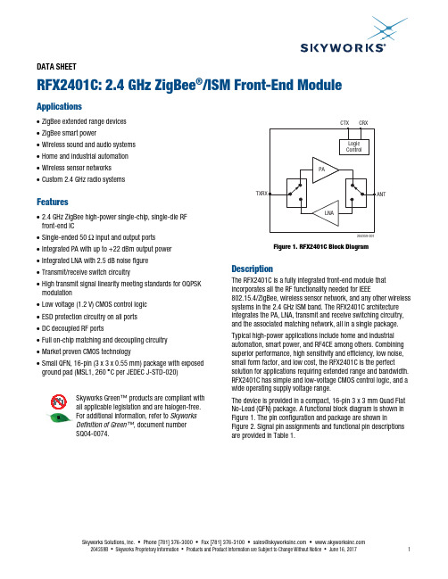
DATA SHEETRFX2401C: 2.4 GHz ZigBee ®/ISM Front-End ModuleApplications∙ ZigBee extended range devices ∙ ZigBee smart power∙ Wireless sound and audio systems ∙ Home and industrial automation ∙ Wireless sensor networks ∙ Custom 2.4 GHz radio systemsFeatures∙ 2.4 GHz ZigBee high-power single-chip, single-die RF front-end IC∙ Single-ended 50 Ω input and output ports ∙ Integrated PA with up to +22 dBm output power ∙ Integrated LNA with 2.5 dB noise figure ∙ Transmit/receive switch circuitry∙ High transmit signal linearity meeting standards for OQPSK modulation∙ Low voltage (1.2 V) CMOS control logic ∙ ESD protection circuitry on all ports ∙ DC decoupled RF ports∙ Full on-chip matching and decoupling circuitry ∙ Market proven CMOS technology∙ Small QFN, 16-pin (3 x 3 x 0.55 mm) package with exposed ground pad (MSL1, 260 ︒C per JEDEC J-STD-020)S kywork s G reen™ product s are compliant with all applicable legi s lation and are halogen-free.For additional information, refer to Skyworks Definition of Green™, document number S Q04-0074.204359-001Figure 1. RFX2401C Block DiagramDescriptionThe RFX2401C is a fully integrated front-end module that incorporates all the RF functionality needed for IEEE802.15.4/ZigBee, wireless sensor network, and any other wireless systems in the 2.4 GHz ISM band. The RFX2401C architecture integrates the PA, LNA, transmit and receive switching circuitry, and the associated matching network, all in a single package. Typical high-power applications include home and industrial automation, smart power, and RF4CE among others. Combining superior performance, high sensitivity and efficiency, low noise, small form factor, and low cost, the RFX2401C is the perfect solution for applications requiring extended range and bandwidth. RFX2401C has simple and low-voltage CMOS control logic, and a wide operating supply voltage range.The device is provided in a compact, 16-pin 3 x 3 mm Quad Flat No-Lead (QFN) package. A functional block diagram is shown in Figure 1. The pin configuration and package are shown inFigure 2. Signal pin assignments and functional pin descriptions are provided in Table 1.204359-002N/C G ND G ND TXRX TXENN/CVDD N/CG ND ANTG NDRXENN/C DN C VDD G ND1651234151413678910111217G NDFigure 2. RFX2401C Pinout(Top View)Table 1. RFX2401C Signal DescriptionsPin Name DescriptionPin Name Description1 N/C Not connected internally 9 GND Ground2GNDGround 10ANTConnect to 50 Ω antenna (DC shorted to GND) 3 GND Ground11 GND Ground4 TXRX RF signal to/from the transceiver (DC shorted to GND) 12 N/C Not connected internally5 TXEN CMOS input to control TX enable 13 DNC Do not connect6 RXEN CMOS input to control RX enable 14 VDD Alternate supply pin, internally connected to pin 167 N/C Not connected internally 15 N/C Not connected internally 8GNDGround16VDDVoltage supply connectionElectrical and Mechanical SpecificationsThe absolute maximum ratings of the RFX2401C are provided in Table 2. The recommended operating conditions are specified in Table 3. The electrical specifications are provided in Tables 4 and 5. The state of the RFX2401C is determined by the logic provided in Table 6.Table 2. RFX2401C Absolute Maximum Ratings1Parameter Conditions Minimum Maximum Units DC VDD voltage supply 0 4.0 VDC control pin voltage Through 1 kΩ resistor 0 3.6 VDC VDD current consumption Through VDD pins when TX is “ON” 350 mADC control pin current consumption 1 μATX RF input power All operating modes +5 dBmANT RF input power When RX is “ON” +5 dBmJunction temperature 150 °CStorage ambient temperature No RF and DC voltages applied -50 +150 o CElectrostatic discharge:Human Body Model (HBM) 3250 V 1Exposure to maximum rating conditions for extended periods may reduce device reliability. There is no damage to device with only one parameter set at the limit and all other parameters set at or below their nominal value. Exceeding any of the limits listed here may result in permanent damage to the device. All maximum RF input power ratings assume 50 Ω terminalimpedance.ESD HANDLING: Although this device is designed to be as robust as possible, electrostatic discharge (ESD) can damage this device.This device must be protected at all times from ESD when handling or transporting. Static charges may easily producepotentials of several kilovolts on the human body or equipment, which can discharge without detection.Industry-standard ESD handling precautions should be used at all times.Table 3. RFX2401C Recommended Operating Conditions1Parameter Conditions Min Typ Max Units DC VDD voltage supply All VDD pins 2.0 3.3 3.6 VControl voltage “high” Through 1 kΩ resistor 1.2 VDD VControl voltage “low” 0 0.3 VOperating ambient temperature Note 2 -40 +125o Cθja35o C/W1 During production test, devices will be tested at 5 V.2 For operation above +85 °C, use the θ ja as guidance for system design to assure the junction temperature will not exceed the maximum of +150 °C.Table 4. RFX2401C Electrical Specifications1 (V DD = 3.3 V, All Unused Ports Terminated with 50 Ω, T A = 25 °C, Unless Otherwise Noted) Parameter Symbol Test Condition Min Typ Max Units Frequency range f 2.4 2.525 GHz Transmit ModeSaturated output power +22 dBm Small-signalgain 21.5 25 26.5 dBSecond harmonic P OUT = +20 dBm, IEEE 802.15.4OQPSK modulation signal–10 dBm/MHzThird harmonic P OUT = +20 dBm, IEEE 802.15.4OQPSK modulation signal–20 dBm/MHzInput return loss –10 dBOutputreturnloss –6 dB Input / output impedance single-ended 50 ΩTX quiescent current No RF applied 17 mATX high-power current P OUT = +20 dBm 90 mALoad VSWR for stability (P OUT = +20 dBm) All non-harmonically related spursless than –43 dBm/MHz6:1 N/ALoad VSWR for ruggedness(P OUT = +20 dBm)No damage 10:1 N/A Receive ModeGain 12 dB Noisefigure 2.5 dB Input return loss –10 dBOutput return loss –12 dBRf port impedance 50 ΩRx quiescent current No RF applied 8 mAInput p1db At ANT pin –8 dBm1 Performance is guaranteed only under the conditions listed in this table.Table 5. RFX2401C Standby Mode Technical ParametersParameter Symbol Test Condition Min Typ Max Units DC shutdown current 1 μATXRX-ANT insertion loss (S21) Pin < -20 dBm –50 dBANT-TXRX insertion loss (S21) –50 dBReturn loss (S11) From TXRX port –1.5 dBTransmit-receive switchingtime 800 nsec Shutdown and “ON” State switchingtime 800 nsecTable 6. RFX2401C Control Logic1Mode TXEN RXENTX active 1 xRX active 0 1Shutdown 00 1 “1” denotes high voltage state (> 1.2 V)“0” denotes low voltage stage (< 0.3 V) at control pins“X” denotes do not care: either “1” or “0” can be appliedApplication Schematic Board DescriptionA suggested RFX2401C FEM application schematic diagram is shown in Figure 3. A schematic of the Evaluation Board is shown in Figure 4.Circuit Design ConsiderationsThe following design considerations are general in nature and must be followed regardless of final use or configuration:∙Paths to ground should be made as short as possible.∙If the transceiver TXRX port has DC present, use a capacitor to block this voltage from reaching the RFX2401C.∙The ground pad of the RFX2401C has special electrical and thermal grounding requirements. This pad is the main thermal conduit for heat dissipation. Because the circuit board acts as the heat sink, it must shunt as much heat as possible from the device.Multiple vias to the grounding layer are e thermal vias to assure efficient heat dissipation. ∙Locate the bypass capacitors as close as possible to the ground pad. Use two ground vias.∙The VDD (pin 14) is an optional VDD pin, internally connected to pin 16.∙The N/C pins 1, 7, 12, and 15 may be left open or connected to GND.∙If the antenna circuits have DC present, use a capacitor to block this voltage from reaching the RFX2401C.NOTE: A poor connection between the ground pad and ground increases junction temperature (T J), which reduces the lifeof the device..J4Figure 3. RFX2401C Application SchematicMA J2SFigure 4. RFX2401C Evaluation Board SchematicPackage DimensionsThe PCB layout footprint for the RFX2401C is shown in Figure 5. Typical part markings are shown in Figure 6. Package dimensions are shown in Figure 7, and tape and reel dimensions are provided in Figure 8.Package and Handling InformationInstructions on the shipping container label regarding exposure to moisture after the container seal is broken must be followed. Otherwise, problems related to moisture absorption may occur when the part is subjected to high temperature during solder assembly.The RFX2401C is rated to Moisture Sensitivity Level 1 (MSL1) at 260 C. It can be used for lead or lead-free soldering. For additional information, refer to the Skyworks Application Note, Solder Reflow Information , document number 200164. Care must be taken when attaching this product, whether it is done manually or in a production solder reflow environment. Production quantities of this product are shipped in a standard tape and reel format.204359-0040.5mm0.25mmFigure 5. RFX2401C PCB Layout Footprint(Top View)204359-006S kywork s Part Number Lot C odeDate C odePin 1Figure 6. Typical Part Markings(Top View)9-007Figure 7. RFX2401C Package DimensionsAll measurements are in millimeters.204359-0083.30 ±0.10Figure 8. RFX2401C Tape and Reel DimensionsDATA SHEET • RFX2401C: 2.4 GHz ZIGBEE/ISM FRONT-END MODULEOrdering InformationModel Name Manufacturing Part Number Evaluation Board Part Number RFX2401C: 2.4 GHz ZigBee/ISM Front-End Module RFX2401C RFX2401C-EK1Copyright © 2016-2017 Skyworks Solutions, Inc. All Rights Reserved.Information in this document is provided in connection with Skyworks Solutions, Inc. (“Skyworks”) products or services. These materials, including the information contained herein, are provided by Skyworks as a service to its customers and may be used for informational purposes only by the customer. Skyworks assumes no responsibility for errors or omissions in these materials or the information contained herein. Skyworks may change its documentation, products, services, specifications or product descriptions at any time, without notice. Skyworks makes no commitment to update the materials or information and shall have no responsibility whatsoever for conflicts, incompatibilities, or other difficulties arising from any future changes.No license, whether express, implied, by estoppel or otherwise, is granted to any intellectual property rights by this document. Skyworks assumes no liability for any materials, products or information provided hereunder, including the sale, distribution, reproduction or use of Skyworks products, information or materials, except as may be provided in Skyworks Terms and Conditions of Sale.THE MATERIALS, PRODUCTS AND INFORMATION ARE PROVIDED “AS IS” WITHOUT WARRANTY OF ANY KIND, WHETHER EXPRESS, IMPLIED, STATUTORY, OR OTHERWISE, INCLUDING FITNESS FOR A PARTICULAR PURPOSE OR USE, MERCHANTABILITY, PERFORMANCE, QUALITY OR NON-INFRINGEMENT OF ANY INTELLECTUAL PROPERTY RIGHT; ALL SUCH WARRANTIES ARE HEREBY EXPRESSLY DISCLAIMED. SKYWORKS DOES NOT WARRANT THE ACCURACY OR COMPLETENESS OF THE INFORMATION, TEXT, GRAPHICS OR OTHER ITEMS CONTAINED WITHIN THESE MATERIALS. SKYWORKS SHALL NOT BE LIABLE FOR ANY DAMAGES, INCLUDING BUT NOT LIMITED TO ANY SPECIAL, INDIRECT, INCIDENTAL, STATUTORY, OR CONSEQUENTIAL DAMAGES, INCLUDING WITHOUT LIMITATION, LOST REVENUES OR LOST PROFITS THAT MAY RESULT FROM THE USE OF THE MATERIALS OR INFORMATION, WHETHER OR NOT THE RECIPIENT OF MATERIALS HAS BEEN ADVISED OF THE POSSIBILITY OF SUCH DAMAGE.Skyworks products are not intended for use in medical, lifesaving or life-sustaining applications, or other equipment in which the failure of the Skyworks products could lead to personal injury, death, physical or environmental damage. Skyworks customers using or selling Skyworks products for use in such applications do so at their own risk and agree to fully indemnify Skyworks for any damages resulting from such improper use or sale.Customers are responsible for their products and applications using Skyworks products, which may deviate from published specifications as a result of design defects, errors, or operation of products outside of published parameters or design specifications. Customers should include design and operating safeguards to minimize these and other risks. Skyworks assumes no liability for applications assistance, customer product design, or damage to any equipment resulting from the use of Skyworks products outside of stated published specifications or parameters.Skyworks and the Skyworks symbol are trademarks or registered trademarks of Skyworks Solutions, Inc., in the United States and other countries. Third-party brands and names are for identification purposes only, and are the property of their respective owners. Additional information, including relevant terms and conditions, posted at , are incorporated by reference.SkyworksSolutions,Inc.•Phone[781]376-3000•Fax[781]376-3100•*********************•204359B • Skyworks Proprietary Information • Products and Product Information are Subject to Change Without Notice • June 16, 2017 11Mouser ElectronicsAuthorized DistributorClick to View Pricing, Inventory, Delivery & Lifecycle Information:S kyworks:RFX2401C RFX2401C-EK1。
MAX3250 3.0V-5.5V 加 isolation RS-232 通信接口评价包说明书

MAX3250±50V Isolated, 3.0V to 5.5V, 250kbps,2 Tx/2 Rx, RS-232 TransceiverEVALUATION KIT AVAILABLEGeneral DescriptionThe MAX3250 is a 3.0V to 5.5V powered, ±50V isolated EI A/TI A-232 and V.28/V.24 communications interface with high data-rate capabilities. The MAX3250 is a dual die part that operates with up to ±50V difference between the RS-232 side and the logic side (ISOCOM to GND). This makes the device ideal for operation in noisy conditions with high common-mode voltages.This feature prevents damage to the device if RS-232lines are inadvertently short-circuited to a +24V or ±48V power bus.The MAX3250 is powered by a single 3V to 5.5V supply on the logic side. Power is transferred from the logic side to the isolated side by ±100V external capacitors.The MAX3250 has two receivers (Rx) and two drivers (Tx) and is guaranteed to run at data rates of 250kbps while maintaining RS-232 output levels. The trans-ceivers have a proprietary low-dropout transmitter out-put stage, delivering true RS-232 performance from a 3V to 5.5V supply with a dual charge pump. The device features a FAULT open-drain output to signal an exces-sive isolated-side voltage condition on any of the RS-232 inputs. This output can drive an alarm LED or can be monitored by the processor to prevent operation under these conditions. The receiver outputs are high impedance in shutdown, allowing multiple interfaces (I rDA, RS-232, RS-485) to be connected to the same UART.The MAX3250 is available in a space-saving 28-pin SSOP package.ApplicationsIndustrial ControlProgrammable Logic Controller Point-of-Sale Equipment PC-to-Router Connections Diagnostic Ports Telecom EquipmentBenefits and Features•Isolation Breaks Ground Loops Due to High Common-Mode Voltages While Maintaining Data Rate •±50V Isolation•250kbps Guaranteed Data Rate•FAULT Output Signals Excessive Isolated-Side Voltage•Integration of Isolation and RS-232 Saves Space•SSOP Package•Shutdown Allows Multiple Interfaces (IrDA, RS-232,RS-485) to be Connected to the Same UART •High-Impedance Transmitter and Receiver Outputs in Shutdown•20µA Supply Current in Shutdown•Inductorless/Transformerless Design Simplifies EMI Compliance •Low-Cost Replacement for Opto-Isolated Transceivers •Meets EIA/TIA-232 Specifications Down to 3.0VTypical Operating Circuit appears at end of data sheet.Pin ConfigurationOrdering InformationAbsolute Maximum RatingsStresses beyond those listed under “Absolute Maximum Ratings” may cause permanent damage to the device. These are stress ratings only, and functional operation of the device at these or any other conditions beyond those indicated in the operational sections of the specifications is not implied. Exposure to absolute maximum rating conditions for extended periods may affect device reliability.(All voltages referenced to GND, unless otherwise noted.)V CC ...........................................................................-0.3V to +6VISOCOM...............................................................................±80V ISOVCC to ISOCOM.................................................-0.3V to +6V V+ to ISOCOM (Note 1)............................................-0.3V to +7V V- to ISOCOM (Note 1)............................................+0.3V to -7V V+ + |V-| (Note 1)...................................................................13V Input VoltagesT_IN, SHDN ...........................................................-0.3V to +6VR_IN to ISOCOM...............................................................±25VOutput VoltagesT_OUT to ISOCOM ........................................................±13.2VR_OUT.....................................................-0.3V to (V CC + 0.3V)FAULT ....................................................................-0.3V to +6V C1-, C2-......................................................-0.3V to (V CC + 0.3V)C1+, C2+, C3+, C3-, C4+, C4- to ISOCOM .....................................-0.3V to (ISOVCC + 0.3V)T_OUT Current..............30mA (continuous), 50mA (peak, 10µs)R_IN Current..................30mA (continuous), 50mA (peak, 10µs)ISOCOM Current...........30mA (continuous), 50mA (peak, 10µs)Short-Circuit Duration T_OUT to ISOCOM.................Continuous Continuous Power Dissipation (T A = +70°C)28-Pin SSOP (derate 15mW/°C above +70°C).......1201.2mW Operating Temperature Ranges MAX3250CAI .....................................................0°C to +70°C MAX3250EAI...................................................-40°C to +85°C Storage Temperature Range.............................-65°C to +150°C Lead Temperature (soldering, 10s).................................+300°C Soldering Temperature (reflow).......................................+260°C Electrical CharacteristicsNote 1:V+ and V- can have a maximum magnitude of 7V, but their absolute difference cannot exceed 13V.Electrical Characteristics (continued)Timing CharacteristicsNote 3:Transmitter skew is measured at the transmitter zero crosspoints.Typical Operating Characteristics(V CC = 3.3V, 250kbps data rate, see Typical Operating Circuit and Table 1 for capacitor values, all transmitters loaded with 3k Ωand C L to ISOCOM, T A = +25°C, unless otherwise noted.)TEMPERATURE (°C)S U P P L Y C U R R E N T (μA )603510-15-200-1000100200300400-300-4085SHUTDOWN CURRENT vs. TEMPERATURETIME TO EXIT SHUTDOWNV ISOCOM = 0V TOUT 5V/divMAX3250 toc04100μs/divSHDN 5V/divLOAD CAPACITANCE (pF)S U P P L Y C U R R E N T (m A )4000300020001000102030405060708090005000OPERATING SUPPLY CURRENT vs. LOAD CAPACITANCELOAD CAPACITANCE (pF)S L E W R A T E (V /μs )400030002000100051015202530005000SLEW RATEvs. LOAD CAPACITANCELOAD CAPACITANCE (pF)T R A N S M I T T E R O U T P U T V O L T A G E (V )4000300020001000-4-202468-65000TRANSMITTER OUTPUT VOLTAGEvs. LOAD CAPACITANCECOMMON-MODE FAULT RESPONSEISOCOM 50V/divMAX3250 toc07FAULT 5V/div4ms/divLOAD CAPACITANCE (pF)T R A N S M I T T E R O U T P U T V O L T A G E (V )4000300020001000-4-202468-65000TRANSMITTER OUTPUT VOLTAGEvs. LOAD CAPACITANCEDetailed DescriptionThe MAX3250 is a 3.0V to 5.5V powered, ±50V isolated EI A/TI A-232 and V.28/V.24 communications interface with high data-rate capabilities. The MAX3250 is a dual die part that operates with up to ±50V difference between the RS-232 side and the logic side (ISOCOM to GND). This makes the device ideal for operation in noisy conditions with high common-mode voltages. This feature prevents damage to the device if RS-232 lines are inadvertently short-circuited to a +24V or ±48V power bus.The MAX3250 typically draws 15mA of supply current when unloaded. Supply current drops to 20µA when the device is placed in shutdown mode. The MAX3250 has two receivers and two drivers and is guaranteed to operate at data rates up to 250kbps. The device features a FAULT open-drain output to signal an excessive isolated-side voltage condition on any of the RS-232 inputs. This output can drive an alarm LED or can be monitored by the processor to prevent operation under these conditions. The receiver outputs are high impedance in shutdown, allowing multiple interfaces (I rDA, RS-232, RS-485) to be connected to the same UART (Figure 1). The MAX3250 is a low-cost replacement for opto-isolated transceivers.Isolated Power SupplyThe MAX3250 drives a high-frequency square wave into C1 and a complementary square wave into C2. TheseFigure 1. Functional DiagramAC waveforms are rectified on the isolated side of the dual die to power its internal circuitry (I SOVCC). Capacitor C6 filters the output of the rectifier. See the Typical Operating Circuit.The power controller works in a dual power mode. Power is maximum when the isolated power supply is below its regulation point. Power is reduced when the isolated power supply is above its regulation point.Dual Charge-Pump Voltage ConverterThe RS-232 drivers are powered from a regulated dual charge pump that provides output voltages of +5.5V (dou-bling charge pump) and -5.5V (inverting charge pump) relative to ISOCOM over the 3.0V to 5.5V V CC range.The charge pumps are powered from I SOVCC and operate in a discontinuous mode. If the output voltages are less than 5.5V, the charge pumps are enabled. I f the output voltages exceed 5.5V, the charge pumps are disabled. Each charge pump requires a flying capacitor (C3, C4) and a reservoir capacitor (C7, C8) to generate the V+ and V- supplies.RS-232 TransmittersThe transmitters are inverting level translators that convert TTL/CMOS-logic levels to ±5.0V EI A/TI A-232-compliant levels. They guarantee a 250kbps data rate with worst-case loads of 3kΩin parallel with 1000pF to ISOCOM. In shutdown, the transmitters are disabled and the outputs are forced into a high-impedance state. When powered off or shut down, the outputs can be driven up to ±12V relative to I SOCOM. The transmitter inputs do not have pullup resistors. All unused inputs should be connected to V CC or GND.RS-232 ReceiversThe receivers convert RS-232 signals to CMOS-logic output levels. The receivers’ outputs are forced into a high-impedance state when the device is in shutdown. This allows a single UART to multiplex between differ-ent protocols.Low-Power Shutdown ModeShutdown mode is obtained by driving SHDN low. I n shutdown, the devices typically draw only 20µA of sup-ply current and no power is transferred across the iso-lation capacitors. The charge pumps are disabled, and the receiver outputs and transmitter outputs are high impedance. When exiting shutdown the charge pumps and transmitter outputs are fully operational in typically 500µs (Figure 3). Connect SHDN to V CC if the shut-down mode is not used.Applications InformationPower Isolation CapacitorsThe values for capacitors C1 and C2 are important for proper operation of the device. These capacitors should be 0.047µF for 4.5V to 5.5V operation, and 0.47µF for 3.0V to 3.6V operation. Smaller values result in insufficient supply voltage on the isolated side. Larger values are not allowed.Capacitor C9 provides an AC feedback path for proper controller operation. Connect C9 from ISOCOM to GND. The values for C1, C2, and C9 determine the maximum frequency and amplitude of the voltage difference between the local and isolated ground. Table 1 shows proper capacitance values.Figure 2. Transmitter Output Voltage vs. Load Current per Transmitter100µs/divV CC = 3.3VFigure 3. Transmitter Outputs when Exiting Shutdown or Powering UpTo achieve full isolation capability, C1, C2, and C9 should be rated for 100V or higher operation and be X7R or X5R type or metalized film dielectric. Y5V and Z5U dielectrics should be avoided as their voltage and tem-perature coefficients make their power-transfer capabili-ties insufficient.Charge-Pump and Bypass Capacitors Capacitors C3–C8 should be X7R or X5R type dielec-tric. Their voltage rating needs to be 10V or higher. Layout InformationBecause the MAX3250 is intended for systems requir-ing ±50V isolation, some consideration in component placement is necessary.A 20mil air gap should isolate the logic side and the isolated RS-232 side, across the N.C. pins (pin num-bers 6, 7, 22, and 23) of the MAX3250. The only com-ponents that cross this air gap should be C1, C2, and C9, which should all have a minimum 100V rating.All capacitors should be located as close to the MAX3250 as possible.Maximum Voltage BetweenISOCOM and Logic GNDHigh values of applied isolation voltage and frequency can cause ripple on I SOVCC, V+, V-, and in extreme cases on V CC. Therefore, it is recommended that the isolation-voltage and frequency be limited to the values shown in the Typical Operating Characteristics.I nsert a 1kΩ1/4W resistor in series with any isolation test voltage when testing for maximum values of applied isolation voltage. Exceeding the maximum lim-its of voltage and frequency (see the Typical Operating Characteristics) could trigger a holding current in the internal ESD-protection device if the ±80V isolation limit is exceeded. This resistor should not be used in normal application.Transmitter Outputs whenExiting ShutdownFigure 3 shows two transmitter outputs when exiting shutdown mode. As they become active, the two trans-mitter outputs are shown going to opposite RS-232 lev-els (one transmitter input is high, the other is low). Each transmitter is loaded with 3kΩin parallel with 2500pF. The transmitter outputs display no ringing or undesir-able transients as they come out of shutdown. Note that the transmitters are enabled only when the magnitude of V- exceeds approximately -3V.Chip InformationPROCESS: BiCMOSTypical Operating CircuitPackage InformationFor the latest package outline information and land patterns (foot-prints), go to /packages . Note that a“+”, “#”, or “-” in the package code indicates RoHS status only.Package drawings may show a different suffix character, but the drawing pertains to the package regardless of RoHS status.Revision HistoryFor pricing, delivery, and ordering information, please contact Maxim Direct at 1-888-629-4642, or visit Maxim Integrated’s website at . Maxim Integrated cannot assume responsibility for use of any circuitry other than circuitry entirely embodied in a Maxim Integrated product. No circuit patent licenses are implied. Maxim Integrated reserves the right to change the circuitry and specifications without notice at any time. The parametric values (min and max limits) shown in the Electrical Characteristics table are guaranteed. Other parametric values quoted in this data sheet are provided for guidance.。
LM385M3-1.2中文资料

LM185-1.2/LM285-1.2/LM385-1.2Micropower Voltage Reference DiodeGeneral DescriptionThe LM185-1.2/LM285-1.2/LM385-1.2are micropower 2-terminal band-gap voltage regulator diodes.Operating over a 10µA to 20mA current range,they feature exception-ally low dynamic impedance and good temperature stability.On-chip trimming is used to provide tight voltage tolerance.Since the LM185-1.2band-gap reference uses only transis-tors and resistors,low noise and good long term stability re-sult.Careful design of the LM185-1.2has made the device ex-ceptionally tolerant of capacitive loading,making it easy to use in almost any reference application.The wide dynamic operating range allows its use with widely varying supplies with excellent regulation.The extremely low power drain of the LM185-1.2makes it useful for micropower circuitry.This voltage reference can be used to make portable meters,regulators or general purpose analog circuitry with battery life approaching shelf life.Further,the wide operating current allows it to replace older references with a tighter tolerance part.The LM185-1.2is rated for operation over a −55˚C to 125˚C temperature range while the LM285-1.2is rated −40˚C to 85˚C and the LM385-1.20˚C to 70˚C.The LM185-1.2/LM285-1.2are available in a hermetic TO-46package and the LM285-1.2/LM385-1.2are also available in a low-cost TO-92molded package,as well as SO and SOT-23.The LM185-1.2is also available in a hermetic leadless chip car-rier package.Featuresn ±4mV (±0.3%)max.initial tolerance (A grade)n Operating current of 10µA to 20mA n 0.6Ωmax dynamic impedance (A grade)n Low temperature coefficientn Low voltage reference —1.235Vn 2.5V device and adjustable device also available nLM185-2.5series and LM185series,respectivelyConnection DiagramsT0-92Plastic Package (Z)DS005518-10Bottom ViewOrder Number LM285Z-1.2,LM285BXZ-1.2,LM285BYZ-1.2LM385Z-1.2,LM385BZ-1.2LM385BXZ-1.2or LM385BYZ-1.2See NS Package Number Z03ASOT23DS005518-33*Pin 3is attached to the Die Attach Pad (DAP)and should be connected to Pin 2or left floating.Order Number LM385M3-1.2See NS Package Number MA03BJanuary 2000LM185-1.2/LM285-1.2/LM385-1.2Micropower Voltage Reference Diode©2000National Semiconductor Corporation Connection Diagrams(Continued)SO PackageDS005518-9Order Number LM285M-1.2,LM285BXM-1.2,LM285BYM-1.2LM385M-1.2,LM385BM-1.2LM385BXM-1.2or LM385BYM-1.2See NS Package Number M08ATO-46Metal Can Package (H)DS005518-6Bottom ViewOrder Number LM185H-1.2,LM185H-1.2/883,LM185BXH-1.2,LM185BYH-1.2LM285H-1.2or LM285BXH-1.2See NS Package Number H02AL M 185-1.2/L M 285-1.2/L M 385-1.2 2Absolute Maximum Ratings(Note1)If Military/Aerospace specified devices are required, please contact the National Semiconductor Sales Office/ Distributors for availability and specifications.(Note2)Reverse Current30mA Forward Current10mA Operating Temperature Range(Note3)LM185-1.2−55˚C to+125˚C LM285-1.2−40˚C to+85˚C LM385-1.20˚C to70˚C Storage Temperature−55˚C to+150˚C Soldering InformationTO-92package:10sec.260˚C TO-46package:10sec.300˚C SO and SOT Pkg.Vapor phase(60sec.)215˚C Infrared(15sec.)220˚C See AN-450“Surface Mounting Methods and Their Effecton Product Reliability”for other methods of soldering surface mount devices.Electrical Characteristics(Note4)LM185-1.2LM185BX-1.2LM385B-1.2LM185BY-1.2LM385BX-1.2LM385-1.2LM285-1.2LM385BY-1.2Units Parameter Conditions Typ LM285BX-1.2(Limit)LM285BY-1.2Tested Design Tested Design Tested DesignLimit Limit Limit Limit Limit Limit(Notes5,8)(Note6)(Note5)(Note6)(Note5)(Note6)Reverse Breakdown T A=25˚C, 1.235 1.223 1.223 1.205V(Min) Voltage10µA≤I R≤20mA 1.247 1.247 1.260V(Max) Minimum Operating8102015201520µACurrent LM385M3-1.21015(Max) Reverse Breakdown10µA≤I R≤1mA1 1.51 1.51 1.5mVVoltage Change(Max)with Current1mA≤I R≤20mA102020252025mV(Max) Reverse Dynamic I R=100µA,f=20Hz1ΩImpedanceWideband Noise I R=100µA,60µV(rms)10Hz≤f≤10kHzLong Term Stability I R=100µA,T=1000Hr,20ppm T A=25˚C±0.1˚CAverage Temperature I R=100µACoefficient(Note7)X Suffix3030ppm/˚C Y Suffix5050ppm/˚CAll Others150150150ppm/˚C(Max)Note1:Absolute Maximum Ratings indicate limits beyond which damage to the device may occur.Operating Ratings indicate conditions for which the device is in-tended to be functional,but do not guarantee specific performance limits.For guaranteed specifications and test conditions,see the Electrical Characteristics.The guaranteed specifications apply only for the test conditions listed.Note2:Refer to RETS185H-1.2for military specifications.Note3:For elevated temperature operation,T j max is:LM185150˚CLM285125˚CLM385100˚CThermal Resistance TO-92TO-46SO-8SOT23θJA(junction to ambient)180˚C/W(0.4"leads)440˚C/W165˚C/W283˚C/W170˚C/W(0.125"leads)θJC(junction to case)N/A80˚C/W N/A N/ANote4:Parameters identified with boldface type apply at temperature extremes.All other numbers apply at T A=T J=25˚C.LM185-1.2/LM285-1.2/LM385-1.23Electrical Characteristics (Note 4)(Continued)Note 5:Guaranteed and 100%production tested.Note 6:Guaranteed,but not 100%production tested.These limits are not used to calculate average outgoing quality levels.Note 7:The average temperature coefficient is defined as the maximum deviation of reference voltage at all measured temperatures between the operating T MAX and T MIN ,divided by T MAX −T MIN .The measured temperatures are −55˚C,−40˚C,0˚C,25˚C,70˚C,85˚C,125˚C.Note 8:A military RETS electrical specification is available on request.Typical Performance CharacteristicsReverse CharacteristicsDS005518-13Reverse CharacteristicsDS005518-14Forward CharacteristicsDS005518-15Temperature Drift of 3Representative UnitsDS005518-16Reverse Dynamic Impedance DS005518-17Reverse Dynamic ImpedanceDS005518-18Noise Voltage DS005518-19Filtered Output Noise DS005518-20Response TimeDS005518-21L M 185-1.2/L M 285-1.2/L M 385-1.2 4Typical ApplicationsWide Input Range ReferenceDS005518-8Micropower Referencefrom 9V BatteryDS005518-22Reference from 1.5V BatteryDS005518-23Micropower *5V Regulator DS005518-24*I Q ≅30µAMicropower *10V ReferenceDS005518-25*I Q ≅20µA standby currentPrecision 1µA to 1mA Current SourcesDS005518-26DS005518-27LM185-1.2/LM285-1.2/LM385-1.25Typical Applications(Continued)METER THERMOMETERS0˚C−100˚C ThermometerDS005518-28Calibration1.Short LM385-1.2,adjust R3for I OUT =temp at 1µA/˚K2.Remove short,adjust R2for correct reading in centigrade †I Q at 1.3V ≅500µA I Q at 1.6V ≅2.4mALower Power ThermometerDS005518-29*2N3638or 2N2907select for inverse H FE ≅5†Select for operation at 1.3V ‡I Q ≅600µA to 900µA0˚F−50˚F ThermometerDS005518-30Calibration1.Short LM385-1.2,adjust R3for I OUT =temp at 1.8µA/˚K2.Remove short,adjust R2for correct reading in ˚FMicropower Thermocouple Cold JunctionCompensatorDS005518-31Adjustment Procedure1.Adjust TC ADJ pot until voltage across R1equals Kelvin temperature multiplied by the thermocouple Seebeck coefficient.2.Adjust zero ADJ pot until voltage across R2equals the thermocouple Seebeck coefficient multiplied by 273.2.ThermocoupleSeebeck R1R2Voltage Voltage TypeCoefficient (Ω)(Ω)Across R1Across R2(µV/˚C)@25˚C(mV)(mV)J 52.35231.24k 15.6014.32T 42.84321k12.7711.78K 40.8412953Ω12.1711.17S6.463.4150Ω1.9081.766Typical supply current 50µAL M 185-1.2/L M 285-1.2/L M 385-1.2 6Typical Applications(Continued)Schematic DiagramCentigrade ThermometerDS005518-1Calibration1.Adjust R1so that V1=temp at 1mV/˚K2.Adjust V2to 273.2mV†I Q for 1.3V to 1.6V battery volt-age =50µA to 150µADS005518-7LM185-1.2/LM285-1.2/LM385-1.27Physical Dimensionsinches (millimeters)unless otherwise notedTO-46Metal Can Package (H)Order Number LM185H-1.2,LM185H-1.2/883,LM185BXH-1.2,LM185BYH-1.2,LM285H-1.2,or LM285BXH-1.2NS Package Number H02ASOT-23Package (M3)Order Number LM385M3-1.2NS Package Number MA03BL M 185-1.2/L M 285-1.2/L M 385-1.28Physical Dimensionsinches (millimeters)unless otherwise noted (Continued)Small Outline (SO-8)PackageOrder Number LM285M-1.2,LM285BXM-1.2,LM285BYM-1.2LM385M-1.2,LM385BM-1.2,LM385BXM-1.2,LM385BYM-1.2NS Package Number M08ATO-92Plastic Package (Z)Order Number LM285Z-1.2,LM285BXZ-1.2LM285BYZ-1.2,LM385Z-1.2,LM385BZ-1.2LM385BXZ-1.2or LM385BYZ-1.2NS Package Number Z03ALM185-1.2/LM285-1.2/LM385-1.29NotesLIFE SUPPORT POLICYNATIONAL’S PRODUCTS ARE NOT AUTHORIZED FOR USE AS CRITICAL COMPONENTS IN LIFE SUPPORT DEVICES OR SYSTEMS WITHOUT THE EXPRESS WRITTEN APPROVAL OF THE PRESIDENT AND GENERAL COUNSEL OF NATIONAL SEMICONDUCTOR CORPORATION.As used herein:1.Life support devices or systems are devices or systems which,(a)are intended for surgical implant into the body,or (b)support or sustain life,and whose failure to perform when properly used in accordance with instructions for use provided in the labeling,can be reasonably expected to result in a significant injury to the user.2.A critical component is any component of a life support device or system whose failure to perform can be reasonably expected to cause the failure of the life support device or system,or to affect its safety or effectiveness.National Semiconductor Corporation AmericasTel:1-800-272-9959Fax:1-800-737-7018Email:support@National Semiconductor EuropeFax:+49(0)180-5308586Email:europe.support@Deutsch Tel:+49(0)180-5308585English Tel:+49(0)180-5327832Français Tel:+49(0)180-5329358Italiano Tel:+49(0)180-5341680National Semiconductor Asia Pacific Customer Response Group Tel:65-2544466Fax:65-2504466Email:sea.support@National Semiconductor Japan Ltd.Tel:81-3-5639-7560Fax:81-3-5639-7507L M 185-1.2/L M 285-1.2/L M 385-1.2M i c r o p o w e r V o l t a g e R e f e r e n c e D i o d eNational does not assume any responsibility for use of any circuitry described,no circuit patent licenses are implied and National reserves the right at any time without notice to change said circuitry and specifications.。
L11831A L11831B L11831C 友顺UTC 电子元器件芯片

Absolute maximum ratings are stress ratings only and functional device operation is not implied.
RECOMMENDED OPERATING CONDITIONS (Note 1)
PARAMETER Supply Voltage Control Voltage (VDD≥VOUT+1.5V) Ambient Temperature Range Junction Temperature Range
Package
HSOP-8 DFN3030-10
CMOS IC
Packing Tape Reel Tape Reel
Copyright © 2022 Unisonic Technologies Co., Ltd
1 of 6
QW-R502-A88.M
L11831A/B/C
MARKING INFORMATION
Dropout Voltage (Note 3)
Quiescent Current (Note 4)
Current Limit
Short Circuit Current
VOUT Pull Low Resistance
Soft-Start
L11831C
VTH_ADJ VADJ ∆VOUT
∆VLINE_IN ∆VLOAD VDROP
TOPR
-40 ~ +85
°C
Storage Temperature
TSTG
-65 ~ +150
°C
Note: Absolute maximum ratings are those values beyond which the device could be permanently damaged.
电池规格书(Ni-MH SC2500mAh)
NI-MH BATTERYDELIVERY SPECIFICATIONS镍氢电池规格书******************PRESENTED TO(呈送):MODEL NO.(产品型号): Ni-MH SC2500mAh 1.2VDATE(制作日期): 20th July 2012 Customer Part No.(客户物料编码) :Add:地址:Postcode(邮编): http(网址):Tel(电话): Fax(传真):E-mail(邮箱):1. Scope (适用范围)This specification governs the performance of the following Nickel-Metal Hydride cylindricalbattery 。
本规格书适用于下述型号的可充性圆柱形镍氢电池。
2. Innovation model(亿诺型号):Ni-MH SC2500mAh 1.2V。
3. External Appearance(外观)The cell / battery shall be free from cracks, scars, breakage, rust,discoloration, leakage and deformation. 电池/电池组外观无破裂、划痕、变形、生锈、污迹、电解液泄漏等不良现象。
4. Ratings(规定参数)The data involving the nominal voltage and the approximate weight of the battery pack。
5. Performance(电池性能)Unless otherwise stated, tests should be done within one month of delivery under the following conditions: 除非其它规定,测试应在到货之日起1个月内进行,并且符合以下测试条件:Relative humidity(相对湿度):65±20%。
- 1、下载文档前请自行甄别文档内容的完整性,平台不提供额外的编辑、内容补充、找答案等附加服务。
- 2、"仅部分预览"的文档,不可在线预览部分如存在完整性等问题,可反馈申请退款(可完整预览的文档不适用该条件!)。
- 3、如文档侵犯您的权益,请联系客服反馈,我们会尽快为您处理(人工客服工作时间:9:00-18:30)。
C++ZZG(combata@) 2006-9-51第一章 OOP (1)1.1OOP 思想 (1)1.2OOPL (1)1.2.1 对象 (1)1.2.2 类 (1)1.2.3 消息 (1)1.2.4 子类 (1)1.2.5 类型参数化 (2)1.3OO 方法 (2)2第二章 C++对C非OO特特型扩展 (2)2.1C++输入输出 (2)2.1.1 继续使用C中I/O方法 (2)2.1.2 增加了新的I/O方法 (2)2.2new 和 delete (2)2.3const 说明符 (3)2.4缺省参数 (3)2.5引用 (3)2.5.1 独立引用 (3)2.5.2 传递引用 (3)2.5.3 返回引用 (4)2.6内联函数 (4)3第三章类 (4)3.1类和对象概述 (4)3.1.1 类和对象要点 (4)3.1.2 类和对象相关说明 (5)3.2构造函数和类的初始化 (5)3.2.1 带参数的构造函数 (5)3.2.2 重载构造函数 (6)3.2.3 拷贝构造函数 (6)3.2.4 类对象初始化(初始化列表/初始化值表)问题 (6)3.3关键字this和对象的自引用 (7)3.3.1 对象创建过程 (7)3.3.2 this指针 (7)3.4结构体 (8)3.4.1 结构体与类的区别 (8)3.4.2 结构体对齐、位断问题 (8)3.4.3 C中共同(联合)体与C++中没有共同体 (8)3.5静态成员和友元 (8)3.5.1 静态数据成员 (8)3.5.2 静态成员函数(类方法/类消息) (8)3.5.3 友元 (9)3.6对象数组 (9)3.6.1 一般形式的对象数组 (10)3.6.2 对象指针数组 (10)3.6.3 类数据成员的指针数组 (10)3.6.4 建立类的数据成员 (10)4第四章运算符重载 (11)4.1基本概念 (11)4.1.1 重载运算符的方法 (11)4.1.2 运算符函数的基本格式 (11)4.2一元和二元运算符 (11)4.2.1 一元运算符 (11)4.2.2 二元运算符 (12)5第五章子类,继承性,多态性 (13)5.1子类 (13)5.1.1 子类定义格式 (13)5.1.2 子类中的静态成员 (13)5.1.3 访问声明(用于私有派生) (14)5.2类等级中基类的初始化 (14)5.2.1 子类构造函数的声明方式 (14)5.2.2 子类构造函数的定义 (14)5.3继承性(多重继承和虚基类) (14)5.3.1 多重继承 (14)5.3.2 虚基类 (15)5.4多态性(虚函数的多态性) (16)5.4.1 多态性 (16)5.4.2 虚函数 (16)5.5纯虚函数和抽象类 (16)5.5.1 纯虚函数 (17)5.5.2 抽象类 (17)1第一章 OOP1.1OOP 思想面向过程面向对象使用传统软件工程开发方法. OOA(分析)/OOD(设计)思路封闭式策略开放式策略设计方法算法,任务分解对象分解编码语言非OOPL OOPL 支持四种机制(抽象、封装、继承、多态性) 特征供应者/使用者关系紧密较松、独立1.2OOPL1.2.1对象将数据和施加数据上的操作封装于一个实体内,则该实体称为对象.对象特点:是一个基本的封装单位(数据、操作、局部存储空间、局部处理).对象同外界联系方式:消息传递.注:对象具有状态,它体现了抽象.1.2.2类能够响应同一消息的对象就构成了一个类.a)类体现了有共同性质的一类事物(对象)的抽象自然界事物的两种关系:分类关系、组装关系b)类中的每个对象称为该类的一个实例c)类的两种视图-内部视图是类的实现、操作的实现细节.-外部视图是类的接口、用类的描述协议给出.注: 接口可见,具体如何实现不可见.d)类描述协议-私有数据:不同实例具有不同值的数据,用实例变量描述(private data).-共享数据:类中所有实例具有同一个值的数据,用类变量描述(share data).-全程共享数据:有几个类共享数据.(全程量)-消息:操作、方法.1.2.3消息消息即同名操作、封装在类(对象)内部.操作分为:实例方法:一个类的实例对象响应的消息对应操作.类方法(静态方法):对全体对象操作方法.注: 消息对应不同原型的函数名(方法名).1.2.4子类类有层次结构子类:在一个类的范围内划分的类父类:若A是B的子类,称B是A的父类.性质:父类的性质(属性、方法)可以继承给子类;此外子类可以具有自己特有的性质(共性与个性关系).a)继承性: 一个类实例对象的性质可以从他的父类中继承-消息的继承.-数据(部分)的继承.-单继承/多继承.b)多态性: 不同的对象(有一定继承关系)对同一个消息做出适合自己的不同的响应-编译时多态性:函数重载.-运行时多态性:多态性/动态.1.2.5 类型参数化参数表示类型,最后再定(类模版) 1.3 OO 方法编码任务分析设计2 第二章 C++对C 非OO 特特型扩展2.1 C++输入输出2.1.1 继续使用C 中I/O 方法 2.1.2 增加了新的I/O 方法a) 用cout 表示标准输出流,cin 表示标准输入流 b) 用两个相关的运算符<<把其后的参数写到cout.>>将cin 读入数据到运算符后部的参数中. c) 要包含文件 iostream.h 例: # include <iostream.h>main(){int inch=0; cout<<”inchs=”; cin>> inch; cout<<”in=”; cout<<inch*2.54; cout<<”cm”; }2.2 new 和 deletemalloc() 和free()必须成对使用. new:动态内存空间分配. delete:动态内存空间释放. 一般格式: p=new type; delete p; 例: #include <iostream.h>main () {int *p; int *p; p=new int; p=new int[50]; *p=10; p[10]=10; cout<<*p; cout<<p[10]; delete p; delete []p}2.3const 说明符用于冻结它作用域范围内由const确定的值.a)用于定义类型化的常数(有地址与define不同)例: const int m=7;b)const与指针联用-指针说明前冠以const使指针所指的对象为常量.例: const char*p=”abcd”;p[2]=’x’ ; 错误 *p=”student”; 正确-用*const声明指针使指针成为常指针.例: char *const p=”abcd”;const char*const p=”abcd”; p[2]=”x”; 正确 *p=”student”; 错误-修饰类,类声明中的成员参数.2.4缺省参数例: void fun(int i=1){} //此处缺省值为1调用: f un(10); //传递10fun(); //自动给i缺省值1void xyout(char*str,int x=-1,int y=-1){if(x==-1)x=wherex(); //返回当前x的坐标值if(y==-1)y=wherey(); //返回当前y的坐标值gotoxy(x,y); //光标移动到(x,y)的位置cout<<str;}注: 所有缺省参数在形参中应排在非缺省的右方.2.5引用本质:共享一个存储单元定义:符号 Z&表示对Z类型的引用(Z不能是void及数组类型).含义:为Z类型的对象取一个别名.例: Z& y=z;建立一个Z类型的引用y,并将y初始化到对象(Z类型)z上(使z有一个别名y).2.5.1独立引用为一对象建立别名.例:int i;int& j=i;int k=q;j=k; //i=k int *q;int *&p=q;int b=3;p=&b; //q=&b;注:-独立引用必须在建立时初始化到一个对象. int i,k;int &j=i;-引用一旦有了对象,就不能再改变其联系对象. j=&k; //错误-有的语言可以将引用初始化到一个常量上.const int i=1;int& m=i;或const int& m=1;2.5.2传递引用将引用作为函数的形参(目的实现传名调用).例: 交换变量m,n的值void swap(int* p,int*q) {int t;t=*p;*p=*q;*q=t; }调用swap(&m,&n); void swap (int&a,int&b) {int t;t=a;a=b;b=t;}swap (m,n);2.5.3返回引用将一个函数的类型申明为引用,函数将返回函数返回值的地址单元.例: int& F1 (int*A,int&i){int&j=A[i];i=j/3;return(A[j]);}设int B[]={14,6,15,3,21,89,31,6}; int k=1;给出以下语句的含义F1 (B, k) =40;结果B[6]Å40,kÅ2 以下函数是否正确int& fun(){inti;//i局部自动类型变量,出来之后不存在(被收回) i=3;return(i);}规则:当函数返回值是指针或引用时,函数返回后,其所指的实体必须存在,因此,不能将函数返回值赋局部自动类型变量.2.6内联函数在函数说明前加”inline”其后的函数被指定的为内联函数.编译时,在调用内联函数的位置用它的函数体进行置换(类似于宏替换#define,定义有不同).宏替换形式#define abs (v) v<0?-v: v i=-1;调用abs(i++);即(i++)<0?- (i++) :( i++) -1 0 1 内联函数形式incline long abs (long i){return (i<0?-i: i) ;}(i++)<0?-(i++) :(i++)//若为内联函数所有(i++)为一个表达式//i=1;abs(i++);返回1,abs(++i);返回23第三章类3.1类和对象概述3.1.1类和对象要点在C++中类作为一种新类出现,使用时,先定义类,然后再创建该类型一个实例对象.一个C++完整程序a)类声明:.h文件b)主函数main(): 建立各类的实例对象;构成对象消息序列(基本功能语句)c)自由功能函数例: 一个串类的定义和使用类声明定义 class String { private: int length;char *content; public:String(); ~String(); int get_length() {return length; }char* get_content() {return content; }void set_content(int in_length,char*in_content); void set_content(char*in_content); }类实现(String.lib) String::String()//类区分符+类名Æ完全类标识符 {length=in_length; content=in_content; }String::set_content(char*in_content) {content=in_content;int i=0;while(*in_content++)i++; length=i;}使用文件(String.cpp) #include “String.h”main(){ String s1,s2;s1.set_content(“hello,world\n”); int i=s1.get_length(); cout<<”s1=”<<s1; }3.1.2 类和对象相关说明 a) 类声明/定义的一般格式class<类名>{//类外部视图:声明private://私有段(缺省段名):私有数据或函数(操作),只能被本例中声明的函数访问. protect://保护段:保护段数据或函数只能被本类及其子类中声明函数访问. public://共有段:共有段数据或函数被作用域内存在的任何函数或实体访问. }b) 在C++中类的操作成员称为成员函数一般的成员函数分为:构造及析构函数、查询函数、功能函数. c) 成员函数可以d) 构造函数与析构函数- 构造函数Æ创建对象(分配空间、对其初始化). - 析构函数Æ回收/释放对象.注: 两者既可由用户定义,也可缺省,系统自动使用该类缺省版本.构造函数可以有参数,析构函数不可以有参数. e) 操作对象的方法 从对象外部向对象发出消息. - 访问成员函数直接 对象名.成员函数(<实参表>). 间接 (指向对象)Æ成员函数(<实参表>). - 访问成员数据 类名::数据名 对象.数据名 f)属于同一个类的成员函数可以相互调用3.2 构造函数和类的初始化 3.2.1 带参数的构造函数功能:利用构造函数中的的参数为对象指定全域或部分属性值.(初始属性)在类内实现Æ被自动识别为内联在类外实现Æ在函数类型中使用完整函数名例: class pen{int color;public :pen(int c) {color=c;} }使用 pen p1,p2(red); 3.2.2 重载构造函数含义:定义一个类时,可以为该类设置多个构造函数;使得在生成类的实例对象时,能够产生不同属性的对象. 例: class Z{ public:Z(); Z(int); Z(int,char); } main() { Z a;//使用Z();Z b(1); //使用Z(int); Z c(1,c); //使用Z(int,char);} 注:a) 类型中不存在用户定义的构造函数时,C++将产生缺省的构造函数,系统自动调用构造函数,缺省的构造函数不带参数 b) 用户提供的构造函数中可以使用缺省参数,但这会导致二义性 Z();Z(int i=0); //尽可能避免使用,不知调用那一个构造函数. c) 构造函数被调用用于以下场合- 通过已定义的类创造一个新实例对象时. Z a; - 复制一个实例对象时.Z c=a;- 用new 动态产生实例对象时. 3.2.3 拷贝构造函数功能:当创建一个新对象时,利用这个构造函数把一个已存在对象的私有成员(数据成员)逐段拷贝到这个新对象. 格式:以自己所在类的引用作为一个函数参数. 例: class Z{ public: Z();Z(const Z&);//const 约束调用时与引用相关联的对象必定为常对象.}Z a; Z b=a; Z (a);//复制时,a 中数据不变,完全复制.class A{ public:A(int);A(const A&,int i=1);}使用: A a(10);A b(a,0); A c=b;//后两者都会使用拷贝构造函数产生b,c 对象复制.系统备有缺省的拷贝构造函数,当用户没有显示定义拷贝构造函数时,系统使用缺省拷贝构造函数,只有一个引用参数.A(const A&) 例: class String{… };String f(String s) {return s;}main() {String p=”abcd”; String t=f(p); }3.2.4 类对象初始化(初始化列表/初始化值表)问题 a) C++中表达式初始化方法- 继承C 中:使用初始值表(对数组;结构体等). int A[]={3,4,5,6,0};-继承C中:使用赋值表达式.int m=0;-使用”表达式表”(C++扩充).int m(0)ÅÆ int m=0;char *p(“abcd”); //ÅÆchar *p=”abcd”;b)类对象的初始化方法-利用类”表达式表”或复制表达式.-通过类的构造函数为类对象初始化.例: class Z{int i;p ublic:Z (); Z(int k); Z(const Z&);}利用表达式表: Z a(1); Z b(a);利用赋值表达式: Z c=1; ÅÆZ c=Z (1); Z d=a;c)对构造函数的实现时,如何对数据成员赋值-在函数体内赋值-在函数体外赋值例: class Z{a,b;intpublic:Z(int i,int j);{a=i;b=j;}}使用:Z (int i,int j):a(i),b(j){}3.3关键字this和对象的自引用3.3.1对象创建过程定义一个类创建一个类的实例对象例: class pen{int a,b,c,d;}3.3.2this指针-常指针,始终指向(将来的)消息接收者对象.-当一个类的实例对象创造时,this指针就立即初始化到该对象.-类的每个成员函数的参数表中,都会因含一个this指针参数,该函数调用时,作为消息接收者对象的this被传送到函数体中(并没有在形参表中,隐含着) .例: class A{int m;public:void fi(int i)m(i){}; //thisÆm=i;ÅÆ(*this).m=i;ÅÆ m(i){};ÅÆ {m=i};}使用:A a,b; a.f1(10); //其中a为消息接收者,f1(10)为消息.使用this指针可以实现对本类对象的自引用.例: 在一个双向链表中插入一个表项.class dlink{//声明一个表项类 dlinkfloat data;dlink *pre;dlink *suc;public:void append(dlink*p)//把p 所指的新类项添加到某一表项后 }void dlink::append(dlink*p) {p Æsuc=this Æsuc; //p Æsuc=suc; this Æsuc Æpre=p; //suc Æpre=p; this Æsuc=p; //suc=p; p Æpre=this; //p Æpre=this; }this 是一个常指针 this 和其所指对象稳固 const 成员函数 例: class Z{ public:int g()const; //const 成员函数,在const 成员函数的形参表中,隐含下列形式的this 指针: } 3.4 结构体3.4.1 结构体与类的区别 3.4.2 结构体对齐、位断问题3.4.3 C 中共同(联合)体与C++中没有共同体 3.5 静态成员和友元 3.5.1 静态数据成员 a) 类变量b) 类的所有实例对象都共享静态数据成员的值c) 静态数据成员在类中声明是纯声明,必须在类外进行初始化 例: class counter{static int n; //声明,没分配存储空间,没初始化 public: void set_count (int i) {n=i;}void show_count(){printf(“%d\n”,n);}}使用: int counter::n=0;//初始化 counter a,b;a.show_count();// return 0b.show_count();// return 0 a.set_count(10);a.show_count();// return 10b.show_count();// return 103.5.2 静态成员函数(类方法/类消息) a) 声明方式在成员函数类型定义前加static. b) 类方法静态成员函数的形参表中无隐含的this 指针参数. 在具体函数体内不得以任何形式出现this 指针. c) 使用主要用来访问静态数据成员或全局变量.用于处理类中的”自由子程序”Æ有类名(无数据成员,所有自由子程序置于公有类,设为静态成员函数).this 常指针this 常对象const Z*const this 指向常对象的常指针例: class Z{int m;public:static void func(int i, Z*p); } 使用:Z a,*q; init (a); q=&a;方式1: Z::func(10,&a); //常用调用方式,不能用于非静态成员函数. 方式2: a.func(10,&a); q Æfunc(10,&a); //消息发送方式. void Z::func(int i,Z*p) { m=i; //错误,m 不明确,应该p Æm=i or (*p).m=i. } 3.5.3 友元 a) 基本概念为了调节封装性(数据隐藏)带来的不便,通过定义一个类的友元,来实现对类中对象私有成员的访问. 友元可以是一个函数或类.使用(成员和友元的区别)权利一样,使用方法不一样. Z 友元函数的形参表中不含指向Z 对象的this 指针. b) 友元的声明方法Z 类的友元必须在Z 类内进行声明. 声明方法: -Y 是一个普通函数(定义在Z 外,声明在Z 中,放在Z 中那个段都一样).例: class Z{ int i;friend void f(int,Z*);//声明 }实现: void f(int k,Z*p)//定义 { p Æi=k;} -Y 是另一个类A 的成员函数.例: class A{ public: void f();} class Z{ int i; friend void A::f(); //f()是A 的成员函数. } -Y 是另一个类(把类A 作为Z 类友元类). 例: class A; class Z{ friend A;}class A{ public:void f1(…Z*); void f2(…Z*); }3.6 对象数组 要点:对带有构造函数的类才能建立起对应数组.对象数组的元素均是同一类的实例对象.构成对象数组类必须有一个不带参数的构造函数(即数组中对象初始值相同).3.6.1一般形式的对象数组例: class value{int v;public:value(){v=0;}v alue(int u){v=u;}// ÅÆvalue(int u):v(u){}i nt get value(){return u;}v oid set value(){v=u;}}value bills[10];//调用value()为每个数组元素初始化.value coins[10]={0,1,2,…,9};//调用value(int u)为每个数组元素初始化.3.6.2对象指针数组产生方法1 value * p[3]={new value(0);newvalue(1);newvalue(2);}产生方法2 value*coins[3];for(i=0;i<3;i++)coins[i]=new value;classsomedata{public:int data;somedata(){data=0;}somedata(int d){data=d;}}somedatad1(15),d2;intstuff[3]={d1.data,d2.data,100};3.6.3类数据成员的指针数组例: class X{public:int value;int total;int count;X(int i);X();} int X:: *variable[]={&X::value;&X::total;&X::count;}X a(1),b(2);void increment(Z*object,int Z::*member) {objectÆ*member=3;}main(){increment(&a,variable[0]); //a.value=3 }3.6.4建立类的数据成员类型定义语句typedef void(*menu_fen)(); // void (*)()函数类型指针void 类型元参函数typedef void f1(char*, int &);typedef void f1* p1; //p1作为f1*的新类型名p1A[10];//p1指向f1类型的函数指针typedef void(Z:: *fp)(int) //void(Z::*)(int)class X{}public:void setValue(int v){value=v;}void setTotal(int t){total=t;}void setCount(int c){count=c;}}fp为指向X类某种成员函数的函数指针.fp fn[]={//fn:函数指针数组,类似{1,2,3},使用:(*fn[1](10))X::setValue,X::setTotal,X::setCount}4第四章运算符重载4.1基本概念-运算符重载:使用形式不变,操作解释多种.用系统已定义的运算符表达不同对象的操作,对操作的解释由对象定义.-对C支持有限的运算符重载能力.-对C++大多数系统预定义的运算符都能重载.(例外情况:”.”,”::”,”?”,”:”,”#”,”sizeof”不可重载,new、delete也可以重载). 注: 重载后的运算符不改变原有的优先级,结合性操作数目,也不改变使用方式.除了赋值运算符”=”外,被重载运算符都可以被子类继承(仅适用于成员函数重载形式).-对象的基本操作.4.2.1一元运算符a)一元运算符只需要一个操作数使用方法: aa@(后缀形式),@aa(前缀形式)b)重载时运算符函数-成员函数形式使用:aa.operator@() //参数表为空表操作数对象aa通过this指针使用(传进)函数体.-友员函数形式使用:operator@(aa)aa作为实参出现在参数表中,无this指针. 例: ++运算符使用 ++i, i++成员函数形式 aa.operator++(); //前缀友员函数形式 operator++(Z&);//前缀aa.operator++(int); //后缀operator++(X& int); //后缀例: class X{int value;public:X&operator++(); X&operator++(int);} 实现:X& X::operator++(){value+=1;return(*this);}X& X::operator++(int){value+=1;return*this;}使用:void f(X a){++a; a++;}用友员重载:class Y{public:friend Yoperator++(Y&);friend Yoperator(Y&,,int);}4.2.2二元运算符两个操作数aa,bb, 使用: aa@bba)成员函数操作 aa.operator@(bb)第1个操作数作为消息接收对象,第2操作数作为参数b)友员函数operator@(aa,bb)例: class point{intx,y,z;public:point operator+(point t);point operator=(point t);point operator++(point t);}point point::operator+(point t){pointp;p.x=x+t.x;p.y=y+t.y;p.z=z+t.z;returnp;}//此处x,y,z是this.x,this.y,this.z class complex{int re;int im;public:complex(int a){re=a;im=0;}complex(int a,int b){re=a;im=b;}complex operator+(complex); }使用 complex z(2,3),k(3,4);z=z+27; //调用z.operator+(27),但是z=27+z错误说明:-用成员函数重载二元运算符,运算符原有的交换性可能会被破坏.-若aa不是一个类对象须用友员函数重载-通常:左值操作运算符(=,*=,++,…)用成员函数重载,不能用友员重载(),=,[],Æ. -赋值运算符=格式:Z& Z::operator=(const Z& a)-函数调用运算符()设x是X类一个对象规定:x(arg1,arg2)表达式含义是:x.operator(arg1,arg2) -下标运算符[]A[i]; // A为对象,i为变元A.operator[](i)5第五章子类,继承性,多态性C++中子类:派生类,父类:基类有关子类及继承的概念-两种关系:分类ÅÆ1.继承(父类,一般/子类,特殊)2.组装-继承的内容:数据成员,方法成员-C++:继承的资源(父类的保护段,共有段)-继承与重载(方法成员)-子类私有派生:父类被继承的资源Æ子类私有段公有派生:父类被继承的资源Æ子类相应段-继承-C++提供了访问声明机制用于调节子类对基类成员的访问权限.5.1子类5.1.1子类定义格式class <子类名>:<访问描述符><基类名>,<基类名>,…{子类专有成员声明}说明:-访问描述符:指定子类的继承方式(公有派生:public,私有派生:private,默认).-私有派生:基类中成员函数均不可直接用于子类的实例对象(只有公有段的函数才能直接访问实例对象的数据(对象.方法).子类公有段成员函数的实现,可以调用从基类继承的方法).-公有派生:子类中定义的成员函数自动重载从父类继承,这时可以通过类区分符显示指定从父类继承成员函数.例: class A {public:void f();} class B: public A{…}class C: public B{public:void f();}c.f();自动取C::f(),若c.A::f();5.1.2子类中的静态成员不管是公有派生还是私有派生,都不会影响子类对基类成员的访问(对不同的基类加基类区分符).例: class B{public:static void f();void g();}class C:B{…} classs D:puclic C{ public:void h();}void D::h(){ B::f(); }5.1.3 访问声明(用于私有派生) 私有XYZ公有私有保护公有例: 其中X::c,X::t 称为访问声明,它使得本应进入私有段的继承成员c,t 分别进入Y 的保护段和公有段.说明:访问声明的格式:<类名>::<被声明的成员名>基类中有f()重载情况,都会被Z::f()加过来.保护段Æ保护段,公有段Æ公有段(调节不能改变其权限). 例: class Z{public:void f(); int f(int); int g(); }class Y:private Z{ public:int g();Z::f();//调节范围覆盖了Z 的俩个重名函数}5.2类等级中基类的初始化 5.2.1 子类构造函数的声明方式 其参数表中必须满足下述3种信息. - 基类的初始化是构造子类对象的前提.-基类对象的初始化工作由基类的构造函数中设置机制来实现初始化. -3种资源5.2.2 子类构造函数的定义子类名(总参数表):基类名(参数表),对象成员(参数表){…} 注: - 构造函数执行次序:父类Æ内部成员Æ导出类(即遵循先长辈基类,再兄长对象成员). - 基类构造函数不带参数或缺省参数,子类中不含对象成员,子类构造函数可声明为: <子类构造函数名><变元表>{}-若子类对象创建时,用缺省构造函数或不需用户对其成员初始化: <子类构造函数名>:基类名(){} 5.3 继承性(多重继承和虚基类) 5.3.1 多重继承定义:存在一个子类,它是有多于一个的直接基类. 继承过程:location(X,Y) location(x,y)circle(圆,半径r) GMessage(font,field,XMsg)当有多于继承路线上有一个公共基类时,将导致两种不同的继承方式. 公共基类产生多份拷贝,按不同路径到达同一个子类(一般方式).公共基类产生同一份拷贝,经不同路径到达同一个子类,如果实现此方法,则必须声明为虚基类.LABCL ABCL class L{…} class A: public L{}; class B:public L{};class C: public A, public B{}; class A: virtual public L{}; class B:virtual public L{};5.3.2 虚基类 a)虚基类被继承的属性为所有路线上的子类共享(属性值是同一个)例: class L{ L nextL nextA A::nextB B::nextCpublic: int next;}class A:public L{…} class B:public L{…} class C:public A,public B{ public:void f(){next=0;} } b)函数重载上的特点(对于公共基类产生的一份拷贝,即公共基类为虚基类的情况)注: 如果基类函数在任一路径被重载,则都将继承重载的函数. 例: struct A1{int f();}struct A2: virtual public A1{A1A2A3A4int f(); }struct A3: public A2{…}struct A4: public A3,virtual public A{} void f(A2*p2,A4*p4) {p2Æf();//调用A2::f() p4Æf();//调用A2::f()} c) 基类指针在子类中的使用问题(共有派生,指向基类对象的指针)- 基类指针可以指向由基类派生的任何子类对象,但子类指针不能指向基类的对象.- 在子类对象中利用基类指针只能访问所有从基类中继承的成员,但不能直接访问子类对象未有成员.-为使基类指针访问子类对象的专有成员,基类指针必须显示转换成子类类型(a.f()形式),但虚基类指针不能转换成子类指针.基本原理:通过指针引起的普通成员函数的调用.仅与指针的类型有关,而与此刻正在指向的对象类型无关.利用指针只能调用定义它的类内成员函数(p Æf()形式). 例: class A{public:void who(){cout<<”A\n”;} } class B: public A{ public:void who(){cout<<”B\n”;}}class C: public A{ public:void who(){cout<<”C\n”;}}main() {A a,*p;B b; ABCC c;p=&a; p Æwho(); //A (*p).who();p=&b; p Æwho(); //A 父类指针可以访问子类中其它自己的成员p=&c; p Æwho(); //Ab.who(); //B 不管A 中或B 中都要对应访问原有成员c.who(); //C 直接”.” (b.who) 间接”Æ” }5.4多态性(虚函数的多态性)5.4.1多态性a)定义:相同界面,不同实现.一个名字,多种语义.(函数原形相同)b)实现-利用指向基类的指针间接访问(Æ)对象-被调用的函数设置为虚函数-虚函数继承(子类中函数原型一样的此函数就变成虚函数)A virtual who()B C who() 即virtual who()5.4.2虚函数定义:在基类中,将一个成员函数以virtaul修饰词,该函数即被声明为虚函数.有虚特性.-虚函数只能在基类(相对)中指定,但虚函数的虚特性可以传递到子类(在子类中定义同一个虚函数完全相同的函数原型,不需virtual) -必须利用基类指针访问虚函数才能实现多态性访问,虚函数的解释仅依赖于调用它的对象类型-虚函数只能是成员函数(友员不可,静态函数也不可),虚函数可以成为另一个类的友员函数.-一旦一个函数声明为虚函数经过几个层次的传递都将保持其虚特性.构造函数不可为虚函数函数重载与多态性的区别AB B1 f B2 f B3 fC fC1 fC2 fB 中f也为虚函数p=&B;pÆf();理解:-virtual f() 以指针引用,no virtual以指针引用类型-virtual 动态联编 no virtual编译时已定-只能借助于指针或引用来达到多态性的效果.-不管赋给它是基类对象的地址,还是派生类对象first_obj,second_obj的地址,pÆwho()调用的始终是基类中定义的版本.-一个指向基类的指针可直接用来指向从基类公有派生的任何对象,因此virtual void who(){cout”I am base\n”}(虚函数)体现多态性-在子类中虚函数的重新定义只能修改函数体的内容。