谈HM62256RAM的应用
62256芯片

62256芯片62256芯片是一种静态随机存储器(SRAM),它具有62256个存储位置,每个位置可以存储8位数据。
下面将详细介绍62256芯片的特点、工作原理以及应用领域。
62256芯片的主要特点如下:1. 高容量:62256芯片共有62256个存储位置,每个位置可以存储8位数据。
因此,它具有较高的存储容量,能够满足大部分存储需求。
2. 快速访问:62256芯片的存取时间较短,能够快速地进行数据的读写操作。
这对于一些对存储速度有要求的应用来说非常重要。
3. 静态存储器:62256芯片是一种静态随机存储器(SRAM),不需要进行刷新操作,能够实时地保存数据。
这样可以节省系统资源并提高存储效率。
4. 低功耗:62256芯片在存储数据时不需要刷新操作,因此功耗较低。
这对于一些功耗敏感的应用来说非常有优势。
62256芯片的工作原理是通过存储单元和控制电路实现的。
每个存储单元由一个存储电容和一个存储开关组成。
控制电路的作用是控制数据的读写操作,并为存储单元提供所需要的电源和时钟信号。
在读取数据时,控制电路将读取地址发送给存储单元,并打开相应的存储开关,将存储单元中的数据输出到数据总线上。
在写入数据时,控制电路将写入地址和数据发送给存储单元,并打开相应的存储开关,将数据写入到存储单元中。
同时,控制电路还可以根据需要进行数据的复位、使能和屏蔽操作。
62256芯片主要应用于嵌入式系统中,广泛用于各种电子设备中的数据存储和缓存。
它可以存储程序代码、系统配置信息和用户数据等。
常见的应用场景包括计算机、通信设备、医疗设备、工控设备等。
随着科技的进步和应用领域的扩大,62256芯片的应用范围还将继续扩大。
总之,62256芯片是一种高容量、快速访问、低功耗的静态随机存储器。
它适用于各种数据存储和缓存应用,广泛应用于嵌入式系统中。
随着技术的不断发展,我们相信62256芯片将会有更广阔的应用前景。
HM62256ALP-10

The Hitachi HM62256A is a CMOS static RAM organized 32-kword ×8-bit. It realizes higher performance and low power consumption by employing 0.8 µm Hi-CMOS process technology. The device, packaged in a 8 ×14 mm TSOP with thickness of 1.2 mm, 450-mil SOP (foot print pitch width), 600-mil plastic DIP, or 300-mil plastic DIP, is available for high density mounting. TSOP package is suitable for cards, and reverse type TSOP is also provided. It offers low power standby power dissipation; therefore, it is suitable for battery back up system.Features•High speed: Fast Access time 85/100/120/150 ns (max)•Low PowerStandby: 5 µW (typ) (L/L-SL version) Operation: 40 mW (typ) (f = 1 MHz)•Single 5 V supply•Completely static memoryNo clock or timing strobe required•Equal access and cycle times•Common data input and output: Three state output•Directly TTL compatible: All inputs and outputs •Capability of battery back up operation Ordering InformationType No.Access time Package ——————————————————————–HM62256AP-885 ns600-milHM62256AP-10100 ns28-pinHM62256AP-12120 ns plastic DIP HM62256AP-15150 ns(DP-28)————————————————–HM62256ALP-885 nsHM62256ALP-10100 nsHM62256ALP-12120 nsHM62256ALP-15150 ns ————————————————–HM62256ALP-8SL85 nsHM62256ALP-10SL100 nsHM62256ALP-12SL120 nsHM62256ALP-15SL150 ns ——————————————————————–HM62256ASP-885 ns300-milHM62256ASP-10100 ns28-pinHM62256ASP-12120 ns plastic DIP HM62256ASP-15150 ns(DP-28NA)————————————————–HM62256ALSP-885 nsHM62256ALSP-10100 nsHM62256ALSP-12120 nsHM62256ALSP-15150 ns ————————————————–HM62256ALSP-8SL85 nsHM62256ALSP-10SL100 nsHM62256ALSP-12SL120 nsHM62256ALSP-15SL150 ns ——————————————————————–HM62256AFP-8T85 ns450-milHM62256AFP-10T100 ns28-pinHM62256AFP-12T120 ns plastic SOP HM62256AFP-15T150 ns(FP-28DA)————————————————–HM62256ALFP-8T85 nsHM62256ALFP-10T100 nsHM62256ALFP-12T120 nsHM62256ALFP-15T150 ns ————————————————–HM62256ALFP-8SLT85 nsHM62256ALFP-10SLT100 nsHM62256ALFP-12SLT120 nsHM62256ALFP-15SLT150 ns ——————————————————————–HM62256A Series Maintenance only 32,768-word ×8-bit High Speed CMOS Static RAMNote: This device is not available for new application.TSOP SeriesType No.Access time Package ——————————————————————–HM62256ALT-885 ns8 mm ×14 mm HM62256ALT-10100 ns32-pin TSOP HM62256ALT-12120 ns(normal type) HM62256ALT-15150 ns(TFP-32DA)———————————————–HM62256ALT-8SL85 nsHM62256ALT-10SL100 nsHM62256ALT-12SL120 nsHM62256ALT-15SL150 ns ——————————————————————–Pin Arrangement Type No.Access time Package ——————————————————————–HM62256ALR-885 ns8 mm ×14 mm HM62256ALR-10100 ns32-pin TSOP HM62256ALR-12120 ns(reverse type) HM62256ALR-15150 ns(TFP-32DAR)———————————————–HM62256ALR-8SL85 nsHM62256ALR-10SL100 nsHM62256ALR-12SL120 nsHM62256ALR-15SL150 ns ——————————————————————–Function TableWE CS OE Mode V CC current I/O pin Ref. cycle ———————————————————————————————————————————————–X H X Not selected I SB, I SB1High-Z————————————————————————————————————————————————–H L H Output disable I CC High-Z————————————————————————————————————————————————–H L L Read I CC Dout Read cycle (1)–(3)———————————————————————————————————————————————–L L H Write I CC Din Write cycle (1)———————————————————————————————————————————————–L L L Write I CC Din Write cycle (2)———————————————————————————————————————————————–Note:X: H or LAbsolute Maximum RatingsParameter Symbol Value Unit ———————————————————————————————————————————————–Voltage on any pin relative to V SS V T–0.5*1to +7.0V ———————————————————————————————————————————————–Power dissipation P T 1.0W ———————————————————————————————————————————————–Operating temperature Topr0 to +70°C ———————————————————————————————————————————————–Storage temperature Tstg–55 to +125°C ———————————————————————————————————————————————–Storage temperature under bias Tbias–10 to +85°C ———————————————————————————————————————————————–Note: 1.V T min = –3.0 V for pulse half-width ≤50 nsRecommended DC Operating Conditions (Ta = 0 to +70°C)Parameter Symbol Min Typ Max Unit ———————————————————————————————————————————————–Supply voltage V CC 4.5 5.0 5.5V———————————————————————————————–V SS000V ———————————————————————————————————————————————–Input high (logic 1) voltage V IH 2.2— 6.0V ———————————————————————————————————————————————–Input low (logic 0) voltage V IL–0.5*1—0.8V ———————————————————————————————————————————————–Note: 1.V IL min = –3.0 V for pulse half-width ≤50 nsDC Characteristics (Ta = 0 to +70°C, V CC= 5 V ±10%, V SS= 0 V)Parameter Symbol Min Typ*1Max Unit Test conditions ———————————————————————————————————————————————–Input leakage current|I LI|——1µA Vin = V SS to V CC ———————————————————————————————————————————————–Output leakage current|I LO|——1µA CS= V IH or OE= V IH or WE= V IL,V I/O= V SS to V CC ———————————————————————————————————————————————–Operating V CC current I CC—615mA CS= V IL, others = V IH/V ILIout = 0 mA——————————————————————————————————————————HM62256A-8I CC1—3350mA min cycle, duty = 100%, I I/O= 0 mAHM62256A-10—3050CS= V IL, others = V IH/V ILHM62256A-12—2745HM62256A-15—2440——————————————————————————————————————————I CC2—515mA Cycle time = 1µs, I I/O= 0 mACS= V IL, V IH= V CC, V IL= 0———————————————————————————————————————————————–Standby V CC current I SB—0.32mA CS= V IH———————————————————————————————————I SB1—0.011mA Vin ≥0 V——————————————CS≥V CC– 0.2 V—0.3*2100*2µA———————————————0.3*350*3µA ———————————————————————————————————————————————–Output low voltage V OL——0.4V I OL= 2.1 mA ———————————————————————————————————————————————–Output high voltage V OH 2.4——V I OH= –1.0 mA ———————————————————————————————————————————————–Notes: 1.Typical values are at V CC= 5.0 V, Ta = +25°C and not guaranteed.2.This characteristics is guaranteed only for L-version.3.This characteristics is guaranteed only for L-SL version.Capacitance (Ta = 25°C, f = 1 MHz)*1Parameter Symbol Min Typ Max Unit Test conditions ———————————————————————————————————————————————–Input capacitance Cin——6pF Vin = 0 V ———————————————————————————————————————————————–Input/output capacitance C I/O——8pF V I/O= 0 V ———————————————————————————————————————————————–Note: 1.This parameter is sampled and not 100% tested.•Input pulse levels: 0.8 V to 2.4 V•Input and output timing refernce levels: 1.5 V •Input rise and fall times: 5 ns •Output load: 1 TTL Gate + C L(100 pF) (Including scope & jig)AC Characteristics (Ta = 0 to +70°C, V CC= 5 V ±10%, unless otherwise noted.)Test ConditionsRead CycleHM62256A-8HM62256A-10HM62256A-12HM62256A-15—————–—————–—————–—————–Parameter Symbol Min Max Min Max Min Max Min Max Unit Note ———————————————————————————————————————————————–Read cycle time t RC85—100—120—150—ns ———————————————————————————————————————————————–Address access time t AA—85—100—120—150ns ———————————————————————————————————————————————–Chip select t ACS—85—100—120—150nsaccess time ———————————————————————————————————————————————–Output enable to t OE—45—50—60—70nsoutput valid ———————————————————————————————————————————————–Chip selection to t CLZ10—10—10—10—ns2 output in low-Z ———————————————————————————————————————————————–Output enable to t OLZ5—5—5—5—ns2 output in low-Z ———————————————————————————————————————————————–Chip deselection to t CHZ030035040050ns1, 2 output in high-Z ———————————————————————————————————————————————–Output disable to t OHZ030035040050ns1, 2 output in high-Z ———————————————————————————————————————————————–Output hold from t OH5—10—10—10—nsaddress change ———————————————————————————————————————————————–HM62256A Series HM62256A Series11。
CY62256 32K x 8 位 CMOS 静态 RAM 数据手册说明书
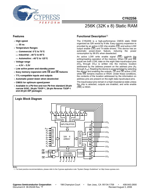
256K (32K x 8) Static RAMCY62256Features•High speed —55ns •Temperature Ranges —Commercial: 0°C to 70°C —Industrial: –40°C to 85°C —Automotive: –40°C to 125°C •Voltage range —4.5V – 5.5V•Low active power and standby power•Easy memory expansion with CE and OE features •TTL-compatible inputs and outputs •Automatic power-down when deselected •CMOS for optimum speed/power•Available in a Pb-free and non Pb-free standard 28-pin narrow SOIC, 28-pin TSOP-1, 28-pin Reverse TSOP-1 and 28-pin DIP packagesFunctional Description [1]The CY62256 is a high-performance CMOS static RAM organized as 32K words by 8 bits. Easy memory expansion is provided by an active LOW chip enable (CE) and active LOW output enable (OE) and Tri-state drivers. This device has an automatic power-down feature, reducing the power consumption by 99.9% when deselected.An active LOW write enable signal (WE) controls the writing/reading operation of the memory. When CE and WE inputs are both LOW, data on the eight data input/output pins (I/O 0 through I/O 7) is written into the memory location addressed by the address present on the address pins (A 0through A 14). Reading the device is accomplished by selecting the device and enabling the outputs, CE and OE active LOW,while WE remains inactive or HIGH. Under these conditions,the contents of the location addressed by the information on address pins are present on the eight data input/output pins.The input/output pins remain in a high-impedance state unless the chip is selected, outputs are enabled, and write enable (WE) is HIGH.Note:1.For best practice recommendations, please refer to the Cypress application note “System Design Guidelines” on .A 9A 8A 7A 6A 5A 4A 3A 2COLUMN DECODERR O W D E C O D E RS E N S E A M P SINPUTBUFFERPOWER DOWNWE OEI/O 0CE I/O 1I/O 2I/O 3I/O 7I/O 6I/O 5I/O 4A 10A 13A 11A 12A A 14A 1Logic Block Diagram32K × 8ARRAYPin ConfigurationsProduct PortfolioProductV CC Range (V)Speed (ns)Power DissipationOperating, I CC(mA)Standby, I SB2(µA)Min.Typ.[2]Max.Typ.[2]Max.Typ.[2]Max.CY62256L Com’l/Ind’l 4.55.05.555/702550250CY62256LL Commercial 7025500.15CY62256LL Industrial 55/7025500.110CY62256LLAutomotive5525500.11512345678910111415162019181721242322Top ViewNarrow SOIC 121325282726GNDA 6A 7A 8A 9A 10A 11A 12A 13WE V CC A 4A 3A 2A 1I/O 7I/O 6I/O 5I/O 4A 14A 5I/O 0I/O 1I/O 2CE OE A 0I/O 322232425262728125101115141312161918173420217689OEA 1A 2A 3A 4WE V CC A 5A 6A 7A 8A 9A 0CE I/O 7I/O 6I/O 5GND I/O 2I/O 1I/O 4I/O 0A 14A 10A 11A 13A 12I/O 3TSOP I Top View (not to scale)Reverse Pinout 22232425262728125101115141312161918173420217689OE A 1A 2A 3A 4WE V CC A 5A 6A 7A 8A 9A 0CE I/O 7I/O 6I/O 5GND I/O 2I/O 1I/O 4I/O 0A 14A 10A 11A 13A 12I/O 3TSOP I Top View (not to scale)12345678910111415162019181721242322Top ViewDIP 121325282726GNDA 6A 7A 8A 9A 10A 11A 12A 13WE V CC A 4A 3A 2A 1I/O 7I/O 6I/O 5I/O 4A 14A 5I/O 0I/O 1I/O 2CE OE A 0I/O 3Pin DefinitionsPin Number Type Description1–10, 21, 23–26Input A 0–A 14. Address Inputs11–13, 15–19, Input/Output I/O 0–/O 7. Data lines. Used as input or output lines depending on operation27Input/Control WE . When selected LOW, a WRITE is conducted. When selected HIGH, a READ is conducted20Input/Control CE . When LOW, selects the chip. When HIGH, deselects the chip22Input/ControlOE . Output Enable. Controls the direction of the I/O pins. When LOW, the I/O pins behave as outputs. When deasserted HIGH, I/O pins are Tri-stated, and act as input data pins14GroundGND . Ground for the device28Power Supply V CC . Power supply for the deviceNote:2.Typical specifications are the mean values measured over a large sample size across normal production process variations and are taken at nominal conditions (T A = 25°C, V CC ). Parameters are guaranteed by design and characterization, and not 100% tested.Maximum Ratings(Above which the useful life may be impaired. For user guide-lines, not tested.)Storage Temperature .................................–65°C to +150°C Ambient Temperature withPower Applied.............................................–55°C to +125°C Supply Voltage to Ground Potential(Pin 28 to Pin 14)..............................................–0.5V to +7V DC Voltage Applied to Outputsin High-Z State[3]....................................–0.5V to V CC + 0.5V DC Input Voltage[3]................................–0.5V to V CC + 0.5V Output Current into Outputs (LOW).............................20 mA Static Discharge Voltage.......................................... > 2001V (per MIL-STD-883, Method 3015)Latch-up Current.................................................... > 200 mA Operating RangeRange Ambient Temperature (T A)[4]V CC Commercial0°C to +70°C 5V± 10% Industrial–40°C to +85°C 5V± 10% Automotive–40°C to +125°C 5V± 10%Electrical Characteristics Over the Operating RangeParameter Description Test ConditionsCY62256−55CY62256−70Unit Min.Typ.[2]Max.Min.Typ.[2]Max.V OH Output HIGH Voltage V CC = Min., I OH = −1.0 mA 2.4 2.4V V OL Output LOW Voltage V CC = Min., I OL = 2.1 mA0.40.4VV IH Input HIGH Voltage 2.2V CC+0.5V 2.2V CC+0.5VVV IL Input LOW Voltage–0.50.8–0.50.8V I IX Input Leakage Current GND < V I < V CC–0.5+0.5–0.5+0.5µA I OZ Output Leakage Current GND < V O < V CC, Output Disabled–0.5+0.5–0.5+0.5µAI CC V CC Operating SupplyCurrent V CC = 5.5V,I OUT = 0 mA,f = f Max = 1/t RCL25502550mALL25502550I SB1Automatic CEPower-down Current—TTL Inputs V CC = 5.5V, CE > V IH,V IN > V IH or V IN < V IL,f = f MaxL0.40.60.40.6mALL0.30.50.30.5I SB2Automatic CEPower-down Current—CMOS Inputs V CC = 5.5V,CE > V CC− 0.3VV IN > V CC− 0.3V, orV IN < 0.3V, f = 0L250250µALL - Com’l0.150.15LL - Ind’l0.1100.110LL - Auto0.115Capacitance[5]Parameter Description Test Conditions Max.UnitC IN Input Capacitance T A = 25°C, f = 1 MHz, V CC = V CC(typ.)6pFC OUT Output Capacitance8pF Thermal Resistance[5]Parameter Description Test Conditions DIP SOIC TSOP RTSOP UnitΘJA Thermal Resistance(Junction to Ambient)Still Air, soldered on a 4.25 x 1.125 inch,2-layer printed circuit board75.6176.5693.8993.89°C/WΘJC Thermal Resistance(Junction to Case)43.1236.0724.6424.64°C/WNotes:3.V IL (min.)= −2.0V for pulse durations of less than 20 ns.4.T A is the “Instant-On” case temperature.5.Tested initially and after any design or process changes that may affect these parameters.AC Test Loads and WaveformsData Retention CharacteristicsParameter DescriptionConditions [6]Min.Typ.[2]Max.Unit V DR V CC for Data Retention 2.0V I CCDRData Retention CurrentL V CC = 2.0V , CE > V CC − 0.3V ,V IN > V CC − 0.3V , or V IN < 0.3V250µA LL - Com’l 0.15µA LL - Ind’l 0.110µA LL - Auto0.110µA t CDR [5]Chip Deselect to Data Retention Time 0ns t R [5]Operation Recovery Timet RCnsData Retention WaveformNote:6.No input may exceed V CC + 0.5V .3.0V 5V OUTPUTR1 1800ΩR2990Ω100pF INCLUDING JIG AND SCOPEGND90%10%90%10%<5ns<5ns5V OUTPUTR1 1800ΩR2990Ω5pFINCLUDING JIG AND SCOPE (a)(b)OUTPUT1.77VEquivalent to:THE VENIN EQUIVALENTALL INPUT PULSES 639ΩV CC(min)V CC(min)t CDRV DR >2V DATA RETENTION MODEt RCEV CCSwitching Characteristics Over the Operating Range[7]Parameter DescriptionCY62256−55CY62256−70Unit Min.Max.Min.Max.Read Cyclet RC Read Cycle Time5570nst AA Address to Data Valid5570nst OHA Data Hold from Address Change55nst ACE CE LOW to Data Valid5570nst DOE OE LOW to Data Valid2535nst LZOE OE LOW to Low-Z[8]55nst HZOE OE HIGH to High-Z[8, 9]2025nst LZCE CE LOW to Low-Z[8]55nst HZCE CE HIGH to High-Z[8, 9]2025nst PU CE LOW to Power-up00nst PD CE HIGH to Power-down5570ns Write Cycle[10, 11]t WC Write Cycle Time5570nst SCE CE LOW to Write End4560nst AW Address Set-up to Write End4560nst HA Address Hold from Write End00nst SA Address Set-up to Write Start00nst PWE WE Pulse Width4050nst SD Data Set-up to Write End2530nst HD Data Hold from Write End00nst HZWE WE LOW to High-Z[8, 9]2025nst LZWE WE HIGH to Low-Z[8]55ns Notes:7.Test conditions assume signal transition time of 5 ns or less, timing reference levels of 1.5V, input pulse levels of 0 to 3.0V, and output loading of the specifiedI OL/I OH and 100 pF load capacitance.8.At any given temperature and voltage condition, t HZCE is less than t LZCE, t HZOE is less than t LZOE, and t HZWE is less than t LZWE for any given device.9.t HZOE, t HZCE, and t HZWE are specified with C L = 5 pF as in (b) of AC Test Loads. Transition is measured ±500 mV from steady-state voltage.10.The internal Write time of the memory is defined by the overlap of CE LOW and WE LOW. Both signals must be LOW to initiate a Write and either signal canterminate a Write by going HIGH. The data input set-up and hold timing should be referenced to the rising edge of the signal that terminates the Write.11.The minimum Write cycle time for Write Cycle #3 (WE controlled, OE LOW) is the sum of t HZWE and t SD.Switching WaveformsRead Cycle No. 1 (Address Transition Controlled)[12, 13]Read Cycle No. 2 (OE Controlled)[13, 14]Write Cycle No. 1 (WE Controlled)[10, 15, 16]Notes:12.Device is continuously selected. OE, CE = V IL .13.WE is HIGH for Read cycle.14.Address valid prior to or coincident with CE transition LOW.15.Data I/O is high impedance if OE = V IH .16.If CE goes HIGH simultaneously with WE HIGH, the output remains in a high-impedance state. 17.During this period, the I/Os are in output state and input signals should not be applied.ADDRESSDATA OUTPREVIOUS DATA VALIDDATA VALIDt RCt AAt OHA50%50%DATA VALIDt RCt ACEt DOEt LZOEt LZCE t PUHIGH IMPEDANCEt HZOE t HZCEt PDIMPEDANCEICCISBHIGH DATA OUTOECEV CC SUPPLY CURRENTt HDt SDt PWEt SAt HAt AWt WCt HZOEDATA IN VALIDNOTE 17DATA I/OADDRESSCEWEOEWrite Cycle No. 2 (CE Controlled)[10, 15, 16]Write Cycle No. 3 (WE Controlled, OE LOW)[11, 16]Switching Waveforms (continued)t WCt AWt SAt HAt HDt SDt SCEDATA IN VALIDWEDATA I/OADDRESSCEt HD t SDt LZWEt SAt HAt AWt WCt HZWEDATA IN VALIDNOTE 17DATA I/OADDRESSWECETypical DC and AC Characteristics1.21.41.00.60.40.24.04.55.05.56.01.61.41.21.00.8−5525125−55251251.21.00.8N O R M A L I Z E D t A A120100806040200.01.02.03.04.0O U T P U T S O U R C E C U R R E N T (m A )SUPPLY VOLTAGE (V)NORMALIZED SUPPLY CURRENT vs.SUPPLY VOLTAGENORMALIZED ACCESS TIME vs.AMBIENT TEMPERATURE AMBIENT TEMPERATURE (°C)NORMALIZED SUPPLY CURRENT vs.AMBIENT TEMPERATUREAMBIENT TEMPERATURE (°C)OUTPUT VOLTAGE (V)OUTPUT SOURCE CURRENT vs.OUTPUT VOLTAGE 0.00.81.41.11.00.94.04.55.05.56.0N O R M A L I Z E D t A ASUPPLY VOLTAGE (V)NORMALIZED ACCESS TIME vs.SUPPLY VOLTAGE 120140*********0.01.02.03.04.0O U T P U T S I N K C U R R E N T (m A )080OUTPUT VOLTAGE (V)OUTPUT SINK CURRENT vs.OUTPUT VOLTAGE0.60.40.20.0N O R M A L I Z E D I C CN O R M A L I Z E D I C C , I S BI CCI CCV CC = 5.0VV CC = 5.0V T A = 25°CV CC = 5.0V T A = 25°CI SBT A = 25°C0.60.801.31.2V IN = 5.0V T A = 25°C1.4V CC = 5.0V V IN = 5.0V−55251052.52.01.5CURRENT vs.AMBIENT TEMPERATUREAMBIENT TEMPERATURE (°C)1.00.50.0–0.5I SB3.0STANDBY V CC = 5.0V V IN = 5.0VI S B 2 µATruth TableCE WE OE Inputs/Outputs ModePowerH X X High-Z Deselect/Power-down Standby (I SB )L H L Data Out Read Active (I CC )L L X Data In WriteActive (I CC )LHHHigh-ZOutput DisabledActive (I CC )Typical DC and AC Characteristics (continued)3.02.52.01.51.00.50.01.02.03.04.0N O R M A L I Z E D I P OSUPPLY VOLTAGE (V)TYPICAL POWER-ON CURRENT vs.SUPPLY VOLTAGE 30.025.020.015.010.05.00200400600800D E L T A t (n s )AA CAPACITANCE (pF)TYPICAL ACCESS TIME CHANGE vs.OUTPUT LOADING1.251.000.7510203040N O R M A L I Z E D I C CCYCLE FREQUENCY (MHz)0.05.00.010000.50V CC = 4.5V T A = 25°CV CC =5.0V T A = 2 5°C V IN = 0.5VNORMALIZED I CC vs. CYCLE TIMEOrdering InformationSpeed(ns)Ordering Code PackageDiagram Package TypeOperatingRange55CY62256LL−55SNI51-8509228-pin (300-mil Narrow Body) SNC Industrial CY62256LL−55SNXI28-pin (300-mil Narrow Body) SNC (Pb-free)CY62256LL−55ZXI51-8507128-pin TSOP I (Pb-free)CY62256LL−55SNE51-8509228-pin (300-mil Narrow Body) SNC AutomotiveCY62256LL−55SNXE28-pin (300-mil Narrow Body) SNC (Pb-free)CY62256LL−55ZE51-8507128-pin TSOP ICY62256LL−55ZXE28-pin TSOP I (Pb-free)CY62256LL−55ZRXE51-8507428-pin Reverse TSOP I (Pb-free)70CY62256LL−70PC51-8501728-pin (600-Mil) Molded DIP Commercial CY62256LL−70PXC28-pin (600-Mil) Molded DIP (Pb-free)CY62256L−70SNC51-8509228-pin (300-mil Narrow Body) SNCCY62256L−70SNXC28-pin (300-mil Narrow Body) SNC (Pb-free)CY62256LL−70SNC28-pin (300-mil Narrow Body) SNCCY62256LL−70SNXC28-pin (300-mil Narrow Body) SNC (Pb-free)CY62256LL−70ZC51-8507128-pin TSOP ICY62256LL−70ZXC28-pin TSOP I (Pb-free)CY62256L–70SNI51-8509228-pin (300-mil Narrow Body) SNC IndustrialCY62256L–70SNXI28-pin (300-mil Narrow Body) SNC (Pb-free)CY62256LL−70SNI28-pin (300-mil Narrow Body) SNCCY62256LL−70SNXI28-pin (300-mil Narrow Body) SNC (Pb-free)CY62256LL−70ZXI51-8507128-pin TSOP I (Pb-free)CY62256LL−70ZRI51-8507428-pin Reverse TSOP ICY62256LL−70ZRXI28-pin Reverse TSOP I (Pb-free)Please contact your local Cypress sales representative for availability of these partsPackage DiagramsPackage Diagrams (continued)28-pin Thin Small Outline Package Type 1 (8 x 13.4 mm) (51-85071)51-85071-*GDocument #: 38-05248 Rev. *F Page 13 of 14All product and company names mentioned in this document are the trademarks of their respective holders.Package Diagrams (continued)51-85074-*F28-pin Reverse Thin Small Outline Package Type 1 (8x13.4 mm) (51-85074)Document History PageDocument Title: CY62256, 256K (32K x 8) Static RAM Document Number: 38-05248REV.ECN NO.IssueDateOrig. ofChange Description of Change**11345403/06/02MGN Change from Spec number: 38-00455 to 38-05248Remove obsolete parts from ordering info, standardize format*A11522705/23/02GBI Changed SN Package Diagram*B11650609/04/02GBI Added footnote 1Corrected package description in Ordering Information table*C238448See ECN AJU Added Automotive product information*D344595See ECN SYT Added Pb-free packages on page# 10*E395936See ECN SYT Changed address of Cypress Semiconductor Corporation on Page# 1 from“3901 North First Street” to “198 Champion Court”Added CY62256L–70SNXI package in the Ordering Information on Page # 10 *F493277See ECN VKN Updated Ordering Information table。
HM62256BLFP-10T中文资料
The Hitachi HM62256B is a CMOS static RAM organized 32-kword ×8-bit. It realizes higher performance and low power consumption by employing 0.8 µm Hi-CMOS process technology. The device, packaged in 8 ×14 mm TSOP, 8 ×13.4 mm TSOP with thickness of 1.2 mm, 450-mil SOP (foot print pitch width), 600-mil plastic DIP, or 300-mil plastic DIP, is available for high density mounting. It offers low power standby power dissipation; therefore, it is suitable for battery back-up systems.Features•High speedFast access time: 70/85/100/120 ns (max)•Low powerStandby: 1.5 µW (typ)Operation: 25 mW (typ) (f = 1 MHz)•Single 5 V supply•Completely static memoryNo clock or timing strobe required•Equal access and cycle times•Common data input and outputThree state output•Directly TTL compatibleAll inputs and outputs•Capability of battery back up operation Ordering InformationType No.Access time Package ————————————————————–HM62256BLP-770 ns600-milHM62256BLP-885 ns28-pinHM62256BLP-10100 ns plastic DIPHM62256BLP-12120 ns(DP-28)—————————————HM62256BLP-7SL70 nsHM62256BLP-8SL85 nsHM62256BLP-10SL100 nsHM62256BLP-12SL120 ns ————————————————————–HM62256BLSP-770 ns300-milHM62256BLSP-885 ns28-pinHM62256BLSP-10100 ns plastic DIPHM62256BLSP-12120 ns(DP-28NA)—————————————HM62256BLSP-7SL70 nsHM62256BLSP-8SL85 nsHM62256BLSP-10SL100 nsHM62256BLSP-12SL120 ns ————————————————————–HM62256BLFP-7T70 ns450-milHM62256BLFP-8T85 ns28-pinHM62256BLFP-10T100 ns plastic SOPHM62256BLFP-12T120 ns(FP-28DA)—————————————HM62256BLFP-7SLT70 nsHM62256BLFP-8SLT85 nsHM62256BLFP-10SLT100 nsHM62256BLFP-12SLT120 ns ————————————————————–HM62256BLT-885 ns8 mm ×14 mm HM62256BLT-10100 ns32-pin TSOP HM62256BLT-12120 ns(TFP-32DA)—————————————HM62256BLT-7SL70 nsHM62256BLT-8SL85 ns ————————————————————–HM62256BLTM-885 ns8 mm ×13.4 mm —————————————28-pin TSOP HM62256BLTM-7SL70 ns(TFP-28DA) HM62256BLTM-8SL85 ns ————————————————————HM62256B Series32,768-word × 8-bit High Speed CMOS Static RAMPin ArrangementPin DescriptionSymbol Function ————————————————————A0 – A14Address ————————————————————I/O0 – I/O7Input/output ————————————————————CS Chip select ————————————————————WE Write enable ————————————————————Symbol Function ————————————————————OE Output enable ————————————————————NC No connection ————————————————————V CC Power supply ————————————————————V SS Ground ————————————————————Block DiagramFunction TableWE CS OE Mode V CC current I/O pin Ref. cycle ———————————————————————————————————————————X H X Not selected I SB, I SB1High-Z————————————————————————————————————————————H L H Output disable I CC High-Z————————————————————————————————————————————H L L Read I CC Dout Read cycle (1)–(3)———————————————————————————————————————————L L H Write I CC Din Write cycle (1)———————————————————————————————————————————L L L Write I CC Din Write cycle (2)———————————————————————————————————————————Note:X: H or LAbsolute Maximum RatingsParameter Symbol Value Unit ———————————————————————————————————————————Power supply voltage*1V CC–0.5 to +7.0V ———————————————————————————————————————————Terminal voltage*1V T–0.5*2to V CC + 0.3*3V ———————————————————————————————————————————Power dissipation P T 1.0W ———————————————————————————————————————————Operating temperature Topr0 to + 70°C ———————————————————————————————————————————Storage temperature Tstg–55 to +125°C ———————————————————————————————————————————Storage temperature under bias Tbias–10 to +85°C ———————————————————————————————————————————Note: 1.Relative to V SS2.V T min: –3.0 V for pulse half-width ≤50 ns3.Maximum voltage is 7.0 VRecommended DC Operating Conditions (Ta = 0 to +70°C)Parameter Symbol Min Typ Max Unit ———————————————————————————————————————————Supply voltage V CC 4.5 5.0 5.5V———————————————————————————————V SS000V ———————————————————————————————————————————Input high (logic 1) voltage V IH 2.2—V CC+0.3V ———————————————————————————————————————————Input low (logic 0) voltage V IL–0.5 *1—0.8V ———————————————————————————————————————————Note: 1.V IL min: –3.0 V for pulse half-width ≤50 nsWrite CycleHM62256B-7HM62256B-8HM62256B-10HM62256B-12————————–————–————–Parameter Symbol Min Max Min Max Min Max Min Max Unit Notes ——————————————————————————————————————————Write cycle time t WC70—85—100—120—ns ——————————————————————————————————————————Chip selection to t CW60—75—80—85—ns2end of write ——————————————————————————————————————————Address setup time t AS0—0—0—0—ns3——————————————————————————————————————————Address valid to t AW60—75—80—85—nsend of write ——————————————————————————————————————————Write pulse width t WP50—55—60—70—ns1, 12——————————————————————————————————————————Write recovery time t WR0—0—0—0—ns4——————————————————————————————————————————WE to output in high-Z t WHZ025030035 040 ns10,11——————————————————————————————————————————Data to write time overlap t DW30—35—40—50—ns ——————————————————————————————————————————Data hold from write time t DH0—0—0—0—ns ——————————————————————————————————————————Output active from t OW5—5—5—5—ns10end of write ——————————————————————————————————————————Output disable to output t OHZ025*********ns10, 11in high-Z ——————————————————————————————————————————Write Timing Waveform (2) (OE Low Fixed)*12Notes: 1.Typical values are at V CC = 3.0 V , Ta = 25°C and not guaranteed.2. 10 µA max at Ta = 0 to + 40˚C.3.3 µA max at Ta = 0 to + 40˚C. (only for L-SL version)4.t RC = read cycle time.5.CS controls address buffer, WE buffer, OE buffer, and Din buffer. If CS controls data retention mode, Vin levels (address, WE , OE , I/O) can be in the high impedance state.11HM62256B SeriesHM62256B Series。
实验二RAM扩展实验[资料]
![实验二RAM扩展实验[资料]](https://img.taocdn.com/s3/m/712ec6c1185f312b3169a45177232f60ddcce718.png)
实验二RAM扩展实验(请在实验课前写好预习报告,预习报告日期必在做实验课之前,预习报告中应该出现跟实验1内容相关的原理,电路图(可简画),流程图(或是程序,有程序就必带注释))实验仪器:pc机,8086k微机原理实验箱实验目的:1.掌握存储器芯片的特性及与CPU的连接方法。
2.掌握访问连续存储空间的方法。
注意实验报告中3个内容每人都要做,1通过实验课前仿真实验完成,2,3是实验课时完成。
每个具体实验内容包括:写出电路图,连线,流程图,程序(必须在关键地方加上注释),实验结果,问题分析和每个实验内容中的思考题。
0实验内容:(1必须在实验课前通过仿真实验完成,电路为EX2_1.DSN,程序为EX2_1.ASM)1.利用62256(32K×8bit)的静态SRAM芯片进行扩展,要求扩展的存储器容量为64KB,且要求和8086CPU相连接。
扩展后,利用此扩展的存储体进行读写访问,将内存0000H:4000H 地址开始的位置至0000H:4063H位置处依次写上0-99。
实验连线:提示:应该有哪三类线?实验流程图参考实验程序:assume cs:codecode segmentstart:mov ax,0000h ;设置DS的段地址值为0mov ds,axmov bx,4000H ;利用BX存放存储单元的偏移地址,从200H开始mov al,0 ;AL中为要写到存储单元中的数据。
初始值为1mov ds:[bx],al ;将1写入内存0000H:4000H地址处mov cx,100 ;设置循环次数为100次l1:mov ds:[bx],al ;循环体目的将AL中的值填入存储器inc bx ;偏移地址指针下移一个字节inc al ;待填充到存储单元的数据也自增1loop l1 ;根据CX的次数执行上面的循环体int 3 ;断点中断,目的是为了观察内存结果,用实验箱做实验时,不用这步code endsend start提示:如果仿真过程中把内存窗口关掉,可以按图中所示选择调试菜单中:即可出现思考问题:1)通过EX2_1.DSN仿真运行结果观察两块62256芯片写入的内容各有什么特点?为什么会产生这样的结果?2)停止运行,观察EX2_1.DSN仿真图,U7:62256芯片的片选段CE由那两个信号进行或运算获得?这两个信号都为哪种电平时才能选中这块U7:62256芯片。
人脸识别系统

鉴别人的身份是一个非常困难的问题,传统的身份鉴别方法把这个问题转化为鉴别一些标识个人身份的事物,这包括两个方面:①身份标识物品,比如钥匙、证件、ATM 卡等;②身份标识知识,比如用户名和密码。
在一些安全性要求严格的系统中,可以将这两者结合起来,比如ATM 机要求用户同时提供ATM 卡和密码。
这些传统的身份鉴别方法存在明显的缺点:个人拥有的物品容易丢失或被伪造,个人的密码容易遗忘或记错。
更为严重的是这些系统无法区分真正的拥有者和取得身份标识物的冒充者,一旦他人获得了这些身份标识事物,就可以拥有相同针对这一情况,我们可以采取两种措施加以解决。
其一,研究新的适用于非完全正立人脸图像的特征检测方法并对人脸特征的提取作相应的调整,这种解决方法在文献[9]已有所尝试;其二,沿用现有的人脸识别系统,但在人脸图像送识别系统进行特征提取和识别之前(即在人脸检测和定位阶段),先进行人脸位置矫正的工作,这种方法在文献[10]中也已有所研究,并取得了较好的效果。
与传统的身份鉴定手段相比,基于人脸生物特征信息的身份鉴定技术具有以下优点:● 用户易接受:简单易用,对用户无特殊要求。
● 防伪性能好:不易伪造或被盗。
● “随身携带”:不用担心遗漏或丢失,随时随地可用。
除此之外,人脸识别技术还有主动性好,精确性高,性能/成本比高,自学习功能强等优点。
河北工程大学毕业论文鉴于人脸识别技术在个人身份鉴定方面的众多优点,这项技术可以在很多领域得到应用:● 国家安全领域。
协助公安,海关等国家安全机构加强对可疑人物、罪犯、恐怖分子的追踪、监控和识别。
● 公众安全领域。
加强交通管制;确认身份证、护照等证件的真伪;验证各类信用卡的持卡人身份。
●计算机交互领域。
根据计算机使用者人脸特征确定身份,提供个性化服务。
Face Pose Adjustment, Facial Feature Extraction , Human Face Recognition , 人脸识别技术在这些领域的充分利用,对于有效地鉴定个人的身份,防止犯罪和诈骗、提高办公效率、节约资源有着重大的社会和经济意义。
了解电脑内存(RAM)的工作原理与选购建议

了解电脑内存(RAM)的工作原理与选购建议电脑内存(Random Access Memory,RAM)是计算机系统中重要的组件之一。
它承担着临时存储和处理数据的任务,对于计算机的性能和运行速度起着至关重要的作用。
本文将介绍RAM的工作原理,并提供选购RAM的建议。
一、RAM的工作原理RAM是计算机中的主要存储介质之一,它位于计算机主板上,并且是以芯片的形式进行组织。
RAM可以快速读取和写入数据,与计算机的中央处理器(CPU)之间通过内存总线进行通信。
RAM的主要工作原理是根据CPU的指令,将数据从存储介质(如硬盘)中读取到RAM中供CPU处理。
RAM通过内存控制器将数据传递给CPU,并将处理结果写回RAM或其他存储介质中。
RAM的工作速度非常快,它的响应时间一般在纳秒级别,远远快于传统的存储介质。
这使得RAM成为计算机在运行过程中临时存储和处理数据的重要组件。
二、选购RAM的建议1. 确定RAM的容量需求RAM的容量决定了计算机可以同时存储和处理的数据量。
对于一般的办公和网页浏览应用,通常8GB至16GB的RAM已经足够。
而对于需要运行大型软件、进行高性能游戏或进行专业图形设计等需求较高的用户,则可以选择16GB以上的RAM容量。
2. 确定RAM的类型和频率RAM有多种类型,包括DDR3、DDR4等,而每种类型又有不同的频率。
在选择RAM时,需要根据自己计算机主板支持的类型和频率来确定。
一般来说,较新的主板通常支持DDR4,并且更高的频率能够提供更快的数据读取和写入速度。
3. 考虑RAM的时序和延迟RAM的时序和延迟也是选择RAM时需要考虑的因素。
时序和延迟反映了RAM芯片内部数据传输的速度和效率。
通常来说,时序越低、延迟越短,RAM的性能越好。
因此,在选购RAM时,可以选择具有较低时序和延迟的产品。
4. 预留空间用于未来升级在选购RAM时,可以预留一定的空间用于未来的升级。
考虑到计算机技术的不断发展和软件需求的增加,留下一定的扩展余地可以在以后需要升级时避免再次购买新的RAM。
62256ram

© 1990, 1993, 1994µPD43256B256K-BIT CMOS STATIC RAM32K-WORD BY 8-BITDescriptionThe µPD43256B is a high speed, low power, and 262, 144 bits (32,768 words by 8 bits) CMOS static RAM.Battery backup is available (L, LL, A, and B versions). And A and B versions are wide voltage operations.The µPD43256B is packed in 28-pin plastic DIP, 28-pin plastic SOP and 28-pin plastic TSOP (I).Features•32,768 words by 8 bits organization•Fast access time: 70, 85, 100, 120, 150 ns (MAX.)•Wide voltage range (A version: V CC = 3.0 to 5.5 V, B version: V CC = 2.7 to 5.5 V)• 2 V data retention•OE input for easy applicationAccess time Operating Operating Standby Data retention Part numberns (MAX.)supply voltagetemperaturesupply currentsupply current Note 1V °C µA (MAX.)µA (MAX.)µPD43256B-L 70, 85 4.5 to 5.50 to 70503µPD43256B-LL 70, 85152µPD43256B-A 85, 100Note 2, 120Note 23.0 to 5.5µPD43256B-B Note 2100, 120, 1502.7 to 5.5Notes 1.T A ≤ 40 ˚C, V CC = 3 V2.Access time : 85 ns (MAX.) (V CC = 4.5 to 5.5 V)Version X and PThis data sheet can be applied to the version X and P. Each version is identified with its lot number. Letter X in the fifth character position in a lot number signifies version X, letter P, version P.The information in this document is subject to change without notice.The mark shows major revised points.Document No. M10770EJ9V0DS00 (9th edition)Date Published May 1997 N Printed in JapanLot number2Ordering InformationAccess time Operating Operating Part number Package ns (MAX.)supply voltagetemperatureRemark V ˚C µPD43256BCZ-70L 28-pin plastic 70 4.5 to 5.50 to 70L VersionµPD43256BCZ-85L DIP (600 mil)85µPD43256BCZ-70LL 70LL VersionµPD43256BCZ-85LL 85µPD43256BGU-70L 28-pin plastic 70L VersionµPD43256BGU-85L SOP (450 mil)85µPD43256BGU-70LL 70LL VersionµPD43256BGU-85LL 85µPD43256BGU-A8585 3.0 to 5.5A VersionµPD43256BGU-A10100µPD43256BGU-A12120µPD43256BGU-B10100 2.7 to 5.5 B VersionµPD43256BGU-B12120µPD43256BGU-B15150µPD43256BGW-70LL-9JL 28-pin plastic 70 4.5 to 5.5LL VersionµPD43256BGW-85LL-9JL TSOP (I)85µPD43256BGW-A85-9JL (8 × 13.4 mm)85 3.0 to 5.5 A VersionµPD43256BGW-A10-9JL (Normal bent)100µPD43256BGW-A12-9JL 120µPD43256BGW-B10-9JL 100 2.7 to 5.5 B VersionµPD43256BGW-B12-9JL 120µPD43256BGW-B15-9JL 150µPD43256BGW-70LL-9KL 28-pin plastic 70 4.5 to 5.5LL VersionµPD43256BGW-85LL-9KL TSOP (I)85µPD43256BGW-A85-9KL (8 × 13.4 mm)85 3.0 to 5.5 A VersionµPD43256BGW-A10-9KL (Reverse bent)100µPD43256BGW-A12-9KL 120µPD43256BGW-B10-9KL 100 2.7 to 5.5 B VersionµPD43256BGW-B12-9KL 120µPD43256BGW-B15-9KL1503Pin Configuration (Marking Side)A14 A12 A7 A6 A5 A4 A3 A2 A1 A0 I/O1 I/O2 I/O3 GND28-pin plastic DIP (600 mil) PD43256BCZ 28-pin plastic SOP (450 mil) PD43256BGUµµA0 - A14:Address inputs I/O1 - I/O8:Data inputs/outputsCS :Chip Select WE :Write Enable OE :Output Enable V CC :Power supply GND:Ground428-pin plastic TSOP (I) (8 × 13.4 mm) (Normal bent)PD43256BGW-9JLµA10CS I/O8I/O7I/O6I/O5I/O4GND I/O3I/O2I/O1A0A1A2OE A11A9A8A13WE V CC A14A12A7A6A5A4A328-pin plastic TSOP (I) (8 × 13.4 mm) (Reverse bent)PD43256BGW-9KLµA10CS I/O8I/O7I/O6I/O5I/O4GND I/O3I/O2I/O1A0A1A2OE A11A9A8A13WE V CC A14A12A7A6A5A4A3Block DiagramCSOEV CCGNDTruth TableCS OE WE Mode I/O Supply currentH××Not selected High impedance I SBL H H Output disable I CCAL×L Write D INL L H Read D OUTRemark×: Don’t care5Electrical CharacteristicsAbsolute Maximum RatingsParameter Symbol Rating Unit Supply voltage V CC–0.5Note to +7.0V Input/Output voltage V T–0.5Note to V CC + 0.5V Operating ambient temperature T A0 to 70˚C Storage temperature T stg–55 to +125˚CNote –3.0 V (MIN.) (Pulse width 50 ns)Caution Exposing the device to stress above those listed in absolute maximum ratings could cause permanent damage. The device is not meant to be operated under conditions outside thelimits described in the operational sections of this characteristics. Exposure to absolutemaximum rating conditions for extended periods may affect device reliability. Recommended Operating ConditionsParameter Symbol µPD43256B-LµPD43256B-AµPD43256B-BUnit µPD43256B-LLMIN.MAX.MIN.MAX.MIN.MAX.Supply voltage V CC 4.5 5.5 3.0 5.5 2.7 5.5V High level input voltage V IH 2.2V CC + 0.5 2.2V CC + 0.5 2.2V CC + 0.5V Low level input voltage V IL–0.3Note+0.8–0.3Note+0.5–0.3Note+0.5V Operating ambient temperature T A070070070˚CNote –3.0 V (MIN.) (Pulse width 50 ns)6DC Characteristics (Recommended operating conditions unless otherwise noted) (1/2)Parameter Symbol Test conditionsµPD43256B-LµPD43256B-LLUnit MIN.TYP.MAX.MIN.TYP.MAX.Input leakage current I LI V IN = 0 V to V CC–1.0+1.0–1.0+1.0µAI/O leakage current I LO V I/O = 0 V to V CC–1.0+1.0–1.0+1.0µAOE = V IH or CS = V IH or WE = V ILOperating supply current I CCA1CS = V IL, Minimum cycle time,4545mAI I/O = 0 mAI CCA2CS = V IL, I I/O = 0 mA1010I CCA3CS ≤ 0.2 V, Cycle = 1 MHz,1010I I/O = 0 mAV IL≤ 0.2 V, V IH≥ V CC – 0.2 VStandby supply current I SB CS = V IH33mAI SB1CS ≥ V CC – 0.2 V 1.0500.515µA High level output voltage V OH1I OH = –1.0 mA 2.4 2.4VV OH2I OH = –0.1 mA V CC–0.5V CC–0.5Low level output voltage V OL I OL = 2.1 mA0.40.4VRemarks 1.V IN: Input voltage2.These DC Characteristics are in common regardless of package types.7DC Characteristics (Recommended operating conditions unless otherwise noted) (2/2)Parameter Symbol Test conditionsµPD43256B-AµPD43256B-BUnit MIN.TYP.MAX.MIN.TYP.MAX.Input leakage current I LI V IN = 0 V to V CC–1.0+1.0–1.0+1.0µAI/O leakage current I LO V I/O = 0 V to V CC–1.0+1.0–1.0+1.0µACS = V IH or WE = V IL or OE = V IHOperating supply current I CCA1CS = V IL,µPD43256B-A8545—mAMinimum cycle time,µPD43256B-A10I I/O = 0 mAµPD43256B-A12µPD43256B-B10—45µPD43256B-B12µPD43256B-B15V CC≤ 3.3 V—20I CCA2CS = V IL, I I/O = 0 mA1010V CC≤ 3.3 V—5I CCA3CS ≤ 0.2 V, Cycle = 1 MHz,1010I I/O = 0 mA,V IL≤ 0.2 V,V IH≥ V CC – 0.2 V VCC≤ 3.3 V—5Standby supply current I SB CS = V IH33mAV CC≤ 3.3 V—2I SB1CS ≥ V CC – 0.2 V0.5150.515µAV CC≤ 3.3 V—0.510High level output voltage V OH1I OH = –1.0 mA, V CC≥ 4.5 V 2.4 2.4VI OH = –0.5 mA, V CC < 4.5 V 2.4 2.4V OH2I OH = –0.1 mA——I OH = –0.02 mA V CC–0.1V CC–0.1Low level output voltage V OL I OL = 2.1 mA, V CC≥ 4.5 V0.40.4VI OL = 1.0 mA, V CC < 4.5 V0.40.4V OL1I OL = 0.02 mA0.10.1 Remarks 1.V IN: Input voltage2.These DC characteristics are in common regardless of package types.Capacitance (T A = 25 ˚C, f = 1 MHz)Parameter Symbol Test conditions MIN.TYP.MAX.Unit Input capacitance C IN V IN = 0 V5pF Input/Output capacitance C I/O V I/O = 0 V8pF Remarks 1.V IN: Input voltage2.These parameters are periodically sampled and not 100 % tested.8AC Characteristics (Recommended operating conditions unless otherwise noted) AC Test ConditionsInput waveform (Rise/fall time ≤ 5 ns)Input pulse levels0.8 V to 2.2 V: µPD43256B-L, 43256B-LL0.5 V to 2.2 V: µPD43256B-A, 43256B-BOutput waveformOutput loadµPD43256B-A, 43256B-B : 1TTL + 100 pFµPD43256B-L, 43256B-LL:AC characteristics with notes should be measured with the output load shown inFigure 1 and Figure 2.Figure 1Figure 2(For t AA, t ACS, t OE, t OH)(For t CHZ, t CLZ, t OHZ, t OLZ, t WHZ, t OW)I/O (Output)Ω100 pFC LI/O (Output)Ω5 pFC LRemark C L includes capacitances of the probe and jig, and stray capacitances.910Read Cycle (1/2)V CC ≥ 4.5 VµPD43256B-85ParameterSymbolµPD43256B-70µPD43256B-A85/A10/A12Unit ConditionµPD43256B-B10/B12/B15MIN.MAX.MIN.MAX.Read cycle time t RC 7085nsAddress access time t AA 7085ns Note 1CS access time t ACS 7085ns OE access timet OE 3540ns Output hold from address change t OH 1010ns CS to output in low impedance t CLZ 1010ns Note 2OE to output in low impedance t OLZ 55nsCS to output in high impedance t CHZ 3030ns OE to output in high impedancet OHZ3030nsNotes 1.See the output load shown in Figure 1 except for µPD43256B-A, 43256B-B.2.See the output load shown in Figure 2 except for µPD43256B-A, 43256B-B.Remark These AC characteristics are in common regardless of package types and L, LL versions.Read Cycle (2/2)VCC ≥ 3.0 VV CC ≥ 2.7 VParameterSymbol µPD43256B-A85 µPD43256B-A10µPD43256B-A12µPD43256B-B10µPD43256B-B12µPD43256B-B15UnitMIN.MAX.MIN.MAX.MIN.MAX.MIN.MAX.MIN.MAX.MIN.MAX.Read cycle time t RC 85100120100120150ns Address access time t AA 85100120100120150ns Note CS access time t ACS 85100120100120150ns OE access timet OE 506060606070ns Output hold from address change t OH 101010101010ns CS to output in low impedance t CLZ 101010101010ns OE to output in low impedance t OLZ 555555ns CS to output in high impedance t CHZ 353540354050ns OE to output in high impedancet OHZ353540354050nsNote Loading condition is 1TTL + 100 pF.Remark These AC characteristics are in common regardless of package types and L, LL versions.Con-ditionRead Cycle Timing ChartRemark In read cycle, WE should be fixed to high level.Address (Input)CS (Input)OE (Input)I/O (Output)Write Cycle (1/2)V CC ≥ 4.5 VµPD43256B-85ParameterSymbolµPD43256B-70µPD43256B-A85/A10/A12Unit ConditionµPD43256B-B10/B12/B15MIN.MAX.MIN.MAX.Write cycle time t WC 7085ns CS to end of writet CW 5070ns Address valid to end of write t AW 5070ns Write pulse width t WP 5560ns Data valid to end of write t DW 3035ns Data hold time t DH 00ns Address setup time t AS 00ns Write recovery timet WR 0nsWE to output in high impedance t WHZ 3030ns NoteOutput active from end of writet OW1010nsNote See the output load shown in Figure 2 except for µPD43256B-A, 43256B-B.Remark These AC characteristics are in common regardless of package types and L, LL versions.Write Cycle (2/2)V CC ≥ 3.0 VV CC ≥ 2.7 VParameterSymbol µPD43256B-A85 µPD43256B-A10µPD43256B-A12µPD43256B-B10µPD43256B-B12µPD43256B-B15UnitMIN.MAX.MIN.MAX.MIN.MAX.MIN.MAX.MIN.MAX.MIN.MAX.Write cycle time t WC 85100120100120150ns CS to end of writet CW 7070907090100ns Address valid to end of write t AW 7070907090100ns Write pulse width t WP 606080608090ns Data valid to end of write t DW 606070607080ns Data hold time t DH 000000ns Address setup time t AS 000000ns Write recovery timet WR 0ns WE to output in high impedance t WHZ 303540354050ns Note Output active from end of writet OW101010101010nsNote Loading condition is 1TTL + 100 pF.Remark These AC characteristics are in common regardless of package types and L, LL versions.Con-ditionWrite Cycle Timing Chart 1 (WE Controlled)Address (Input)WE (Input)I/O (Input/Output)Cautions 1.CS or WE should be fixed to high level during address transition.2.When I/O pins are in the output state, do not apply to the I/O pins signals that are oppositein phase with output signals.Remarks1.Write operation is done during the overlap time of a low level CS and a low level WE.2.When WE is at low level, the I/O pins are always high impedance. When WE is at high level,read operation is executed. Therefore OE should be at high level to make the I/O pins highimpedance.3.If CS changes to low level at the same time or after the change of WE to low level, the I/O pinswill remain high impedance state.Write Cycle Timing Chart 2 (CS Controlled)Address (Input)CS (Input)WE (Input)I/O (Input)Cautions 1.CS or WE should be fixed to high level during address transition.2.When I/O pins are in the output state, do not apply to the I/O pins signals that are oppositein phase with output signals.Remark Write operation is done during the overlap time of a low level CS and a low level WE.Low V CC Data Retention CharacteristicsL Version (µPD43256B-L: T A = 0 to 70 ˚C)Parameter Symbol Test conditions MIN.TYP.MAX.Unit Data retention supply voltage V CCDR CS ≥ V CC – 0.2 V 2.0 5.5V Data retention supply current I CCDR V CC = 3.0 V, CS ≥ V CC – 0.2 V0.520NoteµAChip deselection to data t CDR0ns retention modeOperation recovery time t R5ms Note 3 µA (T A≤ 40 ˚C)LL Version (µPD43256B-LL: T A = 0 to 70 ˚C)A Version (µPD43256B-A: T A = 0 to 70 ˚C)B Version (µPD43256B-B: T A = 0 to 70 ˚C)Parameter Symbol Test conditions MIN.TYP.MAX.Unit Data retention supply voltage V CCDR CS ≥ V CC – 0.2 V 2.0 5.5V Data retention supply current I CCDR V CC = 3.0 V, CS ≥ V CC – 0.2 V0.57NoteµAChip deselection to data t CDR0ns retention modeOperation recovery time t R5ms Note 2 µA (T A≤ 40 ˚C), 1 µA (T A≤ 25 ˚C)Data Retention Timing Chart5.0 V4.5 VV IH (MIN.)V CCDRV IL (MAX.)GNDNote A Version: 3.0 V, B Version: 2.7 VRemark The other pins (address, OE, WE, I/Os) can be in high impedance state.Package Drawings28 PIN PLASTIC DIP (600 mil)ITEM MILLIMETERS INCHES A B C F G H I J K 38.10 MAX. 2.54 (T.P.) 3.6±0.3 0.51 MIN. 4.31 MAX. 2.54 MAX. L 0.25 15.24 (T.P.) 5.72 MAX. 13.2 N 1.2 MIN. 1.500 MAX. 0.100 MAX. 0.047 MIN. 0.142±0.012 0.020 MIN. 0.170 MAX. 0.226 MAX. 0.600 (T.P.) 0.5200.01 0.100 (T.P.)P28C-100-600A1-1D 0.50±0.10 0.020 M 0.25 0.010 +0.10 –0.05 R0 ~ 15°0 ~ 15°+0.004–0.005 +0.004 –0.003 NOTESEach lead centerline is located within 0.25 mm (0.01 inch) of its true position (T.P.) at maximum material condition. Item "K" to center of leads when formed parallel.1) 2)P NOTEEach lead centerline is located within 0.12 mm (0.005 inch) of its true position (T.P.) at maximum material condition.28 PIN PLASTIC SOP (450 mil)P28GU-50-450A-1ITEM MILLIMETERS INCHES A B C D E F G H I J 19.05 MAX. 1.27 (T.P.) 3.0 MAX. 2.55±0.1 11.8±0.3 1.27 MAX. K L 0.12 0.7±0.2 1.7±0.2 8.4±0.1 0.20 M 0.10 0.40±0.10 0.2±0.1 N +0.07 –0.03 0.750 MAX. 0.050 MAX. 0.016 0.008±0.004 0.119 MAX. 0.100 0.465 0.331 0.067±0.008 0.008 0.028 0.005 0.004 +0.008 –0.009 0.050 (T.P.) P5°±5°5°±5°+0.004 –0.005 +0.005–0.004 +0.012 –0.013 +0.004 –0.005 +0.003 –0.002 detail of lead end28PIN PLASTIC TSOP ( I ) (8×13.4)ITEM MILLIMETERS INCHESNOTE(1) Each lead centerline is located within 0.08 mm (0.003 inch) of its true position (T.P.) at maximum material condition. P28GW-55-9JL-1M 0.08 0.003 N 0.10 0.004 H 12.4±0.2 0.488±0.008 I 11.8±0.1 0.465 +0.004 –0.005 J 0.8±0.2 0.031 +0.009 –0.008S1.2 MAX.0.048 MAX. A 8.0±0.1 0.315±0.004 B 0.6 MAX. 0.024 MAX. C 0.55 (T.P.)0.022 (T.P.)G 1.0 0.039 K 0.145 0.006±0.001 L 0.5±0.1 0.020 +0.004 –0.005 P 13.4±0.2 0.528 +0.008 –0.009 Q 0.1±0.050.004±0.002 R 3° +7° –3° 3° +7° –3° D 0.22 0.009±0.003 +0.08 –0.07detail of lead end +0.025 –0.015 1 14 2815(2) "A" excludes mold flash. (Includes mold flash : 8.4mm MAX. <0.331 inch MAX.>)28PIN PLASTIC TSOP ( I ) (8×13.4)ITEM MILLIMETERS INCHESNOTEP28GW-55-9KL-1M 0.08 0.003 N 0.10 0.004 H 12.4±0.2 0.488±0.008 I 11.8±0.1 0.465 +0.004 –0.005 J 0.8±0.2 0.031 +0.009 –0.008S1.2 MAX.0.048 MAX. A 8.0±0.1 0.315±0.004 B 0.6 MAX. 0.024 MAX. C 0.55 (T.P.)0.022 (T.P.)G 1.0 0.039 K 0.145 0.006±0.001 L 0.5±0.1 0.020 +0.004 –0.005 P 13.4±0.2 0.528 +0.008 –0.009 Q 0.1±0.050.004±0.002 R 3° +7° –3° 3° +7° –3° D 0.22 0.009±0.003 +0.08 –0.07 detail of lead end+0.025 –0.015 1 14 2815(1) Each lead centerline is located within 0.08 mm (0.003 inch) of its true position (T.P.) at maximum material condition. (2) "A" excludes mold flash. (Includes mold flash : 8.4mm MAX. <0.331 inch MAX.>)Recommended Soldering ConditionsThe following conditions (See table below) must be met when soldering µPD43256B. For more details, refer to our document “SEMICONDUCTOR DEVICE MOUNTING TECHNOLOGY MANUAL”(C10535E).Please consult with our sales offices in case other soldering process is used, or in case soldering is done under different conditions.Types of Surface Mount DeviceµPD43256BGU: 28-pin plastic SOP (450 mil)µPD43256BGW-9JL: 28-pin plastic TSOP (I) (8 × 13.4 mm) (Normal bent)µPD43256BGW-9KL: 28-pin plastic TSOP (I) (8 × 13.4 mm) (Reverse bent)Please consult with our sales offices.Type of Through Hole Mount DeviceµPD43256BCZ: 28-pin plastic DIP (600 mil)Soldering process Soldering conditionsWave soldering Solder temperature: 260 ˚C or below,(only to leads)Flow time: 10 seconds or belowPartial heating method Terminal temperature: 300 ˚C or below,Time: 3 seconds or below (Per one lead)Caution Do not jet molten solder on the surface of package.21[MEMO] 2223[MEMO]No part of this document may be copied or reproduced in any form or by any means without the prior written consent of NEC Corporation. NEC Corporation assumes no responsibility for any errors which may appear in this document.NEC Corporation does not assume any liability for infringement of patents, copyrights or other intellectual property rights of third parties by or arising from use of a device described herein or any other liability arising from useof such device. No license, either express, implied or otherwise, is granted under any patents, copyrights or other intellectual property rights of NEC Corporation or others.While NEC Corporation has been making continuous effort to enhance the reliability of its semiconductor devices, the possibility of defects cannot be eliminated entirely. To minimize risks of damage or injury to persons or property arising from a defect in an NEC semiconductor device, customers must incorporate sufficient safety measures in its design, such as redundancy, fire-containment, and anti-failure features.NEC devices are classified into the following three quality grades:"Standard", "Special", and "Specific". The Specific quality grade applies only to devices developed based on a customer designated "quality assurance program" for a specific application. The recommended applications ofa device depend on its quality grade, as indicated below. Customers must check the quality grade of each device before using it in a particular application.Standard:Computers, office equipment, communications equipment, test and measurement equipment, audio and visual equipment, home electronic appliances, machine tools, personal electronicequipment and industrial robotsSpecial:Transportation equipment (automobiles, trains, ships, etc.), traffic control systems, anti-disaster systems, anti-crime systems, safety equipment and medical equipment (not specifically designedfor life support)Specific:Aircrafts, aerospace equipment, submersible repeaters, nuclear reactor control systems, life support systems or medical equipment for life support, etc.The quality grade of NEC devices is "Standard" unless otherwise specified in NEC's Data Sheets or Data Books.If customers intend to use NEC devices for applications other than those specified for Standard quality grade, they should contact an NEC sales representative in advance.Anti-radioactive design is not implemented in this product.M4 96.5 2。
- 1、下载文档前请自行甄别文档内容的完整性,平台不提供额外的编辑、内容补充、找答案等附加服务。
- 2、"仅部分预览"的文档,不可在线预览部分如存在完整性等问题,可反馈申请退款(可完整预览的文档不适用该条件!)。
- 3、如文档侵犯您的权益,请联系客服反馈,我们会尽快为您处理(人工客服工作时间:9:00-18:30)。
樊 太 原 一
地 提 高了工作 效 率 。不足之 处是 分 时复用 、半 双工
通信。
l 工作 原 理
工 作原理 图见 图 1 。电路 采 用 1片 随 机存 贮 芯 片 ( HM6 2 6 作 为数 据存 贮 和交 换 中心 RA 。 25 ) M 将其 内存分页 ,P C机能 通 过 数 据 总线 将 数 据成 页 地写 入 RAM,C 5系统再从 R 2 AM 中读 出数据 。 HM6 2 6 AM 的存贮 量 为 3 25 R 2KB.地址 线 有 ( ~ A . ,将 HM6 2 6分 成 1 A。 ) 25 ,每 页 容 量 6页
2KB,有 2 4 0 8十 地 址 单 元 ,其 低 1 1位 地 址 ( A
~
数据 交换 。该 电路信 号 线 少 、 电路简 单 、成本 低 ,
可靠 性高 、灵活性 强 ,能实 现数 据成 页传送 .极大
铁 通 山西 分 公 司 ,0 0 1 太 原 303 助理 工 程 师 ’ 程 师 工
维普资讯
铁 道通 言 信 号
20 年第 3 02 8卷 第 3 期
谈 HM6 2 6 A 的 应 用 25R M
范 新 威
C5 2 语音综 合 系统 ( 以下 简称 C 5系统 )是作 2 为一十 系统板 安装 在 P C机 上 ,程序 由 p c机 执行 , 与P C机进 行数 据交换 。数 据 采用 并 行 方式 。由于 P C机扩 充 槽 的数 据 总 线 是 8位 ,每 次 只 能交 换 1个字节 的数据 ,若要交 换 大量 的数 据 要 花很 长 时 间。为 了加 快数 据交 换 ,减 少数 据传 送时 间 ,虽 然 可以采用 双 口 R AM ( 地 址 和数 据 总 线 各 2套 , 其 2个 C U 可 以 同时 访 问 ) P ,但其 容量 小 、价格 贵 . 不 宜作较 大容量 的公 用存贮 器 。为此 ,设计 了一 个 高速数据交 换 电路 ,来满足 P C机 与 C 5系统 间的 2
A )为 页内地 址 ,高 4位 地 址 ( ~A A ) 为 计数器 ( 4 S 9 )对 HM6 2 6的输 出进 行 7L 33 25
页号 地址 。
眦 G J D
3 P J电路 的 改 进 z
原 电路 若先 排 列 s 一 3 F G— x 延 续 接 车 进 路 , 再排列 s G 的敌 对 接车 进 路 ,进路 虽 不 能排 出 , —I
数 据 交 换 由 7 I 3 3 计 数 来 控 制 4 9 s 7 I 3 3每 四位 计 数 输 出 4 9 ¥ 1个 计 数 启 动 时 钟来触 发 ,将 第 l片的第 1个 Q 接 至第 2个启 动 时钟 ( I .把第 1 的第 2 Q C K) 片 个 接 至第 2 的 片
抽 P-j Z
厂 1
.
l 的 延 续 进 路 相 同 ,使 S J G G J吸 起 ,
SZ l落下 .3 C G亮 白光带 。后 将 I G、3 G
延 续 进 路 完 全 相 同 的 X P J X P J实 现 Z、 。Z
xI Z T P
■二}{二
- 一 — —
图 4 P J电 路 修 改 图 J
K =D ZGJ
Байду номын сангаас
但I G亮 白 光 带 。经 检 查 因 ( F)K 一 用一 有 X F共 H 电 ,则 S A P J十一 X P J十一X P C ,因 1 的延 _Z Z J G
区段 1 / G、 中 岔 区 段 1 D 未 检 查 。后 将 P J 21 6 G 6 J 吸起 条 件改 为 检查 1 6 G、1 / 1D 2 1 G两 点 ,这样 2 6 只要列车 头部进入 股 道 ,P J就 能 吸起 并 自闭 ( J 如 图 4方框 内所 示 ) ,无论 列 车 停 留在 股道 上 哪 个 区 段 ,3 ri n后延 续进 路 自动 解锁 。 a
机 与 C 5系 统 对 RA 2 M ( HM 6 2 6 的 访 问 25) 时 . 都 是 通 过 数 据 总 线 收 发 器 . 而 不 是 直 接
将 数据 总线 相连 。P C机 及 C 5必 须 分时 访 问 2 HM6 2 6 2 5 ,一 方访 问 时 .另 一 必 须 处 于 等 方
厂 ]
互 相 照查 ( 图 5方 框 内) 如 ,上 述 故 障 现
象消除。
( 稿 日 期 :2 O 卜l 收 O l1 2
^ 一 , 一 -- L
‘V
图 5 P J电路 修 改 图 Z
2 4
维普资讯
谈 HM6 2 6 2 5RAM 的 应 用 —— 范 新 威 .樊 太 原
续 进路第 一 个道岔 区段 与 3 G的 延续 进 路 相 同 ,这 样 S9线经 由 S P s 后 接 点 、X P C 】JJ Z J后 接 点 、1 —
3 G J前 接 点 得 到 K 电 源 , 使 SO J 吸 起 , D Z J
SZ J 下 ,I 亮 白光 带 。 同样 若 先 排 列 s 1 C 落 G 一 G — x延 续接 车进路 一再排 列 S  ̄3 的敌 对 接 车进 F G 路 ,因 3 的延 续 进 路第 一个 道 岔 区段 与 G
l 竺 I l 4 —— j M ̄ 1I A
l ==二== 厂 - —卜——
图 1 电路 工 作 原 理 图
待 ,即 只能一方 占用 HM6 2 6的数据总线 25
总 线 收 发 器 采 用 2片 7 l 2 5 分 别 控 4l 4 . ¥ 制 HM 6 2 6数 据 总 线 HM 6 2 6的 D ~ I 25 25 ) 分 别 接 7 I 2 5的 输 人 / 出 线 (/ )。 4 4 ¥ 输 I() 2 2 地 址 单 元 的 选 通 .