MAX8672ETD+T;中文规格书,Datasheet资料
atc中文手册

管脚描述
SCL 串行时钟
CAT24WC256 串行时钟输入管脚用于产生器件所有数据发送或接收的时钟这是一个输入管脚
SDA 串行数据/地址
双向串行数据/地址管脚用于器件所有数据的发送或接收SDA 是一个开漏输出管脚可与其它开
漏输出或集电极开路输出进行线或wire-OR
WP 写保护
件地址和它想读取的字节数据的地址执行一个伪写操作在CAT24WC256 应答之后主器件重新发送起
始信号和从器件地址此时R/W 位置1 CAT24WC256 响应并发送应答信号然后输出所要求的一
个8 位字节数据主器件不发送应答信号但产生一个停止信号
连续读
连续读操作可通过立即读或选择性读操作启动在CAT24WC256 发送完一个8 位字节数据后主器
CAT24WC256 在接收到起始信号和从器件地址之后响应一个应答信号如果器件已选择了写操作
则在每接收一个8 位字节之后响应一个应答信号
当CAT24WC256 工作于读模式时在发送一个8 位数据后释放SDA 线并监视一个应答信号一旦
接收到应答信号CAT24WC256 继续发送数据如主器件没有发送应答信号器件停止传送数据并等待
当WP 脚连接到Vcc 所有内存变成写保护只能读当WP 引脚连接到Vss 或悬空允许器件进
行读/写操作
A0 A1 器件地址输入
这些管脚为硬连线或者不连接对于单总线系统最多可寻址4 个CAT24WC256 器件参阅器件寻
址当这些引脚没有连接时其默认值为0
I2C 总线协议
I2C 总线协议定义如下
1 只有在总线空闲时才允许启动数据传送
数据的擦写在内部擦写过程中CAT24WC256 不再应答主器件的任何请求
MAX8688ALETG+;MAX8688BHETG+;MAX8688AHETG+;MAX8688BLETG+T;MAX8688BHETG+T;中文规格书,Datasheet资料

General DescriptionThe MAX8688 fully integrated digital power-supply con-troller and monitor IC works with any existing POL (point-of-load) power supply to provide complete digital programmability. By interfacing to the reference input,feedback node, and output enable, the MAX8688 takes control of the POL to provide functions such as perfect tracking, sequencing, margining, and dynamic adjust-ment of the output voltage.The MAX8688 offers an accurate 12-bit analog-to-digi-tal converter (ADC) accompanied with two differential amplifiers for accurately monitoring both voltage and current. An integrated 12-bit digital-to-analog converter (DAC) is also available to margin power supplies as well as dynamically adjust the output voltage with 0.2%accuracy over temperature using this closed-loop sys-tem. An internal temperature sensor provides an addi-tional level of system monitoring.The user-programmable registers provide flexible and accurate control of time events such as a delay time and transition period, monitoring for overvoltage and undervoltage, overcurrent, reverse-current, overtemper-ature fault and warning handling. The closed-loop oper-ation is also programmable to make sure the MAX8688works with any existing POL to provide superior regula-tion accuracy and accurate margining.The MAX8688 operates using a PMBus™-compliant communication protocol. The device is programmed using this protocol or simply with the use of a free graphic-user interface (G UI) available from the Maxim website that significantly reduces development time.Once the configuration is complete, the results can be saved into an EEPROM or loaded onto the part through the PMBus at power-up. This allows remote configura-tion of any POL using the MAX8688, replacing expen-sive recalls or field service. Module current sharing is also supported, since accurate current measurement and fine resolution voltage control are available. The MAX8688 can be programmed with up to 127 distinct addresses to support large systems. The MAX8688 is offered in a space-saving, 24-pin, lead-free 4mm x 4mm TQFN package.ApplicationsTelecom Networking DC-DC Modules and POLs ServersHigh-Reliability Infrastructure EquipmentFeatureso PMBus Interface for Programming, Monitoring,Sequencing Up and Down, and Accurate Output-Voltage Control o Controls Output Voltage with 0.2% Accuracy for Line, Load, and Temperature Variations o Output Voltage, Output Current, and Temperature Monitoring with Adjustable Monitor Rate o Current Measurement with 2.6% Accuracy o Programmable Soft-Start and Soft-Stop Ramp Rates o Controls Up to 26 Power Supplies with Hardwired Address Pins and Up to 127 POLs with Software Addressing o Compatible with REFIN and FB Terminals of POL Power Supplies o Protection for POL Against Overvoltage,Undervoltage, Overcurrent, Negative Current and Overtemperature Faults with No Action, Latch and Retry (Hiccup) Options o Open-Drain FLT Signal for Fault Detection o Master-Slave Clocking Option Eliminates External Clock Requirement and Provides Accurate Timing Reference o External EEPROM Interface for Auto-Programming on Power-UpMAX8688with PMBus Interface________________________________________________________________Maxim Integrated Products1Ordering InformationSelector GuideFor pricing, delivery, and ordering information, please contact Maxim Direct at 1-888-629-4642,PMBus is a trademark of SMIF, Inc.*EP = Exposed pad.M A X 8688Digital Power-Supply Controller/Monitor with PMBus InterfaceABSOLUTE MAXIMUM RATINGSPACKAGE THERMAL CHARACTERISTICS (Note 2)ELECTRICAL CHARACTERISTICS(V = V = 3.3V, T = T = -40°C to +85°C, V - V = 2V, V = V , unless otherwise stated.) (Note 3)Stresses beyond those listed under “Absolute Maximum Ratings” may cause permanent damage to the device. These are stress ratings only, and functional operation of the device at these or any other conditions beyond those indicated in the operational sections of the specifications is not implied. Exposure to absolute maximum rating conditions for extended periods may affect device reliability.AVDD, DVDD to AGND .........................................-0.3V to +4.5V DGND to AGND..................................................................±0.3V RS+, RS-, ISN+, ISN- to AGND................................-0.3V to +6V RS_C, ISN_C, A1/SCLE, A2/SDAE,A3/ONOFF to AGND............................-0.3V to (V AVDD + 0.3V)DACOUT to AGND.................................-0.3V to (V AVDD + 0.3V)REFO to AGND......................................................-0.3V to +4.5V Continuous Power Dissipation (T A = +70°C)24-Pin TQFN (derate 27.8mW/°C above +70°C)...........2222mW*SCL, SDA, CLKIO, RST to DGND .........................-0.3V to +4.5V ENOUT, FLT to DGND..............................................-0.3V to +6V Thermal Resistance from Junction to Exposed Pad ......2.7°C/W Operating Temperature.......................................-40°C to +85°C Junction Temperature......................................................+150°C Storage Temperature.........................................-65°C to +150°C Lead Temperature (soldering, 10s).................................+300°C Soldering Temperature (reflow) (Note 1).........................+260°C24 TQFN-EPJunction-to-Ambient Thermal Resistance (θJA )............36°C/W Junction-to-Case Thermal Resistance (θJC )................2.7°C/WNote 1:Hand soldering not recommended.Note 2:Package thermal resistances were obtained using the method described in JEDEC specification JESD51-7, using a four-layer board. For detailed information on package thermal considerations, refer to /thermal-tutorial .MAX8688Digital Power-Supply Controller/Monitorwith PMBus InterfaceELECTRICAL CHARACTERISTICS (continued)(V AVDD = V DVDD = 3.3V, T A = T J = -40°C to +85°C, V RS+- V RS-= 2V, V RS-= V AGND , unless otherwise stated.) (Note 3)M A X 8688Digital Power-Supply Controller/Monitor with PMBus Interface 4_______________________________________________________________________________________ELECTRICAL CHARACTERISTICS (continued)SMBus is a trademark of Intel Corp.MAX8688Digital Power-Supply Controller/Monitorwith PMBus Interface_______________________________________________________________________________________5ELECTRICAL CHARACTERISTICS (continued)(V AVDD = V DVDD = 3.3V, T A = T J = -40°C to +85°C, V RS+- V RS-= 2V, V RS-= V AGND , unless otherwise stated.) (Note 3)unless otherwise noted.Note 4:Production tested at T A = +85°C only. All other temperatures are guaranteed by design.Note 5:When an EEPROM is connected to A2/SDAE and A1/SCLE, these pins cannot be hardwired to ground or supply. They mustbe connected through 33k Ω±5% resistors.Note 6:Equivalent of having 33k Ωpulldown resistor to DGND.Note 7:Equivalent of having 33k Ωpullup resistor to DVDD.Typical Operating Characteristics(V AVDD = V DVDD = 3.3V, T A = +25°C, unless otherwise noted.)REFIN MODE SOFT-STARTWITH TRACKINGMAX8688 toc012ms/div V OUT_4 = 1.8V V OUT_3 = 1.5V V OUT_2 = 1.2V V OUT_1 = 1.0V 0.5V/divREFIN MODE SOFT-STOPWITH TRACKINGMAX8688 toc022ms/divV OUT_4 = 1.8V V OUT_3 = 1.5V V OUT_2 = 1.2V V OUT_1 = 1.0V0.5V/divM A X 8688Digital Power-Supply Controller/Monitor with PMBus Interface 6_______________________________________________________________________________________Typical Operating Characteristics (continued)(V AVDD = V DVDD = 3.3V, T A = +25°C, unless otherwise noted.)REFIN MODE SOFT-START WITH SEQUENCINGMAX8688 toc032ms/div V OUT_4 = 1.8V V OUT_3 = 1.5V V OUT_2 = 1.2V V OUT_1 = 1.0V 0.5V/divREFIN MODE SOFT-STOP WITH SEQUENCINGMAX8688 toc042ms/divV OUT_4 = 1.8V V OUT_3 = 1.5V V OUT_2 = 1.2V V OUT_1 = 1.0V0.5V/divREFIN MODE IMMEDIATE OFFWITH SEQUENCINGMAX8688 toc052ms/divV OUT_4 = 1.8V V OUT_3 = 1.5V V OUT_2 = 1.2V V OUT_1 = 1.0V0.5V/divREFIN MODESOFT-START FROM A3 WITH SEQUENCINGMAX8688 toc062ms/divA3/ONOFF 2V/divV OUT_1,V OUT_2 = 1.2V 500mV/divREFIN MODESOFT-STOP FROM A3 WITH SEQUENCINGMAX8688 toc072ms/divA3/ONOFF 2V/divV OUT_1,V OUT_2 = 1.2V 500mV/divMAX8688Digital Power-Supply Controller/Monitorwith PMBus Interface_______________________________________________________________________________________7Typical Operating Characteristics (continued)(V AVDD = V DVDD = 3.3V, T A= +25°C, unless otherwise noted.)REFIN MODEMARGINING 200mV HIGH AT 1mV/µsMAX8688 toc08200µs/div 1.2V0.6V0.85VV OUT 200mV/div V DACOUT 200mV/divV RS_C 500mV/div REFIN MODEMARGINING 200mV LOW AT 1mV/µsMAX8688 toc09200µs/div0.8V 0.4V1.25VV OUT 200mV/div V DACOUT 200mV/divV RS_C 500mV/divFB MODEMARGINING HIGH FROM 1.0V TO 1.2VMAX8688 toc1040ms/div 1.2V0.6V0.85VV OUT 200mV/div V DACOUT 500mV/divV RS_C 500mV/divFB MODEMARGINING LOW FROM 1.0V TO 0.8VMAX8688 toc1140ms/div0.8V 1V1.25VV OUT 200mV/div V DACOUT 500mV/divV RS_C 500mV/divM A X 8688Digital Power-Supply Controller/Monitor with PMBus InterfaceMAX8688Digital Power-Supply Controller/Monitorwith PMBus Interface_______________________________________________________________________________________9Figure 1. MAX8688 Functional DiagramMAXQ is a registered trademark of Maxim Integrated Products, Inc.Detailed DescriptionFor many applications, it is desirable to control the out-put voltage of a POL power supply to a much higher accuracy than the offered standard 1% overtempera-ture specification. Many designs are required to access information such as output voltage, output cur-rent, and temperature of individual power supplies in a board, for monitoring system health as well as logging fault information to help in failure analysis. Moreover, it is desirable to sequence startup and shutdown of multi-ple power supplies in an application with programma-ble start, stop delays, and soft-start ramp rates to avoidlatchup and stressing of ESD structures. The MAX8688solves these problems by providing the required func-tions in a small compact IC that is capable of interfac-ing with a master controller through an on-board PMBus interface. Up to 127 MAX8688s can reside on the same PMBus bus, each controlling its own POL,under command from the system controller, as shown in Figure 2. Long traces from POLs located at various system board locations for voltage sensing and current sensing are avoided resulting in a cleaner layout for the system designer. POLs can therefore be placed close to the load where they provide the best transient response with short power plane runs.M A X 8688Digital Power-Supply Controller/Monitor with PMBus Interface 10______________________________________________________________________________________MAX8688 Operating ModesReference Input (REFIN) ModeFigure 3 shows the typical manner in which the MAX8688 is used in an application where the POL has a reference input, REFIN, to which it regulates its output voltage between the VO+ and VO- terminals. In the REFIN application, the DACOUT of the MAX8688 is con-nected to the REFIN input of the POL. The output voltage of the POL is sensed using RS+ and RS-. The sensed voltage is suitably filtered by an internal 200Ωresistor and external capacitor connected to RS_C and is multi-plexed to a 12-bit ADC that uses an accurate internal ref-erence voltage. On receipt of either an OPERATION ON command or a turn-on signal from A3/ONOFF, the MAX8688 commences the startup operation that has been programmed for the POL being controlled.After the programmed t ON_DELAY time, the MAX8688open-drain ENOUT output goes active and the POL out-put voltage is ramped up to its target VOUT_COMMAND value precisely in the programmed t ON_RISE time. This facilitates easy implementation of tracking of multiple out-put rails. On reaching the target output voltage, the MAX8688 continuously monitors the POL output voltage obtained at the RS+ and RS- inputs, and regulates it to within ±0.2% for line, load, and temperature variations by incrementing or decrementing the DACOUT output 1 LSB (0.5mV) at a time. The MAX8688 output-voltage correc-tion rate is programmable up to 10kHz by the MFR_VOUT_CORRECTION_RATE parameter. Once the requested target POL voltage is reached, it is possible to easily margin up or down the POL voltage at a prepro-grammed slew rate set by the parameter VOUT_TRANSI-TION_RATE. To achieve this, the MAX8688 increments or decrements the DACOUT output in a suitable number of steps that depend on the programmed transition rate. In addition, the user needs to program the VOUT_SCALE_LOOP parameter equal to any voltage-divider ratio implemented on the POL from its output volt-age node to the inverting input of its error amplifier. This allows the MAX8688 to correctly calculate the number of DACOUT steps and voltage increments/decrements per step and thus achieves the programmed rise time and transition time.Figure 2. System Application Showing Multiple MAX8688s Controlling POL Power Supplies分销商库存信息:MAXIMMAX8688ALETG+MAX8688BHETG+MAX8688AHETG+ MAX8688BLETG+T MAX8688BHETG+T MAX8688AHETG+T MAX8688ALETG+T MAX8688BLETG+。
MAX8765AETI+T;MAX8765AETI+;中文规格书,Datasheet资料

General DescriptionThe MAX1908/MAX8724/MAX8765/MAX8765A highly integrated, multichemistry battery-charger control ICs simplify the construction of accurate and efficient charg-ers. These devices use analog inputs to control charge current and voltage, and can be programmed by the host or hardwired. The MAX1908/MAX8724/MAX8765/MAX8765A achieve high efficiency using a buck topology with synchronous rectification.The MAX1908/MAX8724/MAX8765/MAX8765A feature input current limiting. This feature reduces battery charge current when the input current limit is reached to avoid overloading the AC adapter when supplying the load and the battery charger simultaneously. The MAX1908/MAX8724/MAX8765/MAX8765A provide out-puts to monitor current drawn from the AC adapter (DC input source), battery-charging current, and the pres-ence of an AC adapter. The MAX1908’s conditioning charge feature provides 300mA to safely charge deeply discharged lithium-ion (Li+) battery packs.The MAX1908 includes a conditioning charge feature while the MAX8724/MAX8765/MAX8765A do not.The MAX1908/MAX8724/MAX8765/MAX8765A charge two to four series Li+ cells, providing more than 5A, and are available in a space-saving, 28-pin, thin QFN package (5mm ×5mm). An evaluation kit is available to speed designs.ApplicationsNotebook and Subnotebook Computers Personal Digital Assistants Handheld TerminalsFeatureso ±0.5% Output Voltage Accuracy Using Internal Reference (±0.4% for MAX8765A, 2-/3-Cell Only)o ±4% Accurate Input Current Limiting o ±5% Accurate Charge Currento Analog Inputs Control Charge Current and Charge Voltage o Outputs for MonitoringCurrent Drawn from AC Adapter Charging Current AC Adapter Presence o Up to 17.6V Battery-Voltage Set Point o Maximum 28V Input Voltage o > 95% Efficiency o Shutdown Control Inputo Charge Any Battery ChemistryLi+, NiCd, NiMH, Lead Acid, etc.MAX1908/MAX8724/MAX8765/MAX8765A________________________________________________________________Maxim Integrated Products 1Pin ConfigurationOrdering InformationMinimum Operating CircuitFor pricing, delivery, and ordering information,please contact Maxim Direct at 1-888-629-4642,or visit Maxim’s website at .+Denotes a lead(Pb)-free/RoHS-compliant package.*EP = Exposed pad.M A X 1908/M A X 8724/M A X 8765/M A X 8765ALow-Cost Multichemistry Battery ChargersABSOLUTE MAXIMUM RATINGSELECTRICAL CHARACTERISTICS(V DCIN = V CSSP = V CSSN = 18V, V BATT = V CSIP = V CSIN = 12V, V REFIN = 3V, V VCTL = V ICTL = 0.75 x V REFIN , CELLS = open, CLS =REF, V BST - V LX = 4.5V, ACIN = GND = PGND = 0, C LDO = 1µF, LDO = DLOV, C REF = 1µF; CCI, CCS, and CCV are compensated per Figure 1a; T = 0°C to +85°C , unless otherwise noted. Typical values are at T = +25°C.)Stresses beyond those listed under “Absolute Maximum Ratings” may cause permanent damage to the device. These are stress ratings only, and functional operation of the device at these or any other conditions beyond those indicated in the operational sections of the specifications is not implied. Exposure to absolute maximum rating conditions for extended periods may affect device reliability.DCIN, CSSP, CSSN, ACOK to GND.......................-0.3V to +30V BST to GND............................................................-0.3V to +36V BST to LX..................................................................-0.3V to +6V DHI to LX...................................................-0.3V to (V BST + 0.3V)LX to GND .................................................................-6V to +30V BATT, CSIP, CSIN to GND .....................................-0.3V to +20V CSIP to CSIN or CSSP to CSSN orPGND to GND ....................................................-0.3V to +0.3V CCI, CCS, CCV, DLO, ICHG,IINP, ACIN, REF to GND.......................-0.3V to (V LDO + 0.3V)DLOV, VCTL, ICTL, REFIN, CELLS, CLS,LDO, SHDN to GND.............................................-0.3V to +6V DLOV to LDO.........................................................-0.3V to +0.3V DLO to PGND.........................................-0.3V to (V DLOV + 0.3V)LDO Short-Circuit Current...................................................50mA Continuous Power Dissipation (T A = +70°C)28-Pin Thin QFN (5mm ×5mm)(derate 20.8mW/°C above +70°C) .........................1666.7mW Operating Temperature Range ..........................-40°C to +85°C Junction Temperature......................................................+150°C Storage Temperature Range.............................-60°C to +150°C Lead Temperature (soldering, 10s).................................+300°CMAX1908/MAX8724/MAX8765/MAX8765ALow-Cost Multichemistry Battery ChargersELECTRICAL CHARACTERISTICS (continued)(V DCIN = V CSSP = V CSSN = 18V, V BATT = V CSIP = V CSIN = 12V, V REFIN = 3V, V VCTL = V ICTL = 0.75 x V REFIN , CELLS = open, CLS =REF, V BST - V LX = 4.5V, ACIN = GND = PGND = 0, C LDO = 1µF, LDO = DLOV, C REF = 1µF; CCI, CCS, and CCV are compensated per Figure 1a; T A = 0°C to +85°C , unless otherwise noted. Typical values are at T A = +25°C.)M A X 1908/M A X 8724/M A X 8765/M A X 8765ALow-Cost Multichemistry Battery Chargers 4_______________________________________________________________________________________ELECTRICAL CHARACTERISTICS (continued)(V DCIN = V CSSP = V CSSN = 18V, V BATT = V CSIP = V CSIN = 12V, V REFIN = 3V, V VCTL = V ICTL = 0.75 x V REFIN , CELLS = open, CLS =REF, V BST - V LX = 4.5V, ACIN = GND = PGND = 0, C LDO = 1µF, LDO = DLOV, C REF = 1µF; CCI, CCS, and CCV are compensated per Figure 1a; T A = 0°C to +85°C , unless otherwise noted. Typical values are at T A = +25°C.)MAX1908/MAX8724/MAX8765/MAX8765ALow-Cost Multichemistry Battery Chargers_______________________________________________________________________________________5ELECTRICAL CHARACTERISTICS (continued)(V DCIN = V CSSP = V CSSN = 18V, V BATT = V CSIP = V CSIN = 12V, V REFIN = 3V, V VCTL = V ICTL = 0.75 x V REFIN , CELLS = open, CLS =REF, V- V = 4.5V, ACIN = GND = PGND = 0, C = 1µF, LDO = DLOV, C = 1µF; CCI, CCS, and CCV are compensatedM A X 1908/M A X 8724/M A X 8765/M A X 8765ALow-Cost Multichemistry Battery Chargers 6_______________________________________________________________________________________ELECTRICAL CHARACTERISTICS (continued)(V DCIN = V CSSP = V CSSN = 18V, V BATT = V CSIP = V CSIN = 12V, V REFIN = 3V, V VCTL = V ICTL = 0.75 x V REFIN , CELLS = open, CLS =REF, V BST - V LX = 4.5V, ACIN = GND = PGND = 0, C LDO = 1µF, LDO = DLOV, C REF = 1µF; CCI, CCS, and CCV are compensated per Figure 1a; T A = 0°C to +85°C , unless otherwise noted. Typical values are at T A = +25°C.)Low-Cost Multichemistry Battery Chargers ELECTRICAL CHARACTERISTICSMAX1908/MAX8724/MAX8765/MAX8765A (V DCIN= V CSSP= V CSSN = 18V, V BATT= V CSIP= V CSIN= 12V, V REFIN= 3V, V VCTL= V ICTL= 0.75 x V REFIN, CELLS = open, CLS =REF, V BST- V LX= 4.5V, ACIN = GND = PGND = 0, C LDO= 1µF, LDO = DLOV, C REF= 1µF; CCI, CCS, and CCV are compensatedper Figure1a; T A= -40°C to +85°C, unless otherwise noted.) (Note 2) Array_______________________________________________________________________________________7M A X 1908/M A X 8724/M A X 8765/M A X 8765ALow-Cost Multichemistry Battery Chargers 8_______________________________________________________________________________________ELECTRICAL CHARACTERISTICS (continued)(V DCIN = V CSSP = V CSSN = 18V, V BATT = V CSIP = V CSIN = 12V, V REFIN = 3V, V VCTL = V ICTL = 0.75 x V REFIN , CELLS = open, CLS =REF, V BST - V LX = 4.5V, ACIN = GND = PGND = 0, C LDO = 1µF, LDO = DLOV, C REF = 1µF; CCI, CCS, and CCV are compensated per Figure 1a; T A = -40°C to +85°C , unless otherwise noted.) (Note 2)MAX1908/MAX8724/MAX8765/MAX8765ALow-Cost Multichemistry Battery Chargers_______________________________________________________________________________________9ELECTRICAL CHARACTERISTICS (continued)(V DCIN = V CSSP = V CSSN = 18V, V BATT = V CSIP = V CSIN = 12V, V REFIN = 3V, V VCTL = V ICTL = 0.75 x V REFIN , CELLS = open, CLS =REF, V BST - V LX = 4.5V, ACIN = GND = PGND = 0, C LDO = 1µF, LDO = DLOV, C REF = 1µF; CCI, CCS, and CCV are compensated per Figure 1a; T A = -40°C to +85°C , unless otherwise noted.) (Note 2)M A X 1908/M A X 8724/M A X 8765/M A X 8765ALow-Cost Multichemistry Battery Chargers 10______________________________________________________________________________________ELECTRICAL CHARACTERISTICS (continued)(V DCIN = V CSSP = V CSSN = 18V, V BATT = V CSIP = V CSIN = 12V, V REFIN = 3V, V VCTL = V ICTL = 0.75 x V REFIN , CELLS = open, CLS =REF, V BST - V LX = 4.5V, ACIN = GND = PGND = 0, C LDO = 1µF, LDO = DLOV, C REF = 1µF; CCI, CCS, and CCV are compensated per Figure 1a; T A = -40°C to +85°C , unless otherwise noted.) (Note 2)Note 2:Specifications to T A = -40°C are guaranteed by design and not production tested.LOAD-TRANSIENT RESPONSE (BATTERY INSERTION AND REMOVAL)1ms/divI BATT 2A/div V BATT 5V/divV CCI 500mV/divV CCV 500mV/divICTL = LDO VCTL = LDOCCVCCILOAD-TRANSIENT RESPONSE (STEP IN-LOAD CURRENT)1ms/divV BATT 2V/div V CCI 500mV/divV CCS 500mV/divLOAD CURRENT 5A/div ADAPTER CURRENT 5A/div ICTL = LDOCHARGING CURRENT = 3A V BATT = 16.8VLOAD STEP = 0 TO 4A I SOURCE LIMIT = 5ACCSCCSCCICCI V BATT 2V/divCHARGE CURRENT 2A/div LOAD CURRENT 5A/div ADAPTER CURRENT 5A/div LOAD-TRANSIENT RESPONSE (STEP IN-LOAD CURRENT)MAX1908 toc031ms/divICTL = LDOCHARGING CURRENT = 3A V BATT = 16.8VLOAD STEP = 0 TO 4A I SOURCE LIMIT = 5ATypical Operating Characteristics(Circuit of Figure 1, V DCIN = 20V, T A = +25°C, unless otherwise noted.)分销商库存信息:MAXIMMAX8765AETI+T MAX8765AETI+。
TC72中文资料

TC72
Digital Temperature Sensor with SPI™ Interface
Features
• Temperature-to-Digital Converter • SPI™ Compatible Interface • 10-Bit Resolution (0.25°C/Bit) • ±2°C (max.) Accuracy from -40°C to +85°C • ±3°C (max.) Accuracy from -55°C to +125°C • 2.65V to 5.5V Operating Range • Low Power Consumption:
Control Register
CE
SCK SDO SDI
2002 Microchip Technology Inc.
DS21743A-page 1
TC72
Typical Application
VDD 0.1µF
VDD TC72
CE SCK SDO SDI GND
PICmicro® MCU
AN0
SCK SDI SDO
DS21743A-page 2
2002 Microchip Technology Inc.
TC72
1.0 ELECTRICAL CHARACTERISTICS
1.1 Maximum Ratings†
VDD........................................................................ 6.0V All inputs and outputs w.r.t. GND ...-0.3V to VDD +0.3V Storage temperature .......................... -65°C to +150°C Ambient temp. with power applied ..... -55°C to +125°C Junction Temperature ........................................ 150°C ESD protection on all pins:
DT86系列中英文说明书

D86系列D86 series三相机电式交流电能表Three phase embedded type energy meter使用说明书User Manual上海电表厂有限公司Shanghai Electric Meter Works Corp.,Ltd.1.用途和适用范围1.Purpose and the range of application三相电能表(以下简称电能表)包括普通型三相电能表和双向无功嵌入式三相电能表二大部分。
three-phase electric energy meter (hereinafter referred to as meter), including common type of three-phase electric meter and bi-directional reactive three-phase electric energy meter.电能表安装在开关板上,供额定频率为50Hz/60Hz三相电网中计量电能。
Electric energy meter installed in the switch board, for measurement electric in the rated frequency is 50Hz/60HZ three-phase electric network.双向无功三相电能表为测量三相电网中感性或容性电能。
Bi-directional reactive three-phase electric energy meter is survey of sensibility or compatibility electric energy.2.主要规格及技术数据2. Main specification and technical data2.1规格2.1 Specification+2.2符合GB/T17215.311-2008标准2.2 Consistent with the standard IEC 62053-113.主要结构及工作原理3. Main structure and the principle of working3.1三相电能表外壳采用ABS工程塑料,具有稳定可靠,绝缘性能好、安全等特点。
MAX5482ETE+T中文资料

ELECTRICAL CHARACTERISTICS
(VDD = +2.7V to +5.25V, VSS = GND = 0, VH = VDD, VL = 0, TA = -40°C to +85°C, unless otherwise noted. Typical values are at VDD = +5.0V, TA = +25°C, unless otherwise noted.) (Note 1)
Operating Temperature Range ...........................-40°C to +85°C Junction Temperature ......................................................+150°C Storage Temperature Range .............................-60°C to +150°C Lead Temperature (soldering, 10s) .................................+300°C
Applications
Gain and Offset Adjustment
Low-Drift Programmable Gain Amplifiers
LCD Contrast Adjustment Mechanical Potentiometer
Pressure Sensors
Replacement
元器件交易网
19-3708; Rev 4; 12/07
MAX5481–MAX5484
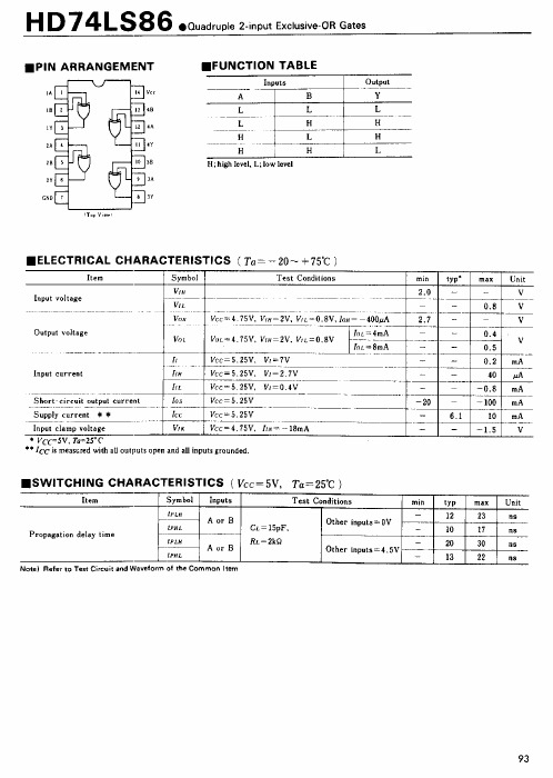
74ls86中文资料_数据手册_参数
Singapore 049318
Harbour City, Canton Road, Tsim Sha Tsui,
Tel: 535-2100
Kowloon, Hong Kong
Fax: 535-1533
Tel: <852> (2) 735 9218
Fax: <852> (2) 730 0281
Hitachi Asia Ltd.
Hitachi Europe GmbH Electronic components Group Dornacher Stra§e 3 D-85622 Feldkirchen, Munich Germany Tel: <49> (89) 9 9180-0 Fax: <49> (89) 9 29 30 00
DP-14 Conforms Conforms 0.97 g
10.06 10.5 Max
14
8
5.5
1
7
1.42 Max
0.10 ± 0.10
1.27
*0.42 ± 0.08 0.40 ± 0.06
0.15 0.12 M
*Dimension including the plating thickness Base material dimension
For further information write to:
tel72系列温控器说朋书

tel72系列温控器说朋书Tel72温湿度控制器,主要应用于需要对被测环境进行自动温湿度调节的场合,用户可通过按键分别调整温湿度的上、下限值来控制加热或排风实现自动控制,显示方式为数码管显示。
温度测量范围:-25℃~+80℃±1℃;湿度测量范围:相对湿度RH:0%~99%精度±3%RH;控制方式:温度采用上、下限和回差控制,湿度采用上、下限控制,所有参数均可设置;输出控制类型:两组继电器触点,分别为加热和排风,每路最大负载AC250V/3A,均为有源输出。
电源:AC220V±20%工作环境:温度:-25℃~+55℃,相对湿度:<95%RH控制设定范围:温度:0℃~80℃,相对湿度:50%RH~99%RH 本机功耗:<3W自检功能:若数码管显示“–––”,则为检测到传感器故障;若加热或排风运行过程中相应指示灯熄灭,则检测到加热或排风故障。
温度控制:当被测环境温度低于设定温度下限时,本仪器启动电加热设备开始加温,此时加热指示灯亮,温度升至比下限温度设定值高回差值时,即:W测≥W下限+回差,停止加温。
当被测环境温度高于设定温度上限时,本仪器启动降温设备(如风机或空调)开始降温,此时排风指示灯亮,温度降至比上限温度设定值低回差值时,即:W测≤W上限-回差,停止降温。
湿度控制:当被测环境湿度超过设定湿度上限时。
如果当前温度较高,即:W测≥W下限+(W上限-W下限)×3÷4,采用降温(或排风,视具体地区采用不同设备)抽湿,此时排风指示灯亮;抽湿过程中,如果温度低于下限温度+2度后,自动转为加热降湿;当降湿过程中温度高于上限温度-2度后,自动转为降温抽湿,直至湿度低于设定下限值为止。
- 1、下载文档前请自行甄别文档内容的完整性,平台不提供额外的编辑、内容补充、找答案等附加服务。
- 2、"仅部分预览"的文档,不可在线预览部分如存在完整性等问题,可反馈申请退款(可完整预览的文档不适用该条件!)。
- 3、如文档侵犯您的权益,请联系客服反馈,我们会尽快为您处理(人工客服工作时间:9:00-18:30)。
Typical Operating Circuit
CT
THRM
2.7V TO 5.5V INPUT
MAX8672
IN
CHGV DR CHGI TRKI
BACKUP BATTERY CONNECTION
FBL BATT
LDO UV
BST GND LX
1.75V 3.05V
________________________________________________________________ Maxim Integrated Products 1
Continuous Power Dissipation (TA = +70°C) 14-Pin, 3mm x 3mm TDFN (derate 18.2 mW/°C above +70°C) .........................1454.5mW
Operating Temperature Range ...........................-40°C to +85°C Junction Temperature ......................................................+150°C Storage Temperature Range .............................-65°C to +150°C Lead Temperature (soldering, 10s) .................................+300°C
ELECTRICAL CHARACTERISTICS
(VIN = 3.6V, TA = -40°C to +85°C, CCT = 0.1µF, unless otherwise noted.) (Note 1)
PARAMETER IN Voltage Range IN Undervoltage Lockout Threshold IN Supply Current
For pricing, delivery, and ordering information, please contact Maxim/Dallas Direct! at 1-888-629-4642, or visit Maxim’s website at .
/
0.1mA ≤ IBATT(CHG) ≤ 1mA, VIN - VBATT > 400mV
TA = -40oC to +85oC
IBATT(TRK) = 1mA IBATT(TRK) = 0.1mA IBATT(TRK) IBATT(CHG)
TA = -40oC to +85oC TA = 0oC to +85oC TA = -40oC to +85oC
TRKI Resistor Range
Charger Dropout Voltage
TA = -40°C to +85°C
VBATT = 1.55V, VBST = 3.3V, VIN = 0V, VBATT(CHG) = 1.5V
VBAVBATT = 3.0V, VIN = 0V
TA = +25oC TA = +85oC
Internal Load Current on BST (Note 2)
BATT Quiescent Supply Current—Backup Mode BATT Quiescent Supply Current—Charging
BATT Leakage Current to IN
Total BATT Battery Leakage Current During UVLO (BATT, LX, and DR Leakage) CHARGER AND BATTERY
Stresses beyond those listed under “Absolute Maximum Ratings” may cause permanent damage to the device. These are stress ratings only, and functional operation of the device at these or any other conditions beyond those indicated in the operational sections of the specifications is not implied. Exposure to absolute maximum rating conditions for extended periods may affect device reliability.
CONDITIONS
VIN rising, hysteresis = 100mV (typ)
VBATT > VBATT(CHG)
VBST = 3.3V, no BST or LDO load, boost and LDO on
VIN = 3.3V VIN = 0V TA = -40°C to +50°C
UVLO
o Reverse Current Blocking on BATT, LDO, and Boost—No Diodes Needed
o No Battery Drain When Off (< 50nA) o Thermistor Sensing Disables Standard Charge o Battery Restart Charge Threshold Prevents
The MAX8672 is available in a 14-pin, 3mm x 3mm TDFN package and is rated for -40°C to +85°C operation.
Applications
PDA, Palmtop, and Wireless Handhelds
MAX8672
19-0653; Rev 0; 11/06 EVAALVUAAILTAIOBNLEKIT
Complete Backup Management IC for NiMH Batteries
General Description
The MAX8672 complete power manager for backup batteries in smart devices offers feature-programmable battery charging and main-system backup. The device includes a charger for 1- or 2-cell NiMH backup batteries. A low-quiescent current synchronous-rectified boost converter and LDO supply up to 20mA during system backup. The BST output is internally set to regulate at 3.05V. The MAX8672 LDO is powered from the boost converter output and is adjustable from 1.5V to 3.05V.
MAX8672
Complete Backup Management IC for NiMH Batteries
ABSOLUTE MAXIMUM RATINGS
IN, BATT, BST, LDO, UV to GND ..........................-0.3V to +6.0V FBL to GND ...............................................-0.3V to (VBST + 0.3V) CT, CHGI, TRKI, CHGV, THRM,
VBATT = 0 to 3.0V
TA = -40°C to +50°C TA = +85oC
CHGI Current-Limit Accuracy
1mA ≤ IBATT(CHG) ≤ 20mA, VIN - VBATT > 400mV
IBATT(CHG) = 1mA, VIN VBATT > 400mV
Smart Cell Phones
Pin Configuration
GND
TOP VIEW
THRM
CHGV
FBL
LDO
14 13 12 11 10 9 8
BST
LX
MAX8672
1234567
TDFN (3mm x 3mm)
UV
DR
IN
BATT
TRKI
CHGI
CT
Features
o Charges 1- or 2-Cell NiMH Backup Batteries o Programmable Charge Current o DC Trickle Charge Mode for Maximum Cell Life o Deep-Recovery Charge Restores Cells < 1V o Programmable Charge Timer o Programmable Charge-Voltage Limit and Battery