爱普生(EPSON)实时时钟模块RA8803SA规格书
GM8803A说明书

1、概述GM8803A型显示控制仪是一种多用途的仪表。
测量速度快,精度高。
它拥有的许多特殊性能很适合称重显示及控制应用。
此外具备清零,零位跟踪,数字滤波,变动检测,峰值、谷值检测及保持功能。
能处理双极性正负信号,与各类荷重传感器、拉压传感器、扭矩传感器配合。
很适合用于试验机控制设备。
●适用于各种电阻应变式测力与称重传感器。
(也适用于扩散硅压力传感器;直流电流、电压信号,需在订货时注明)●16mm高亮度LED显示。
●可选择显示毛重和净重。
●数字滤波、显示分度、显示小数点位置选择功能。
超载时显示。
●自动零位跟踪.●轻触式按键自动去皮。
●采样及测控速度50次/秒●峰值、谷值检测、显示功能。
●接通电源自诊断功能。
●可选择模拟量输出●全透明、高速、高效的网络化通讯接口,实现计算机与仪表间完全的数据传送和控制.独有的控制权转移功能使计算机可以直接控制仪表的报警输出和变送输出。
读取一次测量数据的时间小于10ms提供测试软件,组态软件和应用软件技术支持GM8803A型仪表采用单片机嵌入式组合设计,硬件扩充性强,软件平台灵活,可以扩展开关量输入、定时、程序顺序控制等,不局限于标准功能。
可按实际需要组合,以实现最佳性能.2、型号规格1 2 3 4 5 6 7 8 9GM8803A —☐☐☐☐☐ B☐ S☐☐☐1:面板形式H:横式 S:竖式2:显示方式1:单显示 2:双显示3:输入信号M:直流mV V:直流V I:直流mA4:报警输出方式,无报警可省略TR:继电器输出 TO:OC门输出5:变送输出A:表示带变送输出功能,不带可省略6:外供传感器、变送器电源规格B1:外供24V DC B2:外供12V DC B3:外供精密10V桥压B4:外供精密1mA恒流源 B5:其它7:通讯接口S0:无通讯接口 S1:RS-232接口S2:RS—485接口 S3:RS—422接口S4:BCD码接口8:打印功能P:表示带打印功能,不带可省略9:非标准功能N:表示非标准功能。
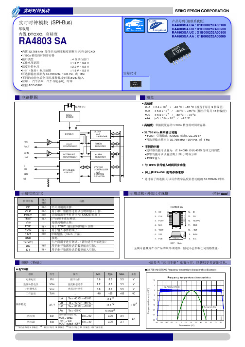
爱普生(EPSON)实时时钟模块RA4803SA规格书
DIVIDER
FOUT CONTROLLER
INTERRUPT CONTROLLER
INTERFACE CIRCUIT
CLOCK and CALENDAR
TIMER REGISTER
ALARM REGISTER
SYSTEM CONTROLLER
and CONTROL REGISTER
• •UA •UB •UC •AA
± 3.4 x 10⁻⁶ / -40 ºC ~ +85 ºC 商
± 5.0 x 10⁻⁶ / -40 ºC ~ +85 ºC 商 ± 5.0 x 10⁻⁶ / -30 ºC ~ +70 ºC (+5 ± 5.0) x 10-6 / +25 ºC
9
器
13
器
•
:
1/100s
●为汽车行驶安全方面的应用(引擎控制单元、气囊、电子稳定程序控制系统)。
注意事项
·本材料如有变更,恕不另行通知。量产设计时请确认最新信息。 ·未经 Seiko Epson 公司书面授权,禁止以任何形式或任何方式复制或者发布本材料中任何部分的信息内容。 ·本材料中的书面信息、应用电路、编程、使用等内容仅供参考。Seiko Epson 公司对第三方专利或版权的侵权行为不负有任何责任。本材料
0
-5
-10
-15 Tuning fork X'tal
-20
-25
-30 -45 -35 -25 -15 -5 5 15 25 35 45 55 65 75 85 Temperature (ºC)
推进环境管理体系 符合国际标准
在环境管理体系的运行方面,使用 ISO14001 国际环境标准,通过“计 划-实施-检查-验证(PDCA)的循环来实现持续改进。公司位于日本和 海外的主要制造基地已取得了 ISO14001 资格认证。
iclock30068088035寸彩屏系列用户手册范本

3.5寸彩屏系列用户手册版本:3.6.2日期:2011年5月内容介绍本文档主要介绍了3.5寸彩屏系列产品的界面及菜单的功能操作。
特别提示本系列指纹机只能与发布的V3.X版考勤软件配套使用。
V3.X 版软件可兼容原V2.X版适用的所有机器,功能比V2.X版有所增强,使用更方便,更加人性化。
请首先阅读操作本机器请先通读本手册。
注意请不要将设备放在强光直照的地方,强光对指纹采集有着明显的影响,会导致指纹验证无法通过。
尽量不要在室外使用,避免强光直射。
指纹机工作的温度范围为0-400C ,长期在室外使用,加上设备本身的发热,容易导致设备工作受到影响,反应可能会变慢,通过率降低。
如果必须在室外使用,建议采用遮阳伞和散热设备。
请不要剧烈碰撞设备,可能会导致设备内部部件松动或损坏。
并且设备不具有防水特性,请勿让本机器淋雨或受潮。
本公司提醒您正确使用,您将得到良好的使用效果和验证速度。
3. 按压指纹的方式安装好指纹机后,再进行指纹登记及比对操作安装 登记 识别登记 安装 识别推荐使用食指、中指或无名指;避免大拇指和小拇指(因为它们按压采集窗口时通常很笨拙)。
按压指纹的方式使用须知1) 正确的手指按压示意图:2) 几种错误的按压方式:●由于产品的不断更新,本公司不能承诺实际产品与该资料一致,同时也不承担由于实际技术参数与本资料不符所导致的任何争议,任何改动恕不提前通知。
● 本手册中 ★ 标示的功能并非所有机器具备。
请以实际产品为准。
●本文档中的图片说明,可能与您手中产品的图片不符,请以实际产品显示为准。
关于本手册手指平压于指纹采集窗口上 指纹纹心尽量对正窗口中心倾斜太靠下垂直 太偏各机型的按键功能不一样,请首先阅读附录中的键盘说明。
关于使用推荐使用步骤:步骤一:安放好机器并给机器通电。
步骤二:用户登记,并登记指纹、密码或卡,分配权限。
步骤三:用户验证,确认登记指纹、密码或卡是可用的。
步骤四:设置好通讯参数,使用与电脑连接的3种方式中的任一方式将员工信息下载至软件。
Seiko Epson RTC-4543SA SB实时时钟模块应用手册说明书

ETM09E-03Real Time Clock ModuleRTC-4543SA/SB•These products are intended for general use in electronic equipment. When using them in specific applications that require extremelyobtain permission from Seiko Epson in advance./ Space equipment (artificial satellites, rockets, etc.) / Transportation vehicles and related(automobiles, aircraft,Submarine transmitters / Power stations and related / Fire work equipment and securityequipment / traffic control equipment / and others requiring equivalent reliability.•All brands or product names mentioned herein are trademarks and/or registered trademarks of their respective.CONTENTS1. OVERVIEW (1)2. BLOCK DIAGRAM (1)3. PIN CONNECTIONS (2)4. PIN FUNCTIONS (2)5. ELECTRICAL CHARACTERISTICS (3)5-1.A BSOLUTE M AXIMUM R ATINGS (3)5-2.O PERATING C ONDITION (3)5-3.F REQUENCY C HARACTERISTICS (3)5-4.DC C HARACTERISTICS (3)5-5.AC C HARACTERISTICS (4)5-6.T IMING C HARTS (5)6. TIMER DATA ORGANIZATION (6)7. DESCRIPTION OF OPERATION (7)7-1.D ATA READS (7)7-2.D ATA WRITES (7)7-3.D ATA WRITES (D IVIDER R ESET) (8)7-4.FOUT OUTPUT AND 1H Z CARRIES (8)8. EXAMPLES OF EXTERNAL CIRCUITS (9)9. EXTERNAL DIMENSIONS (10)10. LAYOUT OF PACKAGE MARKINGS (10)11. REFERENCE DATA (11)12. APPLICATION NOTES (12)32-kHz Output Serial RTC ModuleRTC - 4543 SA/SBBuilt-in crystal permits operation without requiring adjustmentBuilt-in time counters (seconds, minutes, hours) and calendar counters (days, days of the week months, years)Operating voltage range: 2.5 V to 5.5 VSupply voltage detection voltage: 1.7 ±0.3 VLow current consumption: 1.0 µA/2.0 V (Max.)Automatic processing for leap yearsOutput selectable between 32.768 kHz/1 Hz1. OverviewThis module is a real-time clock with a serial interface and a built-in crystal oscillator. This module is also equipped with clock and calendar circuits, an automatic leap year compensation function, and a supply voltage detection function.In addition, this module has a 32.768 kHz/1 Hz selectable output function for hardware control that is independent of the RTC circuit.This module is available in a compact SOP 14-pin package (RTC-4543SA) and a thin SOP 18-pin package (RTC-4543SB).4. Pin FunctionsSignalPin No.SOP-14pin(SOP-18pin)I/O FunctionGND1( 9 )Connects to negative (-) side (ground) of the power supply.CE3( 8 )InputChip enable input pin.When high,the chip is enabled. When low,the DATA pin goes tohigh impedance and the CLK,DATA,and WR pins are not able toaccept input.In addition, when low,the TM bit is cleared.FSEL4( 7 )InputSerect the frequency that is output from the FOUT pin.High : 1 HzLow : 32.768 kHzWR5( 6 )InputDATA pin input/output switching pin.High : DATA input (when writing the RTC)Low : DATA output (when reading the RTC)FOE6( 5 )InputWhen high, the frequency selected by the FSEL pin is output fromthe FOUT pin.When low, the FOUT pin goes to high impedance.V DD9( 14 )Connects to positive (+) side of the power supply.CLK10( 12 )InputSerial clock input pin.Data is gotten at the rising edge during a write, and data is outputat the rising edge during a read.DATA11( 11 )Bi-directional Input/outout pin that is used for writing and reading data.FOUT14( 10 )OutputOutputs the frequency selected by the FSEL pin. 1 Hz output issynchronized with the internal one-second signal.This output is not affected by the CE pin.N.C.2,7,8,12,13( 1,2,3,4,13,15,16,17,18 )Although these pins are not connected internally,they shouldalways be left open in order to obtain the most stable oscillationpossible.* Always connect a passthrough capacitor of at least 0.1 µF as close as possible between V DD and GND.5. Electrical Characteristics5-1. Absolute Maximum RatingsItem Symbol Conditions Min. Max. Unit Supply voltage V DD-0.3 7.0 VInput voltage V I Ta=+25 °C GND-0.3 V DD+0.3 VOutput voltage V O GND-0.3 V DD+0.3 V Storage temperature T STG- -55 +125 °C5-2. Operating ConditionItem Symbol Conditions Min. Max. Unit Operating supplyV DD- 2.5 5.5 V voltageData holding voltage V CLK- 1.4 5.5 VOperating temperature T OPR No condensation-40 +85 °C5-3. Frequency CharacteristicsItem Symbol Conditions Max. Unit Frequency tolerance ∆f/f O Ta=+25 °C , V DD=5.0 V 5 ± 23 * ×10-6Frequency temperatureT op-10to+70 °C +25 °C ref + 10 / - 120 ×10-6 characteristicsFrequency voltagef/V Ta=+25 °C , V DD=2.0 to 5.5 V ± 2 ×10⁻⁶/V characteristicsOscillation start time t STA Ta=+25 °C , V DD=2.5 V 3 s Aging fa Ta=+25 °C , V DD=5 V , first year ± 5 ×10⁻⁶ * Monthly deviation: Approx. 1 min.5-4. DC CharacteristicsUnless specified otherwise: V DD = 5 V ± 10 %, Ta = - 40 to +85 °C Item Symbol Conditions Min. Typ. Max. Unit Current consumption(1) I DD1 V DD=5.0 V CE=L , FOE=L 1.5 3.0 µA Current consumption(2) I DD2 V DD=3.0 V FSEL=H 1.0 2.0 µA Current consumption(3) I DD3 V DD=2.0 V 0.5 1.0 µA Current consumption(4) I DD4 V DD=5.0 V CE=L , FOE=H 4.0 10.0 µA Current consumption(5) I DD5 V DD=3.0 V FSEL=L 2.5 6.5 µA Current consumption(6) I DD6 V DD=2.0 V No load on the1.5 4.0 µAFOUT pinInput voltage V IH WR,DATA,CE,CLK, 0.8 V DD VV IL FOE,FSEL pins 0.2 V DD V0.5 µAInput off/leak current I OFF WR,CE,CLK,FOE,FSEL pinsV IN = V DD or GNDV OH(1)V DD=5.0 V I OH=-1.0 mA 4.5 V Output voltage V OH(2)V DD=3.0 V DATA , FOUT pins 2.0 VV OL(1)V DD=5.0 V I OL= 1.0 mA 0.5 VV OL(2)V DD=3.0 V DATA , FOUT pins0.8 VOutput load conditionN / CL FOUT pin 2 LSTTL / 30 pF Max.( fanout )Output leak current I OZH V OUT=5.5 V DATA , FOUT pins-1.0 1.0 µAI OZL V OUT=0 V DATA , FOUT pins-1.0 1.0 µASupply voltage detectionV DT- 1.4 1.7 2.0 V voltage5-5. AC CharacteristicsUnless specified otherwise: Ta = - 40 to +85 °C, CL = 50 pF Item Symbol V DD=5 V ± 10 % V DD=3 V ± 10 % UnitMin. Max. Min. Max.CLK clock cycle t CLK0.75 7800 1.5 7800 µsCLK low pulse width t CLKL0.375 3900 0.75 3900 µsCLK high pulse width t CLKH0.375 3900 0.75 3900 µs CLK setup time t CLKS25 50 nsCE setup time t CES0.375 3900 0.75 3900 µsCE hold time t CEH0.375 0.75 µsCE enable time t CE0.9 0.9 s Write data setup time t SD0.1 0.2 µsWrite data hold time t HD0.1 0.1 µs WR setup time t WRS100 100 nsWR hold time t WRH100 100 ns DATA output delay time t DATD0.2 0.4 µsDATA output floating time t DZ0.1 0.2 µs Clock input rise time t r150 100 nsClock input fall time t f150 100 ns FOUT rise time (CL=30 pF) t r2100 200 ns FOUT fall time (CL=30 pF) t f2100 200 ns Disable time (CL=30 pF) t XZ100 200 nsEnable time (CL=30 pF) t ZX100 200 nsFOUT duty ratio (CL=30 pF) Duty 40 60 40 60 % Wait time t RCV0.95 1.9 µs5-6. Timing Charts[]Duty t t100%H=×( 4 ) Disable/enable6. Timer Data Organization• The counter data is BCD code.• Writes and reads are both performed on an LSB-first basis.MSBLSBSecond ( 0 to 59 )FDTs40s20s10s8s4s2s1Minutes ( 0 to 59 ) * mi40mi20mi10mi8mi4mi2mi1Hour ( 0 to 23 ) * *h20h10h8h4h2h1Day of the week( 1 to 7 )*w4w2w1Day ( 1 to 31 ) * *d20d10d8d4d2d1Month ( 1 to 12 ) TM **mo10mo8mo4mo2mo1Year ( 0 to 99 )y80y40y20y10y8y4y2y1• Calendar counter. From 1 Jan 2001 to 31 Dec 2099, it is updated by an automatic calendar function.If a year is 4 multiples, it is a leap year, then date is updatedin order to 28 Feb, 29 Feb, Mar 1.Because there is the case that a leap year does not match when using data of year of except the Christian era, please be careful.Data of a day of the week run in cycles with 7 from 1.A recommended example are 1=Sun, 2=Mon,,,6=Fri, 7=Sat.• Clock counter. Only 24 hours system is supported. • ∗bits. These bits are used as memory.• TM bit. This is a test bit for shipping test. Always clear this bit to “0”.• FDT bit: Supply voltage detection bit• This bit is set to “1” when voltage of 1.7 ±0.3 V or less is detected between V DD and GND. • The FDT bit is cleared if all of the digits up to the year digits are read.• Although this bit can be both read and written, clear this bit to "0" in case of the write cycle.if the supply voltage is lower than the detection voltage value, the FDT bit is set to “1”.7. Description of Operation2) At the first rising edge of the CLK signal, the clock and calendar data are loaded into the shiftregister and the LSB of the seconds digits is output from the DATA pin.3) The remaining seconds, minutes, hour, day of the week, day, month, and year data is shifted out,in sequence and in synchronization with the rising edge of the CLK signal, so that the data isoutput from the DATA pin.The output data is valid until the rising edge of the 52nd clock pulse; even if more than 52 clockpulses are input,the output data does not change.4) If data is required in less than 52 clock pulses, that part of the data can be gotten by setting theCE pin low after the necessary number of clock pulses have been output.Example: If only the data from “seconds” to “day of the week” is needed:After 28 clock pulses, set the CE pin low in order to get the data from “seconds” to “day ofthe week.”5) When performing successive data read operations, a wait (tRCV) is necessary after the CE pinis set low.6) Note that if an update operation (a one-second carry) occurs during a data read operation,the data that is read will have an error of -1 second.7) Complete data read operations within tCE (Max.) = 0.9 seconds, as described earlier.1) RTC 4543 shifts to data input state by condition of WR terminal ="H",CE terminal ="H".2) Writing-data synchronize to a rising edge of CLK, and it inputs into an RTC from LSB of sec.3) Inside counter less than second is reset between falling edges of first CLK from a rising edge of next CLK.And update of Clock register is prohibited by the first falling edge of CLK.4) In writing of data to RTC, all 52 clock is necessary.When CE goes to LOW before the 52 bits transmission is completed, there is the possibilitythat * ,FDT and a year digit were destroyed.If a serial communication break occurs, do verify 8 bits of* bit andFDTbit and year data.5) In a rising edge of 52 clock, all data is written to RTC. Data after 53 bits is ignored.6) When CE goes to LOW, RTC re-starts update.Please finish write access within 0.9 second = tCE (Max.).7) Between write access and read access, recovery timing(tRCV) is necessary.Please do not set the time and date which is non-existence.7-3. Data writes (Divider Reset)After the counter is reset, carries to the seconds digit are halted.After the data write operation,the prohibition on carries to the seconds counter is lifted by setting the CE pin low.Complete data write operations within tCE (Max.) = 0.9 seconds, as described earlier.7-4. FOUT output and 1 Hz carriesDuring a data write operation, because a reset is applied to the Devider counter (from the 128 Hzlevel to the 1 Hz level) after the CE pin goes high during the time between the falling edge of the first clock cycle and the rising edge of the second clock cycle, the length of the first 1 Hz cycle after thedata write operation is 1.0 s +0 / −7.8ms +t CES+t CLK. Subsequent cycles are output at1.0-second intervals.The 1-Hz signal that is output on FOUT is the internal 1-Hz signal with a 15.6-ms shift applied.8. Examples of External Circuits11. Reference DataNote : This data shows values obtained from a sample lot.12. Application notes1) Notes on handlingThis module uses a C-MOS IC to realize low power consumption. Carefully note the following cautions when handling.(1) Static electricityWhile this module has built-in circuitry designed to protect it against electrostatic discharge, the chip could still be damaged bya large discharge of static electricity. Containers used for packing and transport should be constructed of conductive materials.In addition, only soldering irons, measurement circuits, and other such devices which do not leak high voltage should be used with this module, which should also be grounded when such devices are being used.(2) NoiseIf a signal with excessive external noise is applied to the power supply or input pins, the device may malfunction or "latch up."In order to ensure stable operation, connect a filter capacitor (preferably ceramic) of greater that 0.1 µF as close as possible to the power supply pins (between VDD and GNDs). Also, avoid placing any device that generates high level of electronic noise near this module.* Do not connect signal lines to the shaded area in the figure shown in Fig. 1 and, if possible, embed this area in a GND land.(3) Voltage levels of input pinsWhen the input pins are at the mid-level, this will cause increased current consumption and a reduced noise margin, and can impair the functioning of the device. Therefore, try as much as possible to apply the voltage level close to VDD or GND.(4) Handling of unused pinsSince the input impedance of the input pins is extremely high, operating the device with these pins in the open circuit state can lead to unstable voltage level and malfunctions due to noise. Therefore, pull-up or pull-down resistors should be provided for all unused input pins.2) Notes on packaging(1) Soldering heat resistance.If the temperature within the package exceeds +260 °C, the characteristics of the crystal oscillator will be degraded and it may be damaged. The reflow conditions within our reflow profile is recommended. Therefore, always check the mounting temperature and time before mounting this device. Also, check again if the mounting conditions are later changed.* See Fig. 2 profile for our evaluation of Soldering heat resistance for reference.(2) Mounting equipmentWhile this module can be used with general-purpose mounting equipment, the internal crystal oscillator may be damaged in some circumstances, depending on the equipment and conditions. Therefore, be sure to check this. In addition, if the mounting conditions are later changed, the same check should be performed again.(3) Ultrasonic cleaningDepending on the usage conditions, there is a possibility that the crystal oscillator will be damaged by resonance during ultrasonic cleaning. Since the conditions under which ultrasonic cleaning is carried out (the type of cleaner, power level, time, state of the inside of the cleaning vessel, etc.) vary widely, this device is not warranted against damage during ultrasonic cleaning.(4) Mounting orientationThis device can be damaged if it is mounted in the wrong orientation. Always confirm the orientation of the device before mounting.(5) Leakage between pinsLeakage between pins may occur if the power is turned on while the device has condensation or dirt on it. Make sure the device is dry and clean before supplying power to it.Application ManualElectronic devices information on WWW serverDistributor/en/quartz/index.html。
ra8803技术通报
RAiO TECHNOLOGY INC.
wwຫໍສະໝຸດ
(请进入本公司网页会员中心下载 ) 适 用 晶 片: 1. Date Code 为 0415 之后的 RA8822/8803 芯片 2. 2004 年 3 月 20 日之后出货的 RA8822/8803 芯片 状 况 说 明: RA8822 及 RA8803 用于某些 240x128 点阵和 160x128 点阵模块时,显示效果不够理想。 1. 请在缓存器的初始设定时,将缓存器[81h]的值有设成40h。 2. 如果缓存器[81h]的值有设成00h(初始值) ,显示画面会不均匀,同时显示一段时间后画面变 淡。 建 3. 不论使用的模块分辨率为何,都建议进行此设定。 议 及 解 决 方 式 :
技术通报
T01_2005
产 品 名 称: 通 报 对 象: 参 考 文 件: RA8803/8822 代理商、模块厂、系统厂 Data Sheet V2.2 之后的版本(含 2.2 版) AP Note V2.3 之后的版本(含 2.3 版) RA8803_8822_DS_v22_GB.pdf RA8803_8822_AP_v23_GB.pdf 日 期: April 22, 2005
RTC实时时钟芯片

RTC实时时钟芯片RTC实时时钟芯片是一种计时器,可以由硬件集成电路来完成,也可以由单片机加程序来完成。
实时时钟可以对秒、分、时、星期、日、月和年进行准确计时,具有闰年补偿功能,能够计时到2100年。
消费类电子(机顶盒、VCR),手持式装置(GPS、POS终端),医疗设备,办公设备,电信(路由器、交换机、服务器),电器设备,汽车,消费类电子,嵌入式时标,工业,电表。
DS3231集成了温度补偿晶体振荡器(TCXO)和晶体,电池备份输入用于支持连续计时,可编程方波输出,低电平有效复位输出。
关键参数:工作温度商业级:0°C至+70°C,具有2ppm精度;工业级:40°C至+85°C,具有3.5pmm精度。
DS3231M是业内首款内置MEMS、带温度补偿的RTC,允许器件用于强烈震动的场合,不会由于晶体失效而导致产品故障。
DS3232相比较于DS3231将32kHz输出驱动器更改为推挽输出,省去一个外部上拉电阻,节省空间,够加快时钟的边沿速度,降低器件功耗。
电池切换时,可通过32kHz位选择使能/禁止32kHz输出。
DS3232的32kHz输出在关闭状态下驱动至低电平,DS3231的32kHz输出在关闭状态下为高阻输出。
DS3232内部可通过2个CRATE位控制温度转换速率,这些位用于控制器件的采样率。
采样率决定了对温度传感器进行数字转换的频率,以及补偿振荡器的时间间隔。
降低采样率则降低了温度传感器的工作频率,从而降低整体功耗。
此外,DS3232具有236字节的SRAM。
压检测功能和振荡停止检测功能,内置定时器可以产生周期性的定时中断信号,警报器用于定时报警,可设定天、日期、小时、分钟。
工作电压范围:1.70V-5.5V。
计时保持电压:1.15V-5.5V。
此外,采用IIC接口,支持低功耗模式。
RX6110频率输出功能:能选择输出频率,有32.768kHz, 1024Hz, 1Hz。
RA8803(8822)
RAiO TECHNOLOGY INC.
2/57
Version 2.6
章节
RA8803/8822
双图层中文文字/图形 LCD 控制器
内
容
页数
1. 简介................................................................................................... 5 2. 特性................................................................................................... 5 3. 系统方块图.......................................................................................... 6 4. 脚位定义............................................................................................. 8
5.缓存器描述..........................................................................................13
5-1 缓存器总表 ............................................................................................................................................... 13 5-2 缓存器内容描述 ........................................................................................................................................ 14 5-3 窗口大小设定缓存器................................................................................................................................. 29
爱普生PDG53P0800P5DN电流保护模具说明书

Eaton PDG53P0800P5DNEaton Power Defense molded case circuit breaker, Globally Rated, Frame 5, Three Pole, 800A, 100kA/480V, PXR25 ARMS LSIG w/ Modbus RTU, CAM Link and Relays, No TerminalsEaton Power Defense molded case circuit breakerPDG53P0800P5DN 786679291481139.7 mm 406.4 mm 209.5 mm 21.32 kg Eaton Selling Policy 25-000, one (1) year from the date of installation of theProduct or eighteen (18) months from thedate of shipment of the Product,whichever occurs first.RoHS Compliant IEC 60947-2CCC MarkedUL 489CSAProduct NameCatalog Number UPCProduct Length/Depth Product Height Product Width Product Weight WarrantyCompliancesCertificationsModbus / Relays / CAM100 kAIC at 480 Vac5600800 AThree-pole600 VPD5 Global100 kAIC Icu/ 50 kAIC Ics/ 220 kAIC Icm @380-415V (IEC)85 kAIC Icu/ 40 kAIC Ics/ 187 kAIC Icm @480V Brazil (IEC)200 kAIC @240V (UL)100 kAIC Icu/ 50 kAIC Ics/ 220 kAIC Icm @440V (IEC)100 kAIC @480/277V (UL)35 kAIC Icu/ 18 kAIC Ics/ 73.5 kAIC Icm @690V (IEC)200 kAIC Icu/ 150 kAIC Ics/ 440 kAIC Icm @240V (IEC)40 kAIC Icu/ 25 kAIC Ics/ 84 kAIC Icm @525V South Africa (IEC) 65 kAIC @600/347V (UL)ElectronicClass AComplete breakerNo Terminals600 Vac Eaton Power Defense MCCB PDG53P0800P5DN 3D drawingConsulting application guide - molded case circuit breakersPower Xpert Protection Manager x64Power Xpert Protection Manager x32StrandAble terminals product aidPower Defense brochurePower Defense molded case circuit breaker selection posterPower Defense technical selling bookletPower Defense molded case circuit breakers - Frame 5 product aid Power Xpert Release trip units for Power Defense molded case circuit breakersMolded case circuit breakers catalogPDG5 CSA CertificationPDG5 CB reportEU Declaration of Conformity - Power Defense molded case circuit breakersPDG5 UL authorizationPower Defense Declaration concerning California’s Proposition 65PDG6 CCC certificatePDG6 CSA certificationPDG5 CCC certificationPower Defense Frame 5 walking beam installation instructions -IL012290ENPower Defense Frame 5 key interlock installation instructions -IL012294ENPower Defense Frame 5 breaker status module installation instructions – IL012307ENPower Defense Frame 4_5 flex shaft handle mech assembly instructions - IL012284ENPower Defense Frame 5 interphase barrier kit 3 pole installation instructions - IL012293ENPower Defense Frame 4_5_6 high performance flex shaft handle mechSpecial featuresInterrupt ratingFrameRated operation voltage (Ue) at AC - max Amperage RatingNumber of polesVoltage rating - maxCircuit breaker typeInterrupt rating rangeSwitch off techniqueClassCircuit breaker frame typeTerminalsVoltage rating 3D CAD drawing package Application notesBrochuresCatalogsCertification reports Installation instructionsPXR 25 LSIG w/ARMS Modbus RTU and CAM Link assembly instructions - IL012296ENPower Defense Frame 5 vertical padlockable handle lock hasp installation instructions - IL012283ENPower Defense Frame 2/3/4/5/6 voltage neutral sensor module wiring instructions – IL012316ENPower Defense Frame 5 aux, alarm, shunt trip and uvr instructions(IL012201EN).pdfPower Defense Frame 5 Trip Unit Upgrade Relays Board, Animated Instructions.rhPower Defense Frame 5 Trip Unit Replacement Animated Instructions Power Defense Frame 5 Shunt Trip, Aux and Alarm Trip How-To Video Power Defense Frame 5 Aux, Alarm, ST and UVR Animated Instructions.rh1Power Defense Frame 5 UVR Trip How-To VideoPower Defense Frame 5 Trip Unit Upgrade Wire Harnesses, Animated Instructions.rhPower Defense Frame 6 Trip Unit How-To VideoPower Defense BreakersPower Defense Frame 2 Variable Depth Rotary Handle Mechanism Installation How-To VideoPower Defense molded case circuit breakersPower Defense Frame 5 Trip Unit How-To VideoPower Defense Frame 3 Variable Depth Rotary Handle Mechanism Installation How-To VideoEaton Power Defense for superior arc flash safetyEaton Specification Sheet - PDG53P0800P5DNPower Defense time current curve Frame 5 - PD5Selling Policy 25-000 - Distribution and Control Products and ServicesImplementation of arc flash mitigating solutions at industrial manufacturing facilitiesSingle and double break MCCB performance revisitedMolded case and low-voltage power circuit breaker healthMaking a better machineIntelligent circuit protection yields space savingsTrip TypeCommunicationInstallation videosMultimediaSpecifications and datasheetsTime/current curvesWarranty guidesWhite papersEaton Corporation plc Eaton House30 Pembroke Road Dublin 4, Ireland © 2023 Eaton. All Rights Reserved. Eaton is a registered trademark.All other trademarks areproperty of their respectiveowners./socialmediaIntelligent power starts with accurate, actionable data Safer by design: arc energy reduction techniques Molded case and low-voltage breaker health。
- 1、下载文档前请自行甄别文档内容的完整性,平台不提供额外的编辑、内容补充、找答案等附加服务。
- 2、"仅部分预览"的文档,不可在线预览部分如存在完整性等问题,可反馈申请退款(可完整预览的文档不适用该条件!)。
- 3、如文档侵犯您的权益,请联系客服反馈,我们会尽快为您处理(人工客服工作时间:9:00-18:30)。
DTCXO,
RA8803 SA
• 32.768 kHz
(
) DTCXO
•1/100s •
: I2C-Bus (400kHz)
•
: 1.6 V ~ 5.5 V
•
: 2.2 V ~ 5.5 V
•
: 1.6 V ~ 5.5 V
•
32.768 kHz, 1024 Hz, 1Hz.
•
,
,
,EVIN
FOE FOUT EVIN / INT
SDA SCL
32.768 kHz
32kHz DTCXO
DIVIDER
FOUT CONTROLLER
INTERRUPT CONTROLLER
INTERFACE CIRCUIT
CLOCK and
CALENDAR
TIMER REGISTER
ALARM REGISTER
5 32.768 kHz DTCXO
0
-5
-10
-15 Tuning fork X'tal
-20
-25
-30 -45 -35 -25 -15 -5 5 15 25 35 45 55 65 75 85 Temperature (ºC)
推进环境管理体系 符合国际标准
在环境管理体系的运行方面,使用 ISO14001 国际环境标准,通过“计 划-实施-检查-验证(PDCA)的循环来实现持续改进。公司位于日本和 海外的主要制造基地已取得了 ISO14001 资格认证。
CONTROL REGISTER and
SYSTEM CONTROLLER
T1(CE)
SCL
FOUT
TEST
VDD
-
FOE
EVIN
/ INT
GND
-
T2(VPP)
-
SDA
( CMOS
)
FOUT
( N-ch
)
属
• •UA •UB •UC •AA
± 3.4 x 10⁻⁶ / -40 ºC ~ +85 ºC 商
未对任何专利或知识版权的许可权进行授权。 ·本材料中规格表中的数值大小通过数值线上的大小关系表示。 ·当出口此材料中描述的产品或技术时,你应该遵守相应的出口管制法律和法规,并按照这些法律和法规的要求执行。
请不要将产品(以及任何情况下提供任何的技术信息)用于开发或制造大规模杀伤性武器或其他军事用途。还要求,不要将产品提供给任何 将产品用于此类违禁用途的第三方。 ·此类产品是基于在一般电子机械内使用而设计开发的,如将产品应用于需要极高可靠性的特定用途,必须实现得到弊公司的事前许可。若 无许可弊公司将不负任何责任。
±5.0 ∗2
× 10-6
AA Ta = +25 ºC
5 ±5.0 ∗3
(1)
IDD1
, VDD = 5V
-
0.75
3.4
(2)
FOE = GND,
IDD2
/INT = VDD FOUT output : OFF
VDD = 3V
-
0.75
2.1
µA
∗1 )
9
∗2 )
13
∗3 )
13
(
)
Frequency tolerance ( ×10-6 )
3.2 ± 0.1
10.1 ± 0.2
14. N.C. 13. SDA 12. T2(VPP) 11. GND 10. / INT
9. EVIN 8. N.C.
∗
32.768 kHz-DTCXO Frequency temperature characteristics (Example)
Min.
Typ.
•
多
多
• AEC-Q200 * I2C-Bus NXP Semiconductor
商
器
RA8803SA UA : X1B0002B000262A00200
RA8803SA UC : X1B000262A00300
RA8803SA AA : X1B000262A00600
Max.
Frequency temperature characteristics
VDD
1.6
3.0
5.5
V
10
VTEM
2.2
3.0
5.5
V
VCLK
1.6
3.0
5.5
V
TOPR
−
-40
+25
+85
ºC
UA Ta = -40 ºC ~ +85 ºC
±3.4 ∗1
∆ f / f UB UC
Ta = -40 ºC ~ +85 ºC Ta = -30 ºC ~ +70 ºC
1.太空设备(人造卫星、火箭等) 2.运输车辆机器控制装置(汽车、飞机、火车、船舶等) 3.用于维持生命的医疗器械 4.海底中转设备 5.发电站控制机器 6.防灾防盗装置 7.交通设备 8.其他,用于与 1~7 具有同等可靠性的用途。
本材料中记载的品牌名称或产品名称是其所有人的商标或注册商标。
Seiko Epson Corporation
• • • • EVIN
1/4096 ,,
4095 .
• 1PPS
•
RX-8801
*
,
32.768kHz .
/
( :mm)
1. T1(CE) 2. SCL 3. FOUT 4. N.C. 5. TEST 6. VDD 7. FOE
1.27
RA8803 SA
5.0 7.4 ± 0.2 SOP − 14 pin
± 5.0 x 10⁻⁶ / -40 ºC ~ +85 ºC 商 ± 5.0 x 10⁻⁶ / -30 ºC ~ +70 ºC (+5 ± 5.0) x 10-6 / +25 ºC
9
器
13
器
•
:
1/100s
• 32.768 kHz • FOUT •
(CMOS ), CL=30 pF 32.768 kHz, 1024 Hz, 1 Hz.
ISO 14000 是国际标准化组织于 1996 年在全球化变暖、臭 氧层破坏、以及全球毁林等环境问题日益严重的背景下提
出的环境管理国际标准。
追求高品质
Seiko Epson 为了向顾客提供高品质、卓越信赖性的产品、服务,迅 速着手通过 ISO 9000 系列资格认证的工作,其日本和海外工厂也在通 过 ISO 9001 认证。同时,也在通过大型汽车制造厂商要求规格的 ISO/TS 16949 认证。
●为汽车行驶安全方面的应用(引擎控制单元、气囊、电子稳定程序控制系统)。
注意事项
·本材料如有变更,恕不另行通知。量产设计时请确认最新信息。 ·未经 Seiko Epson 公司书面授权,禁止以任何形式或任何方式复制或者发布本材料中任何部分的信息内容。 ·本材料中的书面信息、应用电路、编程、使用等内容仅供参考。Seiko Epson 公司对第三方专利或版权的侵权行为不负有任何责任。本材料
ISO/TS16949 是一项国际标准,是在 ISO9001 的基础上增 加了对汽车工业的特殊要求部分。
关于在目录内使用的记号
●无铅。
●符合欧盟 RoHS 指令。 欧盟 RoHS 指令免检的含铅产品。 (密封玻璃、高温熔化性焊料或其他材料中包含铅。)
●为汽车方面的应用,如汽车多媒体、车身电子、遥控无钥门锁等。