Analog In-circuit Testing
analog测试介绍
Analog Source file: "analog/r1" disconnect all
connect s to "c1-1" Relay control connect i to "c1-2" resistor 1.00k, 5, 5, re3, ar100m test ! "r1" test !... High, Low limit
IIG
Module 14-24
impedance in the Guard bus
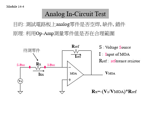
解法:把MOA接在ZIG兩端, 使流經ZIG電流=0
Rref
S-Bus
Rx IRx
I-Bus
Iref
MOA
VMOA
Vs
ZSG
ZIG ZL
G-Bus
L-bus or
Zg
disconnect all connect s to "Rx-1" connect i to "Rx-2" connect g to "Z-1"; l to "Z-1" connect gl to "Z-1" resistor <value, tol, options>
現象: 當ISG流過Zg, 會產生壓降, 壓降越大, 引起ZIG電流越 大
Rref
S-Bus
Rx
IRx
I-Bus
Iref
MOA
VMOA
Vs
ZSG ISG
Zg
G-Bus
ZIG
disconnect all connect s to "Rx-1" connect i to "Rx-2" connect g to "Z-1" resistor <value, tol, options>
Keysight Medalist i1000D In-Circuit Test System 数据

Keysight TechnologiesMedalist i1000D In-Circuit Test SystemData SheetThe Keysight Medalist i1000D In-Circuit Tester (ICT) redefines digital testing by bringing electronics manufacturers easy to use and affordable testing for digital devices.The Keysight Technologies, Inc. Medalist i1000D is now even better. Improving from its previous state of an analog-only ICT, the new digital release of the system now features per pin programmable digital cards and a whole new set of intuitive software graphical user interfaces (GUIs) that makes programming and development effortless.With its new digital capabilities, the Medalist i1000D now can perform digital PCF/VCL library based testing, Boundary Scan and I2C/ SPI serial programming on a simple, low-cost long-wired test fixture. This presents an excellent opportunity for customers who are looking for better test coverage without any increase in cost.The digital subsystem of the i1000D harnesses the simplicity and power from the industry-leading Medalist i3070 ICT, to bring customers the power to adjust test speeds, drive and receive voltages with just a few clicks of the mouseEase of useRetaining all the simple yet intuitive features of the earlier U9401/2A model, thenew Medalist i1000D software adds on to its arsenal with new features that make development and debugging of digital tests as easy as ABC.Following the development model of a typical Manufacturing Defects Analyzer, the user can now get a fixture and program up and running in just a few days. When digital test is required, simply assign the test libraries and power supplies using the new Developer GUI and let the i1000D software do the rest.Simplified GUIs allow the user to quickly make changes to individual tests during debug, with a comprehensive set of menus and buttons, complete with AutoDebug features. This allows inexperienced users to start using the system quickly.With the Medalist i1000D, unpowered passive analog components can be debugged with the click of a button, so even someone with limited ICT experience can perform a complete analog test debug in a matter of hours.AutoDebug fine tunes tests so boards pass reliably in production. Statistical measures (CPK) are employed to determine the stability of the test. This automatic feature can reduce the normal debug process which takes days, to just a few hours.Figure 1. Easy to use Test Developer GUI enables even inexperienced users to deploy a fixture and program in just a few days.Digital test are usually viewed as complex, difficult to understand and debug by many users. With the i1000D, things are different. The digital debug GUI leverages the control and flexibility of the legendary i3070 PushButton debug GUI, allowing engineers and technicians to have full control of the digital test parameters and test source codes, yet making it easy to understand. This is achieved by transforming lines of the complicated digital test source codes into simple, easy to understand graphical waveforms. Engineers and technicians performing debug are shielded from the massive lines of codes.Figure 2. Digital Debugging is made easy on the Medalist i1000D with graphical interface.VTEP v2.0 Powered Test SuiteAwarded to iVTEP Manufacturers facing tough time to market pressures can have peace of mind that with the i1000D,they have access to the best vectorless test solutions in the world to help them quickly find defectson digital devices.The i1000D come with Keysight’s award-winning Medalist VTEP v2.0 Powered vectorless test suite.This suite comprises Network Parameter Measurement, iVTEP and the original Medalist VTEPtechnology. This powerful suite surpasses the traditional Keysight Testjet capabilities and has beenproven to provide better test coverage than tradition digital library tests.And the innovations do not just stop here.Cover-Extend technologyAwarded to Cover-Extend Technology The Medalist i1000D is Cover-Extend ready. In Cover-Extend1 technology, test coverage is no longerlimited by test accessibility or library availability. With Cover-Extend, VTEP test can be performedon devices without needing physical test access, thus lowering fixture costs and reducing thenumber of required test points on the printed circuit board assembly.Network Parameter MeasurementAwarded to Network Parameter Measurement Another industry first, Network Parameter Measurement technology detects defects on powerand ground pins while iVTEP focuses on ultra low value measurement of signal pins (< 5fF) onIntegrated Circuits (ICs). Furthermore, having the original Medalist VTEP as its core means enablingmeasurements which are 4X more sensitive and 5X better in standard deviation. As technologyadvances with shrinking packages and faster signaling speeds, VTEP v2.0 is a necessity to meet thechallenges of today and beyond.Automatic guardThe automatic guard feature is a tool for the production test engineer as well as test programmer. Itautomatically selects different guard points based on board topology for the user during the debugprocess. This eliminates the need for the user to manually check the schematics for each possibleguard point, hence significantly reducing the overall debug time.Complete Boundary Scan Test CapabilitiesPutting even more ICT power in the hands of its users, Keysight has equipped the i1000D with fullboundary scan capabilities, from Standard Boundary Scan and Connect test to Interconnect test.These capabilities help satisfy manufacturers’ test needs for Boundary Scan enabled devices, andwill ensure manufacturers are geared for the future where there will be increased needs to testIntel®-based peripheral control hubs and processors.FixturingLong-wired MDA Press Down fixtures are not suitable for digital tests. Is this true or false?While it is commonly perceived to be true, the Medalist i1000D proves this wrong.The Medalist i1000D runs digital tests using a traditional MDA-style long-wired press down fixture. Boundary Scan tests, Serial Programming, Library-based tests all run without a glitch. Users now have a test solution that is simple and effective, and at the same time keep their operational costs down with the MDA-style fixtures.Figure 3. No cross talk on adjacent channels.1 Vp-p signal measuredat end of flat cableFigure 4. Low signal loss.Programmable receiver0 to 4.85 V Programmable driver0 to 5 VMax sink current Peak 500 mA Max source current Peak 500 mA Pattern rate Max 2 MPS Programmable vector cycle Programmable Programmable vector cycle resolution50 ns Programmable receive delay Programmable Programmable receive delay resolution10 nsPin card Un-multiplexed analog 128 channelsUn-multiplexed hybrid 64 channels Printer Dot-Matrix TM-U220 SeriesThis information is subject to change without notice.© Keysight Technologies, 2010 - 2017Published in USA, September 21, 20175989-6412ENFor more information on KeysightTechnologies’ products, applications or services, please contact your local Keysight office. The complete list is available at:/find/contactus Americas Canada (877) 894 4414Brazil 55 11 3351 7010Mexico001 800 254 2440United States (800) 829 4444Asia Pacific Australia 1 800 629 485China800 810 0189Hong Kong 800 938 693India 1 800 11 2626Japan 0120 (421) 345Korea 080 769 0800Malaysia 1 800 888 848Singapore 180****8100Taiwan0800 047 866Other AP Countries (65) 6375 8100Europe & Middle East Austria 0800 001122Belgium 0800 58580Finland 0800 523252France 0805 980333Germany ***********Ireland 1800 832700Israel 1 809 343051Italy800 599100Luxembourg +32 800 58580Netherlands 0800 0233200Russia 8800 5009286Spain 800 000154Sweden 0200 882255Switzerland0800 805353Opt. 1 (DE)Opt. 2 (FR)Opt. 3 (IT)United Kingdom0800 0260637For other unlisted countries:/find/contactus(BP-9-7-17)/go/quality Keysight Technologies, Inc.DEKRA Certified ISO 9001:2015Quality Management System/find/i1000DEvolving Since 1939Our unique combination of hardware, software, services, and people can help you reach your next breakthrough. We are unlocking the future of technology. From Hewlett-Packard to Agilent to Keysight.myKeysight/find/mykeysightA personalized view into the information most relevant to you. /find/emt_product_registrationRegister your products to get up-to-date product information andfind warranty information.Keysight Services/find/serviceKeysight Services can help from acquisition to renewal across your instrument’s lifecycle. Our comprehensive service offerings—one-stop calibration, repair, asset management, technology refresh, consulting, training and more—helps you improve product quality and lower costs.Keysight Assurance Plans/find/AssurancePlansUp to ten years of protection and no budgetary surprises to ensure your instruments are operating to specification, so you can rely on accurate measurements.Keysight Channel Partners/find/channelpartnersGet the best of both worlds: Keysight’s measurement expertise and product breadth, combined with channel partner convenience.。
ICT Debug Guider

ICT 不良板维修指导前言本资料是用于对测试部ICT debug技术员进行培训所用,主要用于介绍ICT 的一些基本测试流程,常见不良板维修思路,并附有一定数量的维修实例进行详细解剖,分析。
参与培训的技术员要求有一定的电路基础,计算机能力,电子类专业较为适合,对ICT 和夹具有一定的了解。
撰写此材料的目的是为了培养技术员的逻辑思维,判断能力和理解能力,意在缩短新员工的培训时间,使其能够快速入门,成为一名基本合格的技术员。
同时此书也适合一些有一定维修基础的技术员,能够更好的拓展维修思路,提高维修效率。
书中同时也涉及部分夹具方面知识,所有实例均取之项目维修过程中的一些历史维修事件,附有图片,报告,未经允许不得将此书中的任何实例转载。
注意:以下维修方法及经验将默认为测试平台、测试夹具及其测试程序无不良。
(PCBA Level)电气测试使用的最基本仪器是在线测试仪(ICT)。
ICT:测试仪测量时使用专门的针床与已焊接好的线路板上的元器件接触,并用数百毫伏电压和10毫安以内电流进行分立隔离测试,从而精确地测出所装电阻、电感、电容、二极管、三极管、可控硅、场效应管、集成块等通用和特殊元器件的漏装、错装、参数值偏差、焊点连焊、线路板开短路等故障,并将故障是哪个元件或开短路位于哪个点准确告诉用户。
GE ICT测试使用的是HP3070测试平台。
测试流程:Pin TestPre-shortsShortsAnalog In-CircuitTestjetPower SupplyBoundary ScanDigital TestAnalog Functional TestProgramming Devices (Flash, CPLD, EPROM)一.Pin Test这个测试命令是测试所有没有电容隔离的针脚。
这个测试将确保测试设备针脚和待测的板子之间的良好接触。
错误报告中的信息一般包括了发生故障的节点(回路)和在节点上的元件或针脚,如果有很多信息,那么测试机器将给出一个故障的列表。
半导体制造技术
Semiconductor Manufacturing Technology半导体制造技术Instructor’s ManualMichael QuirkJulian SerdaCopyright Prentice HallTable of Contents目录OverviewI. Chapter1. Semiconductor industry overview2. Semiconductor materials3. Device technologies—IC families4. Silicon and wafer preparation5. Chemicals in the industry6. Contamination control7. Process metrology8. Process gas controls9. IC fabrication overview10. Oxidation11. Deposition12. Metallization13. Photoresist14. Exposure15. Develop16. Etch17. Ion implant18. Polish19. Test20. Assembly and packagingII. Answers to End-of-Chapter Review QuestionsIII. Test Bank (supplied on diskette)IV. Chapter illustrations, tables, bulleted lists and major topics (supplied on CD-ROM)Notes to Instructors:1)The chapter overview provides a concise summary of the main topics in each chapter.2)The correct answer for each test bank question is highlighted in bold. Test bankquestions are based on the end-of-chapter questions. If a student studies the end-of-chapter questions (which are linked to the italicized words in each chapter), then they will be successful on the test bank questions.2Chapter 1Introduction to the Semiconductor Industry Die:管芯 defective:有缺陷的Development of an Industry•The roots of the electronic industry are based on the vacuum tube and early use of silicon for signal transmission prior to World War II. The first electronic computer, the ENIAC, wasdeveloped at the University of Pennsylvania during World War II.•William Shockley, John Bardeen and Walter Brattain invented the solid-state transistor at Bell Telephone Laboratories on December 16, 1947. The semiconductor industry grew rapidly in the 1950s to commercialize the new transistor technology, with many early pioneers working inSilicon Valley in Northern California.Circuit Integration•The first integrated circuit, or IC, was independently co-invented by Jack Kilby at Texas Instruments and Robert Noyce at Fairchild Semiconductor in 1959. An IC integrates multiple electronic components on one substrate of silicon.•Circuit integration eras are: small scale integration (SSI) with 2 - 50 components, medium scale integration (MSI) with 50 – 5k components, large scale integration (LSI) with 5k to 100kcomponents, very large scale integration (VLSI) with 100k to 1M components, and ultra large scale integration (ULSI) with > 1M components.1IC Fabrication•Chips (or die) are fabricated on a thin slice of silicon, known as a wafer (or substrate). Wafers are fabricated in a facility known as a wafer fab, or simply fab.•The five stages of IC fabrication are:Wafer preparation: silicon is purified and prepared into wafers.Wafer fabrication: microchips are fabricated in a wafer fab by either a merchant chip supplier, captive chip producer, fabless company or foundry.Wafer test: Each individual die is probed and electrically tested to sort for good or bad chips.Assembly and packaging: Each individual die is assembled into its electronic package.Final test: Each packaged IC undergoes final electrical test.•Key semiconductor trends are:Increase in chip performance through reduced critical dimensions (CD), more components per chip (Moore’s law, which predicts the doubling of components every 18-24 months) andreduced power consumption.Increase in chip reliability during usage.Reduction in chip price, with an estimated price reduction of 100 million times for the 50 years prior to 1996.The Electronic Era•The 1950s saw the development of many different types of transistor technology, and lead to the development of the silicon age.•The 1960s were an era of process development to begin the integration of ICs, with many new chip-manufacturing companies.•The 1970s were the era of medium-scale integration and saw increased competition in the industry, the development of the microprocessor and the development of equipment technology. •The 1980s introduced automation into the wafer fab and improvements in manufacturing efficiency and product quality.•The 1990s were the ULSI integration era with the volume production of a wide range of ICs with sub-micron geometries.Career paths•There are a wide range of career paths in semiconductor manufacturing, including technician, engineer and management.2Chapter 2 Characteristics of Semiconductor MaterialsAtomic Structure•The atomic model has three types of particles: neutral neutrons(不带电的中子), positively charged protons(带正电的质子)in the nucleus and negatively charged electrons(带负电的核外电子) that orbit the nucleus. Outermost electrons are in the valence shell, and influence the chemical and physical properties of the atom. Ions form when an atom gains or loses one or more electrons.The Periodic Table•The periodic table lists all known elements. The group number of the periodic table represents the number of valence shell electrons of the element. We are primarily concerned with group numbers IA through VIIIA.•Ionic bonds are formed when valence shell electrons are transferred from the atoms of one element to another. Unstable atoms (e.g., group VIIIA atoms because they lack one electron) easily form ionic bonds.•Covalent bonds have atoms of different elements that share valence shell electrons.3Classifying Materials•There are three difference classes of materials:ConductorsInsulatorsSemiconductors•Conductor materials have low resistance to current flow, such as copper. Insulators have high resistance to current flow. Capacitance is the storage of electrical charge on two conductive plates separated by a dielectric material. The quality of the insulation material between the plates is the dielectric constant. Semiconductor materials can function as either a conductor or insulator.Silicon•Silicon is an elemental semiconductor material because of four valence shell electrons. It occurs in nature as silica and is refined and purified to make wafers.•Pure silicon is intrinsic silicon. The silicon atoms bond together in covalent bonds, which defines many of silicon’s properties. Silicon atoms bond together in set, repeatable patterns, referred to asa crystal.•Germanium was the first semiconductor material used to make chips, but it was soon replaced by silicon. The reasons for this change are:Abundance of siliconHigher melting temperature for wider processing rangeWide temperature range during semiconductor usageNatural growth of silicon dioxide•Silicon dioxide (SiO2) is a high quality, stable electrical insulator material that also serves as a good chemical barrier to protect silicon from external contaminants. The ability to grow stable, thin SiO2 is fundamental to the fabrication of Metal-Oxide-Semiconductor (MOS) devices. •Doping increases silicon conductivity by adding small amounts of other elements. Common dopant elements are from trivalent, p-type Group IIIA (boron) and pentavalent, n-type Group VA (phosphorus, arsenic and antimony).•It is the junction between the n-type and p-type doped regions (referred to as a pn junction) that permit silicon to function as a semiconductor.4Alternative Semiconductor Materials•The alternative semiconductor materials are primarily the compound semiconductors. They are formed from Group IIIA and Group VA (referred to as III-V compounds). An example is gallium arsenide (GaAs).•Some alternative semiconductors come from Group IIA and VIA, referred to as II-VI compounds. •GaAs is the most common III-V compound semiconductor material. GaAs ICs have greater electron mobility, and therefore are faster than ICs made with silicon. GaAs ICs also have higher radiation hardness than silicon, which is better for space and military applications. The primary disadvantage of GaAs is the lack of a natural oxide.5Chapter 3Device TechnologiesCircuit Types•There are two basic types of circuits: analog and digital. Analog circuits have electrical data that varies continuously over a range of voltage, current and power values. Digital circuits have operating signals that vary about two distinct voltage levels – a high and a low.Passive Component Structures•Passive components such as resistors and capacitors conduct electrical current regardless of how the component is connected. IC resistors are a passive component. They can have unwanted resistance known as parasitic resistance. IC capacitor structures can also have unintentional capacitanceActive Component Structures•Active components, such as diodes and transistors can be used to control the direction of current flow. PN junction diodes are formed when there is a region of n-type semiconductor adjacent to a region of p-type semiconductor. A difference in charge at the pn junction creates a depletion region that results in a barrier voltage that must be overcome before a diode can be operated. A bias voltage can be configured to have a reverse bias, with little or no conduction through the diode, or with a forward bias, which permits current flow.•The bipolar junction transistor (BJT) has three electrodes and two pn junctions. A BJT is configured as an npn or pnp transistor and biased for conduction mode. It is a current-amplifying device.6• A schottky diode is formed when metal is brought in contact with a lightly doped n-type semiconductor material. This diode is used in faster and more power efficient BJT circuits.•The field-effect transistor (FET), a voltage-amplifying device, is more compact and power efficient than BJT devices. A thin gate oxide located between the other two electrodes of the transistor insulates the gate on the MOSFET. There are two categories of MOSFETs, nMOS (n-channel) and pMOS (p-channel), each which is defined by its majority current carriers. There is a biasing scheme for operating each type of MOSFET in conduction mode.•For many years, nMOS transistors have been the choice of most IC manufacturers. CMOS, with both nMOS and pMOS transistors in the same IC, has been the most popular device technology since the early 1980s.•BiCMOS technology makes use of the best features of both CMOS and bipolar technology in the same IC device.•Another way to categorize FETs is in terms of enhancement mode and depletion mode. The major different is in the way the channels are doped: enhancement-mode channels are doped opposite in polarity to the source and drain regions, whereas depletion mode channels are doped the same as their respective source and drain regions.Latchup in CMOS Devices•Parasitic transistors can create a latchup condition(???????) in CMOS ICs that causes transistors to unintentionally(无心的) turn on. To control latchup, an epitaxial layer is grown on the wafer surface and an isolation barrier(隔离阻障)is placed between the transistors. An isolation layer can also be buried deep below the transistors.Integrated Circuit Productsz There are a wide range of semiconductor ICs found in electrical and electronic products. This includes the linear IC family, which operates primarily with anal3og circuit applications, and the digital IC family, which includes devices that operate with binary bits of data signals.7Chapter 4Silicon and Wafer Preparation8z Semiconductor-Grade Silicon•The highly refined silicon used for wafer fabrication is termed semiconductor-grade silicon (SGS), and sometimes referred to as electronic-grade silicon. The ultra-high purity of semiconductor-grade silicon is obtained from a multi-step process referred to as the Siemens process.Crystal Structure• A crystal is a solid material with an ordered, 3-dimensional pattern over a long range. This is different from an amorphous material that lacks a repetitive structure.•The unit cell is the most fundamental entity for the long-range order found in crystals. The silicon unit cell is a face-centered cubic diamond structure. Unit cells can be organized in a non-regular arrangement, known as a polycrystal. A monocrystal are neatly arranged unit cells.Crystal Orientation•The orientation of unit cells in a crystal is described by a set of numbers known as Miller indices.The most common crystal planes on a wafer are (100), (110), and (111). Wafers with a (100) crystal plane orientation are most common for MOS devices, whereas (111) is most common for bipolar devices.Monocrystal Silicon Growth•Silicon monocrystal ingots are grown with the Czochralski (CZ) method to achieve the correct crystal orientation and doping. A CZ crystal puller is used to grow the silicon ingots. Chunks of silicon are heated in a crucible in the furnace of the puller, while a perfect silicon crystal seed is used to start the new crystal structure.• A pull process serves to precisely replicate the seed structure. The main parameters during the ingot growth are pull rate and crystal rotation. More homogeneous crystals are achieved with a magnetic field around the silicon melt, known as magnetic CZ.•Dopant material is added to the melt to dope the silicon ingot to the desired electrical resistivity.Impurities are controlled during ingot growth. A float-zone crystal growth method is used toachieve high-purity silicon with lower oxygen content.•Large-diameter ingots are grown today, with a transition underway to produce 300-mm ingot diameters. There are cost benefits for larger diameter wafers, including more die produced on a single wafer.Crystal Defects in Silicon•Crystal defects are interruptions in the repetitive nature of the unit cell. Defect density is the number of defects per square centimeter of wafer surface.•Three general types of crystal defects are: 1) point defects, 2) dislocations, and 3) gross defects.Point defects are vacancies (or voids), interstitial (an atom located in a void) and Frenkel defects, where an atom leaves its lattice site and positions itself in a void. A form of dislocation is astacking fault, which is due to layer stacking errors. Oxygen-induced stacking faults are induced following thermal oxidation. Gross defects are related to the crystal structure (often occurring during crystal growth).Wafer Preparation•The cylindrical, single-crystal ingot undergoes a series of process steps to create wafers, including machining operations, chemical operations, surface polishing and quality checks.•The first wafer preparation steps are the shaping operations: end removal, diameter grinding, and wafer flat or notch. Once these are complete, the ingot undergoes wafer slicing, followed by wafer lapping to remove mechanical damage and an edge contour. Wafer etching is done to chemically remove damage and contamination, followed by polishing. The final steps are cleaning, wafer evaluation and packaging.Quality Measures•Wafer suppliers must produce wafers to stringent quality requirements, including: Physical dimensions: actual dimensions of the wafer (e.g., thickness, etc.).Flatness: linear thickness variation across the wafer.Microroughness: peaks and valleys found on the wafer surface.Oxygen content: excessive oxygen can affect mechanical and electrical properties.Crystal defects: must be minimized for optimum wafer quality.Particles: controlled to minimize yield loss during wafer fabrication.Bulk resistivity(电阻系数): uniform resistivity from doping during crystal growth is critical. Epitaxial Layer•An epitaxial layer (or epi layer) is grown on the wafer surface to achieve the same single crystal structure of the wafer with control over doping type of the epi layer. Epitaxy minimizes latch-up problems as device geometries continue to shrink.Chapter 5Chemicals in Semiconductor FabricationEquipment Service Chase Production BayChemical Supply Room Chemical Distribution Center Holding tank Chemical drumsProcess equipmentControl unit Pump Filter Raised and perforated floorElectronic control cablesSupply air ductDual-wall piping for leak confinement PumpFilterChemical control and leak detection Valve boxes for leak containment Exhaust air ductStates of Matter• Matter in the universe exists in 3 basic states (宇宙万物存在着三种基本形态): solid, liquid andgas. A fourth state is plasma.Properties of Materials• Material properties are the physical and chemical characteristics that describe its unique identity.• Different properties for chemicals in semiconductor manufacturing are: temperature, pressure andvacuum, condensation, vapor pressure, sublimation and deposition, density, surface tension, thermal expansion and stress.Temperature is a measure of how hot or cold a substance is relative to another substance. Pressure is the force exerted per unit area. Vacuum is the removal of gas molecules.Condensation is the process of changing a gas into a liquid. Vaporization is changing a liquidinto a gas.Vapor pressure is the pressure exerted by a vapor in a closed container at equilibrium.Sublimation is the process of changing a solid directly into a gas. Deposition is changing a gas into a solid.Density is the mass of a substance divided by its volume.Surface tension of a liquid is the energy required to increase the surface area of contact.Thermal expansion is the increase in an object’s dimension due to heating.Stress occurs when an object is exposed to a force.Process Chemicals•Semiconductor manufacturing requires extensive chemicals.• A chemical solution is a chemical mixture. The solvent is the component of the solution present in larger amount. The dissolved substances are the solutes.•Acids are solutions that contain hydrogen and dissociate in water to yield hydronium ions. A base is a substance that contains the OH chemical group and dissociates in water to yield the hydroxide ion, OH-.•The pH scale is used to assess the strength of a solution as an acid or base. The pH scale varies from 0 to 14, with 7 being the neutral point. Acids have pH below 7 and bases have pH values above 7.• A solvent is a substance capable of dissolving another substance to form a solution.• A bulk chemical distribution (BCD) system is often used to deliver liquid chemicals to the process tools. Some chemicals are not suitable for BCD and instead use point-of-use (POU) delivery, which means they are stored and used at the process station.•Gases are generally categorized as bulk gases or specialty gases. Bulk gases are the relatively simple gases to manufacture and are traditionally oxygen, nitrogen, hydrogen, helium and argon.The specialty gases, or process gases, are other important gases used in a wafer fab, and usually supplied in low volume.•Specialty gases are usually transported to the fab in metal cylinders.•The local gas distribution system requires a gas purge to flush out undesirable residual gas. Gas delivery systems have special piping and connections systems. A gas stick controls the incoming gas at the process tool.•Specialty gases may be classified as hydrides, fluorinated compounds or acid gases.Chapter 6Contamination Control in Wafer FabsIntroduction•Modern semiconductor manufacturing is performed in a cleanroom, isolated from the outside environment and contaminants.Types of contamination•Cleanroom contamination has five categories: particles, metallic impurities, organic contamination, native oxides and electrostatic discharge. Killer defects are those causes of failure where the chip fails during electrical test.Particles: objects that adhere to a wafer surface and cause yield loss. A particle is a killer defect if it is greater than one-half the minimum device feature size.Metallic impurities: the alkali metals found in common chemicals. Metallic ions are highly mobile and referred to as mobile ionic contaminants (MICs).Organic contamination: contains carbon, such as lubricants and bacteria.Native oxides: thin layer of oxide growth on the wafer surface due to exposure to air.Electrostatic discharge (ESD): uncontrolled transfer of static charge that can damage the microchip.Sources and Control of Contamination•The sources of contamination in a wafer fab are: air, humans, facility, water, process chemicals, process gases and production equipment.Air: class number designates the air quality inside a cleanroom by defining the particle size and density.Humans: a human is a particle generator. Humans wear a cleanroom garment and follow cleanroom protocol to minimize contamination.Facility: the layout is generally done as a ballroom (open space) or bay and chase design.Laminar airflow with air filtering is used to minimize particles. Electrostatic discharge iscontrolled by static-dissipative materials, grounding and air ionization.Ultrapure deiniozed (DI) water: Unacceptable contaminants are removed from DI water through filtration to maintain a resistivity of 18 megohm-cm. The zeta potential represents a charge on fine particles in water, which are trapped by a special filter. UV lamps are used for bacterial sterilization.Process chemicals: filtered to be free of contamination, either by particle filtration, microfiltration (membrane filter), ultrafiltration and reverse osmosis (or hyperfiltration).Process gases: filtered to achieve ultraclean gas.Production equipment: a significant source of particles in a fab.Workstation design: a common layout is bulkhead equipment, where the major equipment is located behind the production bay in the service chase. Wafer handling is done with robotic wafer handlers. A minienvironment is a localized environment where wafers are transferred on a pod and isolated from contamination.Wafer Wet Cleaning•The predominant wafer surface cleaning process is with wet chemistry. The industry standard wet-clean process is the RCA clean, consisting of standard clean 1 (SC-1) and standard clean 2 (SC-2).•SC-1 is a mixture of ammonium hydroxide, hydrogen peroxide and DI water and capable of removing particles and organic materials. For particles, removal is primarily through oxidation of the particle or electric repulsion.•SC-2 is a mixture of hydrochloric acid, hydrogen peroxide and DI water and used to remove metals from the wafer surface.•RCA clean has been modified with diluted cleaning chemistries. The piranha cleaning mixture combines sulfuric acid and hydrogen peroxide to remove organic and metallic impurities. Many cleaning steps include an HF last step to remove native oxide.•Megasonics(兆声清洗) is widely used for wet cleaning. It has ultrasonic energy with frequencies near 1 MHz. Spray cleaning will spray wet-cleaning chemicals onto the wafer. Scrubbing is an effective method for removing particles from the wafer surface.•Wafer rinse is done with overflow rinse, dump rinse and spray rinse. Wafer drying is done with spin dryer or IPA(异丙醇) vapor dry (isopropyl alcohol).•Some alternatives to RCA clean are dry cleaning, such as with plasma-based cleaning, ozone and cryogenic aerosol cleaning.Chapter 7Metrology and Defect InspectionIC Metrology•In a wafer fab, metrology refers to the techniques and procedures for determining physical and electrical properties of the wafer.•In-process data has traditionally been collected on monitor wafers. Measurement equipment is either stand-alone or integrated.•Yield is the percent of good parts produced out of the total group of parts started. It is an indicator of the health of the fabrication process.Quality Measures•Semiconductor quality measures define the requirements for specific aspects of wafer fabrication to ensure acceptable device performance.•Film thickness is generally divided into the measurement of opaque film or transparent film. Sheet resistance measured with a four-point probe is a common method of measuring opaque films (e.g., metal film). A contour map shows sheet resistance deviations across the wafer surface.•Ellipsometry is a nondestructive, noncontact measurement technique for transparent films. It works based on linearly polarized light that reflects off the sample and is elliptically polarized.•Reflectometry is used to measure a film thickness based on how light reflects off the top and bottom surface of the film layer. X-ray and photoacoustic technology are also used to measure film thickness.•Film stress is measured by analyzing changes in the radius of curvature of the wafer. Variations in the refractive index are used to highlight contamination in the film.•Dopant concentration is traditionally measured with a four-point probe. The latest technology is the thermal-wave system, which measures the lattice damage in the implanted wafer after ion implantation. Another method for measuring dopant concentration is spreading resistance probe. •Brightfield detection is the traditional light source for microscope equipment. An optical microscope uses light reflection to detect surface defects. Darkfield detection examines light scattered off defects on the wafer surface. Light scattering uses darkfield detection to detectsurface particles by illuminating the surface with laser light and then using optical imaging.•Critical dimensions (CDs) are measured to achieve precise control over feature size dimensions.The scanning electron microscope is often used to measure CDs.•Conformal step coverage is measured with a surface profiler that has a stylus tip.•Overlay registration measures the ability to accurately print photoresist patterns over a previously etched pattern.•Capacitance-voltage (C-V) test is used to verify acceptable charge conditions and cleanliness at the gate structure in a MOS device.Analytical Equipment•The secondary-ion mass spectrometry (SIMS) is a method of eroding a wafer surface with accelerated ions in a magnetic field to analyze the surface material composition.•The atomic force microscope (AFM) is a surface profiler that scans a small, counterbalanced tip probe over the wafer to create a 3-D surface map.•Auger electron spectroscopy (AES) measures composition on the wafer surface by measuring the energy of the auger electrons. It identifies elements to a depth of about 2 nm. Another instrument used to identify surface chemical species is X-ray photoelectron spectroscopy (XPS).•Transmission electron microscopy (TEM) uses a beam of electrons that is transmitted through a thin slice of the wafer. It is capable of quantifying very small features on a wafer, such as silicon crystal point defects.•Energy-dispersive spectrometer (EDX) is a widely used X-ray detection method for identifying elements. It is often used in conjunction with the SEM.• A focused ion beam (FIB) system is a destructive technique that focuses a beam of ions on the wafer to carve a thin cross section from any wafer area. This permits analysis of the wafermaterial.Chapter 8Gas Control in Process ChambersEtch process chambers••The process chamber is a controlled vacuum environment where intended chemical reactions take place under controlled conditions. Process chambers are often configured as a cluster tool. Vacuum•Vacuum ranges are low (rough) vacuum, medium vacuum, high vacuum and ultrahigh vacuum (UHV). When pressure is lowered in a vacuum, the mean free path(平均自由行程) increases, which is important for how gases flow through the system and for creating a plasma.Vacuum Pumps•Roughing pumps are used to achieve a low to medium vacuum and to exhaust a high vacuum pump. High vacuum pumps achieve a high to ultrahigh vacuum.•Roughing pumps are dry mechanical pumps or a blower pump (also referred to as a booster). Two common high vacuum pumps are a turbomolecular (turbo) pump and cryopump. The turbo pump is a reliable, clean pump that works on the principle of mechanical compression. The cryopump isa capture pump that removes gases from the process chamber by freezing them.。
半导体专业名词解释
Cd cadmium
AWS advanced wet station
Manufacturing and Science
Sb antimony
===B===
B billion; boron
Ba barium
BARC bottom antireflective coating
BASE Boston Area Semiconductor Education (Council)
ACF anisotropic conductive film
ACI after-clean inspection
ACP anisotropic conductive paste
ACT alternative control techniques; actual cycle time
Al aluminum
ALD atomic layer deposition
ALE atomic layer epitaxy; application logic element
ALS advanced light source; advanced low-power Schottky
===A===
A/D analog to digital
AA atomic absorption
AAS atomic absorption spectroscopy
ABC activity-based costing
ABM activity-based management
AC alternating current; activated carbon
集成电路测试课程
集成电路测试课程(中英文版)Title: Integrated Circuit Testing CourseTitle: 集成电路测试课程English:The Integrated Circuit Testing Course is designed to provide students with a comprehensive understanding of the principles and techniques involved in testing integrated circuits.The course covers various aspects of IC testing, including digital and analog testing methods, test equipment and仪器, fault detection and analysis, and testing standards and regulations.中文:集成电路测试课程旨在为学生提供对集成电路测试的原理和技术进行全面了解。
本课程涵盖了IC测试的各种方面,包括数字和模拟测试方法、测试设备和仪器、故障检测和分析,以及测试标准和规定。
English:The course begins with an introduction to the basic concepts of integrated circuits, followed by an overview of the various testing methodologies and techniques.Students will learn about the different types of faults that can occur in integrated circuits and how to detect and analyze them using various testing equipment and仪器.中文:课程从对集成电路基本概念的介绍开始,然后概述了各种测试方法和技巧。
ADI电路实验室参考设计手册说明书

Rev. 0Circuits from the Lab® reference designs from Analog Devices have been designed and built by Analog Devices engineers. Standard engineering practices have been employed in the design and construction of each circuit, and their function and performance have been tested and verified in a lab environment at room temperature. However, you are solely responsible for testing the circuit anddetermining its suitability and applicability for your use and application. Accordingly, in no event shall Analog Devices be liable for direct, indirect, special, incidental, consequential or punitive damages due to any cause whatsoever One Technology Way, P.O. Box 9106, Norwood, MA 02062-9106, U.S.A. Tel: /cn电路笔记CN-050875瓦单输出台式电源评估和设计支持电路评估板CN-0508电路评估板(EVAL-CN0508-RPIZ)设计和集成文件原理图、布局文件、物料清单、软件、机械外壳电路功能与优势优质台式电源是所有电子或科学实验室的必备设备,因为如果电源不能正常供电,则敏感电路可能会出现意外故障。
IN CIRCUIT TEST测试基础知识

IN CIRCUIT TEST测试基础知识1,电容debug的参数频率有:fr128,1024,8192三种2,电阻debug测试语句:如resistor 10k, 10, 10, re4,ar100m3,找pins点的指令:find pins/verify node””4,Agilent3070不可能检测到:少锡5,主要检测:生产工艺缺陷6,提供模拟测试资源板卡:ASRU卡7,Control卡不具备:测量交流电压有效值8,Hybrid DD卡最多可以连接144个节点9,当环境温度变化5摄氏度时将执行自校准10,启动testhead的BT-BASIC命令是:testhead power on;关闭:testhead power off11,用真空吸夹具:faon;松夹具:faoff12,显示当前目录:msi$/pwd13,显示目录所含列表:cat14,BT-BASIC中保存文件后生成的备份文件:文件名后为~的文件15,可以打开图形查找夹具探针位置的BT-BASIC命令是:fix consul/grap 16,长线夹具的信号质量最差17,短路测试使用的是100mv的激励信号源;在模拟不加电测试时使用100mv 的信号源是为了防止周围电路中的二极管导通18,Report netlist会使故障报告显示器件管脚;report limit:限制故障报告的打印时间19,测电感前增长settling del ay可以避免误报开路故障20,测试短路时提高或降低threshold不一定更严格;测试开路时降低threshold 会更严格Test jet(testplan)1,testjet的主要作用是:测试IC的管脚有无开路2,testjet与被测器件直接接触的是:感应片3,通常我们认为15的testjet测量值是无效的4,检测testjet硬件的执行命令是:verify all mux cards5,一个mux卡最多可以连接64个testjet数字测试(testplan digital/mixed/)1,数字测试的首要目的是:检测生产后的ic有无工艺缺陷2,影响数字测试的主要因素是a)夹具有较大的接触电阻,影响接收/输出发生问题;b)夹具的绕线排列方式,容易互相产生串扰。
- 1、下载文档前请自行甄别文档内容的完整性,平台不提供额外的编辑、内容补充、找答案等附加服务。
- 2、"仅部分预览"的文档,不可在线预览部分如存在完整性等问题,可反馈申请退款(可完整预览的文档不适用该条件!)。
- 3、如文档侵犯您的权益,请联系客服反馈,我们会尽快为您处理(人工客服工作时间:9:00-18:30)。
Agilent 技术 2001 测试方法: 类比 2-1__书架__语法叁考__主人索引__目次2 类比在- 线路测试在章中... _ 对~的介绍类比在- 线路测试,2-2 _ 系统进口和发现者,2-6_ 基本类比在- 线路测量,2-8_ 特别的类比在- 线路测量,2-13_ 解决在- 线路测量问题,2-19_ 类比测试阻塞,2-34_ 在- 线路测试陈述摘要,2-38_ 测量选项摘要,2-41_ 那测量操作的喇叭筒 (恐鸟),2-45目的当你读章完的时候, 你应该:_ 了解如何来源和发现者作为类比在- 线路测试。
_ 有类比在-线路的一般理解测量技术。
_ 要能干改正那接着的类型测量错误: 进口电压,来源载入,守卫抵销和涌流分离。
_ 了解程序释放电容器。
_ 了解类比的结构和目的测试区段。
_ 知道测试陈述和测量选项能在类比在- 线路测试中被用。
_ 了解测定的目的操作的喇叭筒.(恐鸟)首要事物_ 一点也不必需的工具和材料为了要在章中完成工作, 你需要:_ 有一张 ASRU 卡片的一个 Agilent 3070 系统在每个 testhead 组件的第一个水沟用。
_ 包含类比的印刷线路董事会成份。
Agilent 技术 2001 测试方法: 类比 2-2第 2 章: 类比在- 线路测试书架__语法叁考__主人索引__目次对~的$$1介绍类比在-线路测试类比在- 线路 (unpowered) 测试查证那:_ 类比成份适当地在个人计算机上被装载董事会_ 成份价值是在里面叙述了宽容。
能被测试在- 线路的类比成份包括:_ 电容器_ 联编者_ 两极管_ FETs_ 熔断丝_ 授职者_ 跳跃者_ 电位计_ 电阻_ 开关_ 电晶体_ 曾纳所有的类比在- 线路装置测试以前一定经过力量被适用於董事会在测试之下。
系统的整合计画产生器 (IPG)自动地产生个别的在- 线路测试立基于在董事会的,装置特性和线路地志学上。
你一定在董事会顾问中进入这笔数据在IPG 能产生在- 线路测试。
当你使用测试顾问发展董事会测试的时候, IPG 编译个别的测试,叫做了区段,和在地方性的董事会的类比目录中放置他们目录。
在测试实行的时候,每个测试区段是从 testplan 的类比副常式运行。
章包括一个区段图表那测量硬件 , 类比测试区段的例子,而且 testplan 的一个碎片。
对於关於~的较多资讯~:_ 搭乘数据进入,见第 2 章, Agilent 董事会测试发展的顾问用工具工作。
_ 每个类型的类比在- 线路测试,见第 3 章,类比测试: 叁考。
_ 类比功能的 (使)有力量测试,看见第 4 章, 类比功能的和混合的测试。
基本的硬件为在- 线路测试图 2-1 是基本 3070个测试的一个区段图表系统硬件过去一直发动类比在- 线路测试。
测量硬件由~所组成刺激来源, 一测量操作的喇叭筒 (恐鸟)线路 , 和回应发现者。
硬件被位于在 ASRU 卡片上。
一定有 ASRU 卡片在那。
Agilent 技术 2001 测试方法: 类比 2-3第 2 章: 类比在- 线路测试书架__语法叁考__主人索引__目次首先被用的每个 testhead 组件的水沟。
那恐鸟,来源和发现者被详细地讨论在章的结束。
图 2-1 区段图表为一个在- 线路测试控制卡片处理每个在- 线路测试被关适当的 testhead 继电器连接装置在测试之下进入恐鸟线路之内。
消极的和反动的装置,例如电阻和电容器,被连接进入输入之内,恐鸟的路径。
活跃的装置,例如两极管和电晶体,进入回应之内被连接恐鸟的环。
一个测试为每个类型的装置是在第 3 章中详细地显示,类比测试: 叁考。
刺激进口和回应发现者,选择藉着测试计画,也被控制连接卡片。
如刺激被适用於恐鸟线路,那回应发现者测量恐鸟的输出和为评估送结果给控制卡片。
仰赖结果,控制卡片也送途径或不及格向后地以到测试计画为条件。
基本的测试阻塞例子和 Testplan碎片基本的类比测试的一个例子为一个电阻阻塞测试,而且 testplan 的一个碎片, 被显示在第 2 页-5 上的第 2 页-4 和例子 2-2 上的例子 2-1帮助你了解类比在- 线路测试是如何在 3070 董事会测试系统上运行。
这个测试被 IPG 被写的区段,在类比目录中住,而且从类比副常式被运行在那testplan。
在 Analog_Tests 中的每个测试陈述副常式运行被叙述的类比测试区段。
那类比测试区段至少由~所组成: 一个连接陈述 ( 清楚的连接或连接), 和一例如电阻或授职者的测量陈述。
连接陈述关适当的继电器,而且测量陈述定义类型测量,预期了价值,极限和测量选项。
控制卡片大头针卡片测试固定物装置在测试之下个人计算机董事会刺激来源我或 EAC 或直流测量操作的喇叭筒线路回应发现者(A/D)AC/直流或逐步运行 Sync 。
ASRU 卡片。
Agilent 技术 2001 测试方法: 类比 2-4第 2 章: 类比在- 线路测试书架__语法叁考__主人索引__目次在章各处有较多的测试例子,而且每个装置类型测试被详细地讨论在第 3 章,类比测试: 叁考。
测试区段是稍后在章中讨论。
章包括一类比陈述和测量的摘要选项。
你能找完全的测量选项数据在第 3 章中,类比测试: 叁考。
例子 2-1 Testplan 碎片潜水艇的 Analog_Tests! 类比的开始测试副常式。
测试 "类比/A24C1"! 运行一个类比测试区段。
测试 "类比/A24C2"测试 "类比/A24L1"测试 "类比/A24R1"测试 "类比/A24R2"测试 "类比/A24Q1"测试 "类比/A24CR1"subend! 类比的结束测试副常式。
Agilent 技术 2001 测试方法: 类比 2-5第 2 章: 类比在- 线路测试书架__语法叁考__主人索引__目次例子 2-2 类比测试区段清楚的连结 s 到 "R1-1";对 "R1-2" 的 i;对 "R3-1" 的 g 电阻 10k,10,10,re5,wb预先设定地, 3070 在下列各项格式中写类比在- 线路测试分离所有的连结 s 到 "<节名字>"连结 i 到 "<节名字>"连结 g 到 "<节名字>"电阻 10k,10,10,re5 wb。
Agilent 技术 2001 测试方法: 类比 2-6第 2 章: 类比在- 线路测试书架__语法叁考__主人索引__目次系统进口而且发现者这个区段解释系统来源和发现者为类比在- 线路测试用。
ASRU 卡片补给全部需要了来源和发现者。
你能,然而, 使用外部工具藉由连接他们到系统经过功能的港口。
来源为在- 线路测试ASRU 卡片来源提供 stimuli 给类比在- 线路和类比功能的测试。
只有少数ASRU 卡片来源作为在- 线路测试。
来源在表 2-1 中列出作为这些在- 线路测试。
另一个来源在类比中被用功能的(有力量) 测试 (见第 4 章,类比功能而且混合的测试.)当 IPG 为一个装置产生一个测试的时候, 它自动地选择适当的刺激来源为那个测试和组合提高来源叁数。
这些叁数包括:_ 来源的类型 ( AC 或直流)_ 来源广阔_ 在一个 AC 来源的情况,频率你能找每个成份测试的例子在第 3 章,类比测试: 叁考。
在侦错的时候你可能愿修正 IPG 选择叁数。
你能在类比测试区段中修正叁数被使用侦错模态,在第 5 章中讨论,除错类比测试。
表 2-1 ASRU 卡片来源来源使用直流电压来源测试电阻, FETs 的频道抵抗,熔断丝,跳跃者,电位计,开关。
AC电压来源测试电容器和授职者。
频率AC 来源: 128/1024/8192 赫兹。
当选择 128 赫兹,总是使用 ed 选项,哪一结束整合了测量一完全的线周期 ( 常态整合时间对制造是不够的有效测量).直流涌流来源测试两极管,曾纳和 npn 或 pnp电晶体。
Agilent 技术 2001 测试方法: 类比 2-7第 2 章: 类比在- 线路测试书架__语法叁考__主人索引__目次发现者为在- 线路测试恐鸟的输出一定被测量决定正被测试的成份价值。
这测量藉着也 AC 是完成的转变方向 , 或直流转变方向,在 ASRU 卡片上。
其他的发现者可能作为类比功能的(有力量)尝试如第 4 章所解释,类比功能的和混合的测试。
当 IPG 为一个成份产生一个测试的时候,它自动地选择发现者对~的需要测试,而且发现者范围。
发现者中的二个是使同时到 AC 正弦波来源。
这些二发现者被一起用决定价值反动的成份。
这些使同时了来源和发现者形成时期同时的发现者。
Agilent 技术 2001 测试方法: 类比 2-8第 2 章: 类比在- 线路测试书架__语法叁考__主人索引__目次基本类比在-线路测量为了要测试类比成份,3070 董事会测试系统使用测量公共汽车和继电器 matrices 的一个系统在测试之下进入恐鸟之内连接成份线路。
接着的段落解释如何公共汽车而且继电器被用。
注意在- 线路测量陈述是在章的一个比较迟的区段中解释。
图 2-2 举例说明基本的公共汽车和继电器为一个简单的在- 线路测试的安排。
图 2-2 基本测量线路元素为一个在- 线路测试S 公共汽车继电器V 进口 S 直流 ACRx=Rref() 相对-Vmoa第一 Rx 公共汽车Rref我公共汽车继电器恐鸟 Vmoa叁考电阻可转变的对控制器发现者。
Agilent 技术 2001 测试方法: 类比 2-9第 2 章: 类比在- 线路测试书架__语法叁考__主人索引__目次来源 (S) 和输入 (我) 公共汽车在第 2 页-18 上的图 2-7 中, 成份在测试之下, Rx, 进入恐鸟的输入路径之内被连接由于testhead 继电器和测量公共汽车 I. 为单一化, 不过一继电器的组合连络每一公共汽车是显示。
ASRU 刺激来源相对, 被连接到那有 S 公共汽车的成份另一端。
这连接被做经过继电器的第二组合。
输入涌流,我,从来源流动,相对, 经过那在测试之下到恐鸟的输入成份。
理想的,输入涌流被抵抗只有限制 (或电抗)成份在测试之下。
因为那一操作的喇叭筒的输入阻抗是表示特性地非常高的,大部份输入涌流是强迫流过叁考回应电阻, Rref 。
这发展输出电压, Vmoa, 在输出恐鸟, 比例的到我和 Rref 的价值。
从Rref 的已知价值,相对, 和 Vmoa, 那未知的成份价值 , Rx,可能是有计画的。