IRFWI510A中文资料
IRF5305中文资料
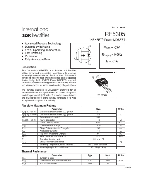
IRF5305HEXFET ® Power MOSFETPD - 91385BFifth Generation HEXFETs from International Rectifier utilize advanced processing techniques to achieve extremely low on-resistance per silicon area. This benefit,combined with the fast switching speed and ruggedized device design that HEXFET Power MOSFETs are well known for, provides the designer with an extremely efficient and reliable device for use in a wide variety of applications.The TO-220 package is universally preferred for all commercial-industrial applications at power dissipation levels to approximately 50 watts. The low thermal resistance and low package cost of the TO-220 contribute to its wide acceptance throughout the industry.ParameterMax.UnitsI D @ T C = 25°C Continuous Drain Current, VGS @ -10V -31ID @ T C = 100°C Continuous Drain Current, V GS @ -10V -22A I DMPulsed Drain Current -110P D @T C = 25°C Power Dissipation 110W Linear Derating Factor 0.71W/°C V GS Gate-to-Source Voltage± 20V E AS Single Pulse Avalanche Energy 280mJ I AR Avalanche Current-16A E AR Repetitive Avalanche Energy 11mJ dv/dt Peak Diode Recovery dv/dt -5.0V/ns T J Operating Junction and-55 to + 175T STGStorage Temperature RangeSoldering Temperature, for 10 seconds 300 (1.6mm from case )°CMounting torque, 6-32 or M3 srew10 lbf•in (1.1N•m)Absolute Maximum RatingsParameterTyp.Max.UnitsR θJC Junction-to-Case––– 1.4R θCS Case-to-Sink, Flat, Greased Surface 0.50–––°C/WR θJAJunction-to-Ambient–––62Thermal Resistancel Advanced Process Technology l Dynamic dv/dt Ratingl 175°C Operating Temperature l Fast Switching l P-ChannellFully Avalanche RatedDescription3/3/00IRF5305IRF5305IRF5305IRF5305IRF5305IRF5305IRF5305。
EDS-510A

MTBF(平均无故障时间): 时间:204,000 小时 数据库:MIL-HDBK-217J,GB 25 ˚C 保修 保修期:5年
尺寸
30.0 mm (1.2 in) 9.0 mm (0.4 in)
15.0 mm (0.6 in) 51.3 mm (2.0 in) 13.9 mm (0.5 in)
RSTP/STP (IEEE 802.1w/D) • IGMP Snooping及GMRP,用来过滤工业以太网协议中的多
播流量 • 基于端口VLAN,IEEE 802.1Q VLAN和GVRP,轻松实现网络
规划
规格
技术参数 标准: IEEE 802.3适用于10BaseT IEEE 802.3u适用于100BaseT(X)和100BaseFX IEEE 802.3ab适用于1000BaseT(X) IEEE 802.3z适用于1000BaseX IEEE 802.3x适用于流量控制 IEEE 802.1D适用于生成树协议 IEEE 802.1w适用于快速生成树协议 IEEE 802.1Q适用于VLAN Tagging IEEE 802.1p适用于Class of Service IEEE 802.1X适用于认证 IEEE 802.3ad适用于基于LACP的端口聚合 协议:IGMPv1/v2,GMRP,GVRP,SNMPv1/v2c/v3,DHCP 服务器/客户端,BootP,TFTP,SNTP,SMTP,RARP,RMON, HTTP,HTTPS,Telnet,Syslog,DHCP Option 66/67/82,SSH, SNMP Inform,Modbus/TCP,LLDP,IEEE 1588 PTP,IPv6
工业自动化完整解决方案
IRF510场效应管

Power MOSFETIRF510, SiHF510Vishay SiliconixFEATURES•Dynamic dV/dt Rating•Repetitive Avalanche Rated •175 °C Operating Temperature •Fast Switching •Ease of Paralleling•Simple Drive Requirements •Lead (Pb)-free AvailableDESCRIPTIONThird generation Power MOSFETs from Vishay provide the designer with the best combination of fast switching,ruggedized device design, low on-resistance and cost-effectiveness.The TO-220 package is universally preferred for all commercial-industrial applications at power dissipation levels to approximately 50 W. The low thermal resistance and low package cost of the TO-220 contribute to its wide acceptance throughout the industry.Notesa.Repetitive rating; pulse width limited by maximum junction temperature (see fig. 11).b.V DD = 25 V, starting T J = 25 °C, L = 4.8 mH, R G = 25 Ω, I AS = 5.6 A (see fig. 12).c.I SD ≤ 5.6 A, dI/dt ≤ 75 A/µs, V DD ≤ V DS , T J ≤ 175 °C.d. 1.6 mm from case.PRODUCT SUMMARYV DS (V)100R DS(on) (Ω)V GS = 10 V0.54Q g (Max.) (nC)8.3Q gs (nC) 2.3Q gd (nC) 3.8ConfigurationSingleTO-220GDSORDERING INFORMATIONPackage TO-220Lead (Pb)-free IRF510PbF SiHF510-E3 SnPbIRF510SiHF510ABSOLUTE MAXIMUM RATINGS T C = 25 °C, unless otherwise notedARAMETER SYMBOL LIMIT UNIT Drain-Source Voltage V DS100VGate-Source Voltage V GS ± 20 Continuous Drain Current V GS at 10 VT C = 25 °C I D5.6A T C = 100 °C4.0Pulsed Drain Current a I DM 20Linear Derating Factor0.29W/°C Single Pulse Avalanche Energy b E AS 100mJ Repetitive Avalanche Current a I AR 5.6 A Repetitive Avalanche Energy a E AR 4.3mJ Maximum Power Dissipation T C = 25 °CP D 43WPeak Diode Recovery dV/dt cdV/dt 5.5V/ns Operating Junction and Storage Temperature Range T J , T stg- 55 to + 175°C Soldering Recommendations (Peak Temperature)for 10 s 300d Mounting Torque6-32 or M3 screw10 lbf · in 1.1N · m * Pb containing terminations are not RoHS compliant, exemptions may apply捷多邦,您值得信赖的PCB打样专家!IRF510, SiHF510Vishay SiliconixNotesa.Repetitive rating; pulse width limited by maximum junction temperature (see fig. 11).b.Pulse width ≤ 300 µs; duty cycle ≤ 2 %.THERMAL RESISTANCE RATINGSARAMETER SYMBOL TY P .MAX.UNITMaximum Junction-to-Ambient R thJA -62°C/W Case-to-Sink, Flat, Greased Surface R thCS 0.50-Maximum Junction-to-Case (Drain)R thJC- 3.5IRF510, SiHF510Vishay Siliconix TYPICAL CHARACTERISTICS 25 °C, unless otherwise notedFig. 1 - Typical Output Characteristics, T C = 25 °C Fig. 2 - Typical Output Characteristics, T C = 175 °CFig. 3 - Typical Transfer Characteristics Fig. 4 - Normalized On-Resistance vs. TemperatureIRF510, SiHF510 Vishay SiliconixFig. 5 - Typical Capacitance vs. Drain-to-Source Voltage Fig. 6 - Typical Gate Charge vs. Gate-to-Source Voltage Fig. 7 - Typical Source-Drain Diode Forward Voltage Fig. 8 - Maximum Safe Operating AreaIRF510, SiHF510Vishay SiliconixFig. 9 - Maximum Drain Current vs. Case TemperatureFig. 10a - Switching Time Test CircuitFig. 10b - Switching Time WaveformsFig. 11 - Maximum Effective Transient Thermal Impedance, Junction-to-CaseFig. 12a - Unclamped Inductive Test CircuitFig. 12b - Unclamped Inductive WaveformsIRF510, SiHF510Vishay SiliconixFig. 12c - Maximum Avalanche Energy vs. Drain CurrentFig. 13a - Basic Gate Charge Waveform Fig. 13b - Gate Charge Test CircuitIRF510, SiHF510Vishay Siliconix Array Fig. 14 - For N-ChannelVishay Siliconix maintains worldwide manufacturing capability. Products may be manufactured at one of several qualified locations. Reliability data for Silicon Technology and Package Reliability represent a composite of all qualified locations. For related documents such as package/tape drawings, part marking, andreliability data, see /ppg?91015.Disclaimer Legal Disclaimer NoticeVishayAll product specifications and data are subject to change without notice.Vishay Intertechnology, Inc., its affiliates, agents, and employees, and all persons acting on its or their behalf (collectively, “Vishay”), disclaim any and all liability for any errors, inaccuracies or incompleteness contained herein or in any other disclosure relating to any product.Vishay disclaims any and all liability arising out of the use or application of any product described herein or of any information provided herein to the maximum extent permitted by law. The product specifications do not expand or otherwise modify Vishay’s terms and conditions of purchase, including but not limited to the warranty expressed therein, which apply to these products.No license, express or implied, by estoppel or otherwise, to any intellectual property rights is granted by this document or by any conduct of Vishay.The products shown herein are not designed for use in medical, life-saving, or life-sustaining applications unless otherwise expressly indicated. Customers using or selling Vishay products not expressly indicated for use in such applications do so entirely at their own risk and agree to fully indemnify Vishay for any damages arising or resulting from such use or sale. Please contact authorized Vishay personnel to obtain written terms and conditions regarding products designed for such applications.Product names and markings noted herein may be trademarks of their respective owners.。
EDS-510A

3.17 x 5.31 x 4.13 in.
重量:1170 g
安装方式:导轨、壁挂(可选套件)
工作环境
操作温度:0 ~ 60 ˚C (32 ~ 140 ˚F)
-40 ~ 75 ˚C (-40 ~ 167 ˚F) (宽温产品)
存储温度:-40 ~ 85 ˚C (-40 ~ 185 ˚F)
周围环境相对湿度:5%~95% (无凝露)
工业以太网完整解决方案
规格
技术参数 标准:IEEE802.3,802.3u,802.3x,802.1D,802.1W, 802.1Q,802.1p,802.1X,802.3ad,802.3z 协议:IGMP V1/V2/V3 device,GMRP,GVRP,SNMP V1/ V2c/V3,DHCP服务器/客户端,DHCP Option 82,BootP, TFTP,SNTP,SMTP,RARP,RMON MIB:MIB-II,Ethernet-Like MIB,P-BRIDGE MIB, Q-BRIDGE MIB,Bridge MIB,RSTP MIB,RMON MIB Group 1,2,3,9 流控:IEEE802.3x 流控,背压式流控 接口 RJ45接口:10/100BaseT(X) or 10/100/1000BaseT(X) 自适 应 光纤接口:Optional 1000BaseSX/LX/LHX/ZX (LC接口) 控制口:RS-232 (RJ45) LED指示灯:PWR1,PWR2,FAULT,10/100M (电口), 1000M (Gigabit口),MASTER,COUPLER 报警输出:两路继电器输出,电流负载能力1A@24 VDC 数字输入:两路数字输入,共地,电气隔离
2-16
/IE e-mail: china@
常用三极管参数大全

玉林万顺达电脑芯片级维修资料 2010-07-20整理玉林万顺达电脑芯片级维修资料 2010-07-20整理玉林万顺达电脑芯片级维修资料 2010-07-20整理玉林万顺达电脑芯片级维修资料 2010-07-20整理玉林万顺达电脑芯片级维修资料 2010-07-20整理玉林万顺达电脑芯片级维修资料 2010-07-20整理玉林万顺达电脑芯片级维修资料 2010-07-20整理玉林万顺达电脑芯片级维修资料 2010-07-20整理玉林万顺达电脑芯片级维修资料 2010-07-20整理玉林万顺达电脑芯片级维修资料 2010-07-20整理玉林万顺达电脑芯片级维修资料 2010-07-20整理玉林万顺达电脑芯片级维修资料 2010-07-20整理玉林万顺达电脑芯片级维修资料 2010-07-20整理玉林万顺达电脑芯片级维修资料 2010-07-20整理玉林万顺达电脑芯片级维修资料 2010-07-20整理玉林万顺达电脑芯片级维修资料 2010-07-20整理玉林万顺达电脑芯片级维修资料 2010-07-20整理玉林万顺达电脑芯片级维修资料 2010-07-20整理玉林万顺达电脑芯片级维修资料 2010-07-20整理玉林万顺达电脑芯片级维修资料 2010-07-20整理玉林万顺达电脑芯片级维修资料 2010-07-20整理玉林万顺达电脑芯片级维修资料 2010-07-20整理玉林万顺达电脑芯片级维修资料 2010-07-20整理玉林万顺达电脑芯片级维修资料 2010-07-20整理玉林万顺达电脑芯片级维修资料 2010-07-20整理玉林万顺达电脑芯片级维修资料 2010-07-20整理玉林万顺达电脑芯片级维修资料 2010-07-20整理玉林万顺达电脑芯片级维修资料 2010-07-20整理玉林万顺达电脑芯片级维修资料 2010-07-20整理玉林万顺达电脑芯片级维修资料 2010-07-20整理。
ILX505A中文资料

Notes) 1) For the sensitivity test light is applied with a uniform intensity of illumination. 2) W lamp (2854K) 3) PRNU is defined as indicated below. Ray incidence conditions are the same as for Note 1.
元器件交易网
ILX505A
2592-pixel CCD Linear Image Sensor (B/W)
For the availability of this product, please contact the sales office.
Description The ILX505A is a reduction type CCD linear sensor
Max. 25.2 — 8.0 — 2.0 3.0 — — — 20.0 10.0 — — —
Unit V/(lx · s) V/(lx · s)
% V mV mV % — lx · s mA mA % Ω V
Remarks Note 1 Note 2 Note 3 — Note 4 Note 4 Note 5 Note 6 Note 7 — — — — Note 8
–1–
E92Y22D78-PS
元器件交易网
Block Diagram
VDD2 NC VDD1 GND GND VDD1 NC NC GND
22
21
20
17
16
15
14
13
12
D14 D15 D33 S1 S2 S2591 S2592 D34 D35 D36 D37 D38 D39
IRF7805中文资料
Source-Drain Rating & Characteristics Parameter Diode Forward Voltage* Reverse Recovery Charge Reverse Recovery Charge (with Parallel Schotkky) Notes:
元器件交易网
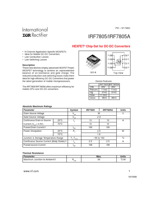
IRF7805/IRF7805A
Power MOSFET Selection for DC/DC Converters
Control FET Special attention has been given to the power losses in the switching elements of the circuit - Q1 and Q2. Power losses in the high side switch Q1, also called the Control FET, are impacted by the Rds(on) of the MOSFET, but these conduction losses are only about one half of the total losses. Power losses in the control switch Q1 are given by;
+ (Qg × Vg × f )
(
2
)
Q Qrr × Vin × f ) + oss × Vin × f + ( 2
*dissipated primarily in Q1.
3
元器件交易网
IRF7805/IRF7805A
For the synchronous MOSFET Q2, Rds(on) is an important characteristic; however, once again the importance of gate charge must not be overlooked since it impacts three critical areas. Under light load the MOSFET must still be turned on and off by the control IC so the gate drive losses become much more significant. Secondly, the output charge Qoss and reverse recovery charge Qrr both generate losses that are transfered to Q1 and increase the dissipation in that device. Thirdly, gate charge will impact the MOSFETs’ susceptibility to Cdv/dt turn on. The drain of Q2 is connected to the switching node of the converter and therefore sees transitions between ground and Vin. As Q1 turns on and off there is a rate of change of drain voltage dV/dt which is capacitively coupled to the gate of Q2 and can induce a voltage spike on the gate that is sufficient to turn the MOSFET on, resulting in shoot-through current . The ratio of Qgd/Qgs1 must be minimized to reduce the potential for Cdv/dt turn on. Spice model for IRF7805 can be downloaded in machine readable format at .
IRF510A中文资料

1005.6Value Units V TO-2201.Gate2. Drain3. Source321DISCLAIMERFAIRCHILD SEMICONDUCTOR RESERVES THE RIGHT TO MAKE CHANGES WITHOUT FURTHER NOTICE TO ANY PRODUCTS HEREIN TO IMPROVE RELIABILITY , FUNCTION OR DESIGN. FAIRCHILD DOES NOT ASSUME ANY LIABILITY ARISING OUT OF THE APPLICATION OR USE OF ANY PRODUCT OR CIRCUIT DESCRIBED HEREIN; NEITHER DOES IT CONVEY ANY LICENSE UNDER ITS PATENT RIGHTS, NOR THE RIGHTS OF OTHERS.TRADEMARKSThe following are registered and unregistered trademarks Fairchild Semiconductor owns or is authorized to use and is not intended to be an exhaustive list of all such trademarks.LIFE SUPPORT POLICYFAIRCHILD S PRODUCTS ARE NOT AUTHORIZED FOR USE AS CRITICAL COMPONENTS IN LIFE SUPPORTDEVICES OR SYSTEMS WITHOUT THE EXPRESS WRITTEN APPROVAL OF FAIRCHILD SEMICONDUCTOR CORPORATION.As used herein:1. Life support devices or systems are devices orsystems which, (a) are intended for surgical implant intothe body, or (b) support or sustain life, or (c) whosefailure to perform when properly used in accordancewith instructions for use provided in the labeling, can be reasonably expected to result in significant injury to the user.2. A critical component is any component of a life support device or system whose failure to perform can be reasonably expected to cause the failure of the life support device or system, or to affect its safety or effectiveness.PRODUCT STATUS DEFINITIONS Definition of Terms Datasheet Identification Product Status DefinitionAdvance InformationPreliminaryNo Identification Needed Obsolete This datasheet contains the design specifications for product development. Specifications may change in any manner without notice.This datasheet contains preliminary data, andsupplementary data will be published at a later date.Fairchild Semiconductor reserves the right to make changes at any time without notice in order to improve design.This datasheet contains final specifications. Fairchild Semiconductor reserves the right to make changes at any time without notice in order to improve design.This datasheet contains specifications on a product that has been discontinued by Fairchild semiconductor.The datasheet is printed for reference information only.Formative or In Design First ProductionFull ProductionNot In ProductionMICROWIRE OPTOLOGIC OPTOPLANAR PACMAN POPPower247 PowerTrench QFET QSQT Optoelectronics Quiet SeriesFAST FASTr FRFETGlobalOptoisolator GTO HiSeC I 2CISOPLANAR LittleFET MicroFET MicroPakRev. H5âACExBottomless CoolFETCROSSVOLT DenseTrench DOMEEcoSPARK E 2CMOS TM EnSigna TM FACTFACT Quiet SeriesSILENT SWITCHER SMART START SPM STAR*POWER StealthSuperSOT -3SuperSOT -6SuperSOT -8SyncFET TinyLogic TruTranslationâââSTAR*POWER is used under licenseUHC UltraFET VCX â。
- 1、下载文档前请自行甄别文档内容的完整性,平台不提供额外的编辑、内容补充、找答案等附加服务。
- 2、"仅部分预览"的文档,不可在线预览部分如存在完整性等问题,可反馈申请退款(可完整预览的文档不适用该条件!)。
- 3、如文档侵犯您的权益,请联系客服反馈,我们会尽快为您处理(人工客服工作时间:9:00-18:30)。
D -PAK
1. Gate
2. Drain
3. Source
1
3
21
2
3
I -PAK
Value Units A V mJ A A V 1005.64206320
TRADEMARKS
ACEx™CoolFET™
CROSSVOLT™E 2CMOS TM FACT™
FACT Quiet Series™FAST ®FASTr™GTO™HiSeC™
The following are registered and unregistered trademarks Fairchild Semiconductor owns or is authorized to use and is not intended to be an exhaustive list of all such trademarks.
LIFE SUPPORT POLICY
FAIRCHILD’S PRODUCTS ARE NOT AUTHORIZED FOR USE AS CRITICAL COMPONENTS IN LIFE SUPPORT
DEVICES OR SYSTEMS WITHOUT THE EXPRESS WRITTEN APPROV AL OF FAIRCHILD SEMICONDUCTOR CORPORA TION.As used herein:
ISOPLANAR™MICROWIRE™POP™
PowerTrench™QS™
Quiet Series™SuperSOT™-3SuperSOT™-6SuperSOT™-8TinyLogic™
1. Life support devices or systems are devices or systems which, (a) are intended for surgical implant into
the body, or (b) support or sustain life, or (c) whose
failure to perform when properly used in accordance
with instructions for use provided in the labeling, can be reasonably expected to result in significant injury to the user.
2. A critical component is any component of a life
support device or system whose failure to perform can be reasonably expected to cause the failure of the life support device or system, or to affect its safety or effectiveness.PRODUCT STATUS DEFINITIONS Definition of Terms Datasheet Identification Product Status Definition
Advance Information
Preliminary No Identification Needed Obsolete This datasheet contains the design specifications for product development. Specifications may change in any manner without notice.
This datasheet contains preliminary data, and
supplementary data will be published at a later date.Fairchild Semiconductor reserves the right to make changes at any time without notice in order to improve design.
This datasheet contains final specifications. Fairchild Semiconductor reserves the right to make changes at any time without notice in order to improve design.
This datasheet contains specifications on a product that has been discontinued by Fairchild semiconductor.The datasheet is printed for reference information only.
Formative or In Design
First Production
Full Production
Not In Production
DISCLAIMER
FAIRCHILD SEMICONDUCTOR RESERVES THE RIGHT TO MAKE CHANGES WITHOUT FURTHER NOTICE TO ANY PRODUCTS HEREIN TO IMPROVE RELIABILITY , FUNCTION OR DESIGN. FAIRCHILD DOES NOT ASSUME ANY LIABILITY ARISING OUT OF THE APPLICATION OR USE OF ANY PRODUCT OR CIRCUIT DESCRIBED HEREIN; NEITHER DOES IT CONVEY ANY LICENSE UNDER ITS PATENT RIGHTS, NOR THE RIGHTS OF OTHERS.
UHC™VCX™。