32位浮点数开平方设计仿真实验报告
vivado cordic ip核计算平方根

Vivado Cordic IP核计算平方根一、背景介绍在数字信号处理领域中,计算平方根是一个非常重要的运算。
在FPGA设计中,使用Cordi c算法来计算平方根是一种非常高效的方法。
Cordic算法是一种迭代算法,可以用于计算三角函数、指数函数、对数函数等。
二、Cordic算法原理Cordic算法是一种旋转算法,它使用一系列的旋转向量将一个向量旋转到另一个向量。
在计算平方根时,我们可以将一个数表示为一个向量(x,0),然后使用Cordic算法将它旋转到向量(1,0),这样就可以得到这个数的平方根。
Cordic算法的核心是旋转向量的选择。
对于计算平方根,我们可以使用以下旋转向量:K(i) = 2^(-i)theta(i) = arctan(2^(-i))在每一次迭代中,我们将向量旋转一个角度theta(i),然后将向量的长度缩小一个因子K(i)。
这样,经过多次迭代,向量就会被旋转到向量(1,0),这时向量的长度就是原数的平方根。
三、Vivado Cordic IP核Vivado是Xilinx公司推出的一款FPGA设计软件,它包含了很多IP核,其中就包括了Cordic IP核。
使用Vivado Cordic IP核来计算平方根非常简单,只需要按照以下步骤操作:1. 打开Vivado软件,创建一个新的工程。
2. 在工程中添加Cordic IP核。
可以在IP目录中找到Cordic IP核,然后将它添加到工程中。
3. 配置Cordic IP核。
在配置界面中,选择计算平方根,并设置输入数据的位宽和精度。
可以选择使用定点数或浮点数进行计算。
4. 运行仿真。
在仿真中,可以输入一个数,然后观察输出结果是否正确。
五、实例演示下面是一个使用Vivado Cordic IP核计算平方根的实例演示。
假设我们要计算数值9的平方根,我们可以按照以下步骤操作:1. 打开Vivado软件,创建一个新的工程。
2. 在工程中添加Cordic IP核。
32位程序 double类型计算处理

标题:32位程序中的double类型计算处理随着计算机科学技术的不断发展,双精度浮点数(double)类型在32位程序中的计算处理成为了关注的焦点之一。
本文将就此话题进行探讨,介绍双精度浮点数在32位程序中的计算处理方法和注意事项。
1. 双精度浮点数的定义和特点双精度浮点数是一种用于表示实数的数据类型,通常占据64位的存储空间,其中52位用于表示尾数,11位用于表示指数,1位用于表示符号位。
这使得双精度浮点数在表示范围和精度上都比单精度浮点数更加优越,因此在科学计算和工程领域得到广泛应用。
2. 双精度浮点数在32位程序中的计算处理双精度浮点数在32位程序中的计算处理需要特别注意,因为在32位系统中,CPU通常只能一次处理32位的数据。
在进行双精度浮点数的计算处理时,需要借助CPU的特殊指令集或者使用软件模拟的方式来完成。
3. 特殊指令集的利用对于支持双精度浮点数计算的32位系统,通常会提供一些特殊的指令集来加速双精度浮点数的计算处理。
Intel的SSE(Streaming SIMD Extensions)指令集就提供了对双精度浮点数进行快速计算的指令,可以大大提高计算速度。
4. 软件模拟的处理方法对于不支持双精度浮点数计算的32位系统,可以通过软件模拟的方式来实现双精度浮点数的计算处理。
这种方法虽然速度较慢,但可以在不支持硬件加速的系统上实现双精度浮点数的计算。
5. 精度和舍入误差的问题双精度浮点数的计算处理中,由于计算机内部二进制表示和十进制实数的差异,常常会出现精度损失和舍入误差。
因此在对双精度浮点数进行计算处理时,需要特别注意精度问题,避免因为舍入误差而影响计算结果的准确性。
6. 结论在32位程序中进行双精度浮点数的计算处理,需要结合特殊指令集和软件模拟的方法来实现。
同时要注意精度和舍入误差的问题,保证计算结果的准确性。
希望本文能够对读者有所帮助,谢谢!通过以上的内容,应该可以帮助你写出一篇高质量的、流畅易读的文章。
基于FPGA的32位浮点运算单元的设计及其VHDL代码的MATLAB验证.(IJIEEB-V6-N1-1)
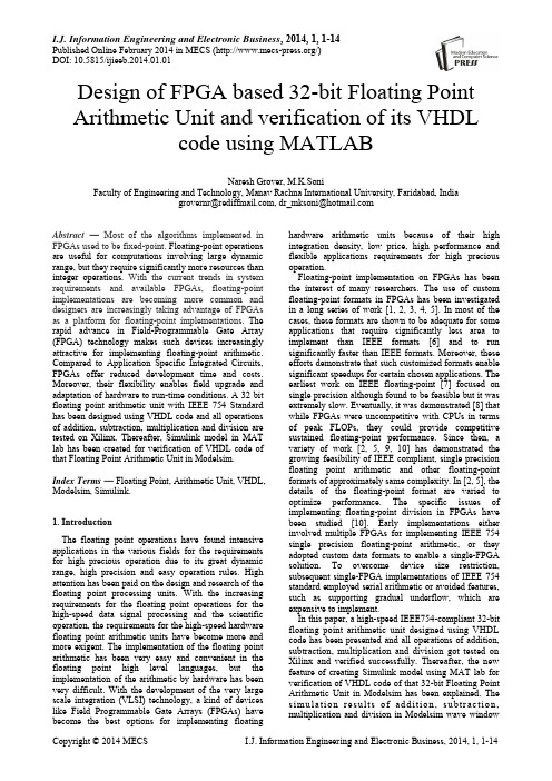
I.J. Information Engineering and Electronic Business, 2014, 1, 1-14Published Online February 2014 in MECS (/)DOI: 10.5815/ijieeb.2014.01.01Design of FPGA based 32-bit Floating Point Arithmetic Unit and verification of its VHDLcode using MATLABNaresh Grover, M.K.SoniFaculty of Engineering and Technology, Manav Rachna International University, Faridabad, Indiagrovernr@, dr_mksoni@Abstract —Most of the algorithms implemented in FPGAs used to be fixed-point. Floating-point operations are useful for computations involving large dynamic range, but they require significantly more resources than integer operations.With the current trends in system requirements and available FPGAs, floating-point implementations are becoming more common and designers are increasingly taking advantage of FPGAs as a platform for floating-point implementations. The rapid advance in Field-Programmable Gate Array (FPGA) technology makes such devices increasingly attractive for implementing floating-point arithmetic. Compared to Application Specific Integrated Circuits, FPGAs offer reduced development time and costs. Moreover, their flexibility enables field upgrade and adaptation of hardware to run-time conditions. A 32 bit floating point arithmetic unit with IEEE 754 Standard has been designed using VHDL code and all operations of addition, subtraction, multiplication and division are tested on Xilinx. Thereafter, Simulink model in MAT lab has been created for verification of VHDL code of that Floating Point Arithmetic Unit in Modelsim.Index Terms—Floating Point, Arithmetic Unit, VHDL, Modelsim, Simulink.1. IntroductionThe floating point operations have found intensive applications in the various fields for the requirements for high precious operation due to its great dynamic range, high precision and easy operation rules. High attention has been paid on the design and research of the floating point processing units. With the increasing requirements for the floating point operations for the high-speed data signal processing and the scientific operation, the requirements for the high-speed hardware floating point arithmetic units have become more and more exigent. The implementation of the floating point arithmetic has been very easy and convenient in the floating point high level languages, but the implementation of the arithmetic by hardware has been very difficult. With the development of the very large scale integration (VLSI) technology, a kind of devices like Field Programmable Gate Arrays (FPGAs) have become the best options for implementing floating hardware arithmetic units because of their high integration density, low price, high performance and flexible applications requirements for high precious operation.Floating-point implementation on FPGAs has been the interest of many researchers. The use of custom floating-point formats in FPGAs has been investigated in a long series of work [1, 2, 3, 4, 5]. In most of the cases, these formats are shown to be adequate for some applications that require significantly less area to implement than IEEE formats [6] and to run significantly faster than IEEE formats. Moreover, these efforts demonstrate that such customized formats enable significant speedups for certain chosen applications. The earliest work on IEEE floating-point [7] focused on single precision although found to be feasible but it was extremely slow. Eventually, it was demonstrated [8] that while FPGAs were uncompetitive with CPUs in terms of peak FLOPs, they could provide competitive sustained floating-point performance. Since then, a variety of work [2, 5, 9, 10] has demonstrated the growing feasibility of IEEE compliant, single precision floating point arithmetic and other floating-point formats of approximately same complexity. In [2, 5], the details of the floating-point format are varied to optimize performance. The specific issues of implementing floating-point division in FPGAs have been studied [10]. Early implementations either involved multiple FPGAs for implementing IEEE 754 single precision floating-point arithmetic, or they adopted custom data formats to enable a single-FPGA solution. To overcome device size restriction, subsequent single-FPGA implementations of IEEE 754 standard employed serial arithmetic or avoided features, such as supporting gradual underflow, which are expensive to implement.In this paper, a high-speed IEEE754-compliant 32-bit floating point arithmetic unit designed using VHDL code has been presented and all operations of addition, subtraction, multiplication and division got tested on Xilinx and verified successfully. Thereafter, the new feature of creating Simulink model using MAT lab for verification of VHDL code of that 32-bit Floating Point Arithmetic Unit in Modelsim has been explained. The si mu lat io n r esu lts o f ad d itio n, su b tr actio n, multiplication and division in Modelsim wave windowhave been demonstrated.The rest of the paper is organized as follows. Section 2 presents the general floating point architecture. Section 3 explains the algorithms used to write VHDL codes for implementing 32 bit floating point arithmetic operations: addition/subtraction, multiplication and division. The Section 4 of the paper details the VHDL code and behaviour model for all above stated arithmetic operation. The section 5 explains the design steps along with experimental method to create Simulink model in MAT lab for verification of VHDL code in Modelsim and the results are shown and discussed in its section 6 while section 7 concludes the paper with further scope of work.2. Floating Point ArchitectureFloating point numbers are one possible way of representing real numbers in binary format; the IEEE 754 [11] standard presents two different floating point formats, Binary interchange format and Decimal interchange format. This paper focuses only on single precision normalized binary interchange format. Figure 1 shows the IEEE 754 single precision binary format representation; it consists of a one bit sign (S), an eight bit exponent (E), and a twenty three bit fraction (M) or Mantissa.32 bit Single Precision Floating Point Numbers IEEE standard are stored as:S EEEEEEEE MMMMMMMMMMMMMMMMMMMMMMS: Sign – 1 bitE: Exponent – 8 bitsM: Mantissa – 23 bits Fraction32 bitsFigure.1: IEEE 754 single precision binary format representation The value of number V:If E=255 and F is nonzero, then V= Nan ("Not a Number")If E=255 and F is zero and S is 1, then V= - InfinityIf E=255 and F is zero and S is 0, then V= InfinityIf 0<E<255 then V= (-1) **S * 2 ** (E-127) * (1.F) (exponent range = -127 to +128)If E=0 and F is nonzero, then V= (-1) **S * 2 ** (-126) * (0.F) ("un-normalized" values”)If E=0 and F is zero and S is 1, then V= - 0If E=0 and M is zero and S is 0, then V = 0An extra bit is added to the mantissa to form what is called the significand. If the exponent is greater than 0 and smaller than 255, and there is 1 in the MSB of the significand then the number is said to be a normalized number; in this case the real number is represented by (1)V = (-1s) * 2 (E - Bias) * (1.M) (1)Where M = m22 2-1+ m21 2-2+ m20 2-3+…+ m1 2-22+m0 2-23; Bias = 127.3. Algorithms for Floating Point Arithmetic UnitThe algorithms using flow charts for floating point addition/subtraction, multiplication and division have been described in this section, that become the base for writing VHDL codes for implementation of 32-bit floating point arithmetic unit.3.1 Floating Point Addition / SubtractionThe algorithm for floating point addition is explained through flow chart in Figure 2. While adding the two floating point numbers, two cases may arise. Case I: when both the numbers are of same sign i.e. when both the numbers are either +ve or –ve. In this case MSB of both the numbers are either 1 or 0. Case II: when both the numbers are of different sign i.e. when one number is +ve and other number is –ve. In this case the MSB of one number is 1 and other is 0.Case I: - When both numbers are of same signStep 1:- Enter two numbers N1 and N2. E1, S1 and E1, S2 represent exponent and significand of N1 and N2 respectively.Step 2:- Is E1 or E2 =‟0‟. If yes; set hidden bit of N1 or N2 is zero. If not; then check if E2 > E1, if yes swap N1 and N2 and if E1 > E2; contents of N1 and N2 need not to be swapped.Step 3:- Calculate difference in exponents d=E1-E2. If d = …0‟ then there is no need of shifting the significand. If d is more than …0‟ say …y‟ then shift S2 to the right by an amount …y‟ and fill the left most bits by zero. Sh ifting is done with hidden bit.Step 4:- Amount of shifting i.e. …y‟ is added to exponent of N2 value. New exponent value of E2= (previous E2) + …y‟. Now result is in normalize form because E1 = E2. Step 5:- Check if N1 and N2 have different sign, if …no‟; Step 6:- Add the significands of 24 bits each including hidden bit S=S1+S2.Step 7:- Check if there is carry out in significand addition. If yes; then add …1‟ to the exponent value of either E1 or new E2. After addition, shift the overall result of significand addition to the right by one by making MSB of S as …1‟ a nd dropping LSB of significand.Step 8:- If there is no carry out in step 6, then previous exponent is the real exponent.Step 9:- Sign of the result i.e. MSB = MSB of either N1 or N2.Step 10:- Assemble result into 32 bit format excluding 24th bit of significand i.e. hidden bit.Case II: - When both numbers are of different sign Step 1, 2, 3 & 4 are same as done in case I.Step 5:- Check if N1 and N2 have different sign, if …Yes‟;Step 6:- Take 2‟s complement of S2 and then add it to S1 i.e. S=S1+ (2‟s co mplement of S2).Step 7:- Check if there is carry out in significand addition. If yes; then discard the carry and also shift the result to left until there is …1‟ in MSB and also count the amount of shifting say …z‟.Step 8:- Subtract …z‟ from exponent val ue either from E1 or E2. Now the original exponent is E1-…z‟. Also append the …z‟ amount of zeros at LSB.Step 9:- If there is no carry out in step 6 then MSB must be …1‟ and in this case simply replace …S‟ by 2‟s complement.Step 10:- Sign of the result i.e. MSB = Sign of the larger number either MSB of N1or it can be MSB of N2. Step 11:- Assemble result into 32 bit format excluding 24th bit of significand i.e. hidden bit.Figure. 2: Flow Chart for floating point Addition/SubtractionIn this algorithm three 8-bit comparators, one 24-bit and two 8-bit adders, two 8-bit subtractors, two shift units and one swap unit are required in the design.First 8-bit comparator is used to compare the exponent of two numbers. If exponents of two numbers are equal then there is no need of shifting. Second 8-bit comparator compares exponent with zero. If the exponent of any number is zero set the hidden bit of that number zero. Third comparator is required to check whether the exponent of number 2 is greater than number 1. If the exponent of number 2 is greater than number 1 then the numbers are swapped.One subtractor is required to compute the difference between the 8-bit exponents of two numbers. Second subtractor is used if both the numbers are of different sign than after addition of the significands of two numbers if carry appears. This carry is subtracted from the exponent using 8-bit subtractor.One 24-bit adder is required to add the 24-bit significands of two numbers. One 8-bit adder is required if both the numbers are of same sign than after addition of the significands of two numbers if carry appears. This carry is added to the exponent using 8-bit adder. Second 8-bit adder is used to add the amount of shifting to the exponent of smaller number.One swap unit is required to swap the numbers if N2 is greater than N1. Swapping is normally done by taking the third variable. Two shift units are required one is shift left and second is shift right.3.2 Floating Point MultiplicationThe algorithm for floating point multiplication is explained through flow chart in Figure 3. Let N1 and N2 are normalized operands represented by S1, M1, E1 and S2, M2, E2 as their respective sign bit, mantissa (significand) and exponent. Basically following four steps are used for floating point multiplication.1. Multiply signifcands, add exponents, and determine signM=M1*M2E=E1+E2-BiasS=S1XORS22. Normalize Mantissa M (Shift left or right by 1) and update exponent E3. Rounding the result to fit in the available bits4. Determine exception flags and special values for overflow and underflow.Figure. 3: Flow Chart for floating point MultiplicationSign Bit Calculation: The result of multiplication is a negative sign if one of the multiplied numbers is of a negative value and that can be obtained by XORing the sign of two inputs.Exponent Addition is done through unsigned adder for adding the exponent of the first input to the exponent of the second input and after that subtract the Bias (127) from the addition result (i.e. E1+E2 - Bias). The result of this stage can be called as intermediate exponent. Significand Multiplication is done for multiplying the unsigned significand and placing the decimal point in the multiplication product. The result of significand multiplication can be called as intermediate product (IP). The unsigned significand multiplication is done on 24 bit.The result of the significand multiplication (intermediate product) must be normalized to have a leading …1‟ just to the left of the decimal point (i.e. in the bit 46 in the intermediate product). Since the inputs are normalized numbers then the intermediate product has the leading one at bit 46 or 47. If the leading one is at bit 46 (i.e. to the left of the decimal point) then the intermediate product is already a normalized number and no shift is needed. If the leading one is at bit 47 then the intermediate product is shifted to the right and the exponent is incremented by 1.Overflow/underflow means that the result‟s exponent is too large/small to be represented in the exponent field. Themust be between 1 and 254 otherwise the value is not anormalized one .An overflow may occur while adding the two exponents or during normalization. Overflow due to exponent addition can be compensated during subtraction of the bias; resulting in a normal output value (normal operation). An underflow may occur while subtracting the bias to form the intermediate exponent. If the intermediate exponent < 0 then it is an underflow that can never be compensated; if the intermediate exponent = 0 then it is an underflow that may be compensated during normalization by adding 1 to it .When an overflow occurs an overflow flag signal goes high and the result turns to ±Infinity (sign determined according to the sign of the floating point multiplier inputs). When an underflow occurs an underflow flag signal goes high and the result turns to ±Zero (sign determined according to the sign of the floating point multiplier inputs). 3.3 Floating Point DivisionThe algorithm for floating point multiplication is explained through flow chart in Figure 4. Let N1 and N2 are normalized operands represented by S1, M1, E1 and S2, M2, E2 as their respective sign bit, mantissa (significand) and exponent. If let us say we consider x=N1 and d=N2 and the final result q has been taken as “x/d”. Again the following four steps are used for floating point division.Figure. 4: Flow Chart for floating point Division (q = x/d; N1=x and N2=d)1. Divide signifcands, subtract exponents, and determine signM=M1/M2E=E1-E2S=S1XORS22. Normalize Mantissa M (Shift left or right by 1) and update exponent E3. Rounding the result to fit in the available bits4. Determine exception flags and special valuesThe sign bit calculation, mantissa division, exponent subtraction (no need of bias subtraction here), rounding the result to fit in the available bits and normalization is done in the similar way as has been described for multiplication.4. VHDL CodeThis section illustrates the main steps of VHDL code that has been used to implement the 32-bit floating point arithmetic functions: addition/subtraction, multiplication and division. It includes the arithmetic structure followed by behavior model for different arithmetic functions for 32-bit floating point format following IEEE 754 standards.ARITHMETIC UNIT STRUCTUREentity fp_alu isport(in1,in2:in std_logic_vector(31 downto 0);clk:in std_logic;sel:in std_logic_vector(1 downto 0);output1:out std_logic_vector(31 downto 0));end fp_alu;architecture fp_alu_struct of fp_alu iscomponent divider isport(clk : in std_logic;res : in std_logic;GO : in std_logic;x : in std_logic_vector(31 downto 0);y : in std_logic_vector(31 downto 0);z : out std_logic_vector(31 downto 0);done : out std_logic;overflow : out std_logic);end component;component fpa_seq isport(n1,n2:in std_logic_vector(32 downto 0);clk:in std_logic;sum:out std_logic_vector(32 downto 0));end component;component fpm isport(in1,in2:in std_logic_vector(31 downto 0);out1:out std_logic_vector(31 downto 0));end component;signal out_fpa: std_logic_vector(32 downto 0);signal out_fpm,out_div: std_logic_vector(31 downto 0); signal in1_fpa,in2_fpa: std_logic_vector(32 downto 0); beginin1_fpa<=in1&'0';in2_fpa<=in2&'0';fpa1:fpa_seq port map(in1_fpa,in2_fpa,clk,out_fpa); fpm1:fpm port map(in1,in2,out_fpm);fpd1:divider port map(clk,'0','1',in1,in2,out_div); process(sel,clk)beginif(sel="01")thenoutput1<=out_fpa(32 downto 1);elsif(sel="10")thenoutput1<=out_fpm;elsif(sel="11")thenoutput1<=out_div;end if;end process;end fp_alu_struct;FPA BEHAVIOURentity fpa_seq isport(n1,n2:in std_logic_vector(32 downto 0);clk:in std_logic;sum:out std_logic_vector(32 downto 0));end fpa_seq;architecture Behavioral of fpa_seq is--signal f1,f2:std_logic_vector(23 downto0):="000000000000000000000000";signal sub_e:std_logic_vector(7 downto0):="00000000";--signal addi:std_logic_vector(34 downto 0);signal c_temp:std_logic:='0';--_vector(34 downto 0); signal shift_count1:integer:=0;signal num2_temp2: std_logic_vector(32 downto 0):="000000000000000000000000000000000"; signal s33:std_logic_vector(23 downto0):="000000000000000000000000";signal s2_temp :std_logic_vector(23 downto0):="000000000000000000000000";signal diff:std_logic_vector(7 downto 0):="00000000"; ----------sub calling-----------------------------------------------------------------sub(e1,e2,d);if(d>="00011100")thensum<=num1;elsif(d<"00011100")thenshift_count:=conv_integer(d);shift_count1<=shift_count;num2_temp2<=num2;--s2_temp<=s2;--------------shifter calling---------------------------------------------------------shift(s2,shift_count,s3);--s33<=s3;------------sign bit checking------if (num1(32)/=num2(32))thens3:=(not(s3)+'1');------2's complementadder23(s1,s3,s4,c_out);if(c_out='1')thenshift_left(s4,d_shl,ss4);sub(e1,d_shl,ee4);sum<=n1(32)& ee4 & ss4;elseif(s4(23)='1')thens4:=(not(s4)+'1');------2's complementsum<=n1(32)& e1 & ss4;end if;end if; elses3:=s3;-- end if;---------------------same sign start---------------adder 8 calling--------------- adder8(e2,d,e3);sub_e<=e3;num1_temp:=n1(32)& e1 & s1;num2_temp:=n2(32)& e3 & s3;---------------adder 23 calling--------------- adder23(s1,s3,s4,c_out);--s2_temp<=s4;c_temp<=c_out;if(c_out='1')then--shift1(s4,s_1,s5);--s2_temp<=s5;s33<=s4;s5:='1' & s4(23 downto 1);s2_temp<=s5;adder8(e3,"00000001",e4);e3:=e4;--sub_e<=e4;sum<=n1(32)& e3 & s5;elsesum<=n1(32)& e3 & s4;end if;end if;end if;end if;----same sign endend if;------final result assembling------------sum_temp<=n1(32)& e1 & s4;--sum<=n1(32)& e3 & s4;end process;end Behavioral;FPM BEHAVIOURentity fpm isport(in1,in2:in std_logic_vector(31 downto 0);out1:out std_logic_vector(31 downto 0));end fpm;architecture Behavioral of fpm isprocedure adder( a,b:in std_logic_vector(7 downto 0); sout : out STD_LOGIC_VECTOR (8 downto 0))isvariable g,p:std_logic_vector(7 downto 0);variable c:std_logic_vector(8 downto 0);variable sout1 :STD_LOGIC_VECTOR (7 downto 0); beginc(0):='0';for i in 0 to 7 loopg(i):= a(i) and b(i);p(i):= a(i) xor b(i);end loop;for i in 0 to 7 loopc(i+1):=(g(i) or (c(i) and p(i)));end loop;for i in 0 to 7 loopsout1(i):=c(i) xor a(i) xor b(i);end loop;sout:=c(8) & sout1;end adder;-------------------------------------------multiplier-------------------------------procedure multiplier ( a,b : in STD_LOGIC_VECTOR (23 downto 0);y : out STD_LOGIC_VECTOR (47 downto 0))is variable temp,prod:std_logic_vector(47 downto 0); begintemp:="000000000000000000000000"&a;prod:="000000000000000000000000000000000000000 000000000";for i in 0 to 23 loopif b(i)='1' thenprod:=prod+temp;end if;temp:=temp(46 downto 0)&'0';end loop;y:=prod;end multiplier; --------------------------end multipier-----------------------------------------------beginprocess(in1,in2)variable sign_f,sign_in1,sign_in2: std_logic:='0'; variable e1,e2: std_logic_vector(7 downto0):="00000000";variable add_expo:std_logic_vector(8 downto0):="000000000";variable m1,m2: std_logic_vector(23 downto0):="000000000000000000000000";variable mantisa_round: std_logic_vector(22 downto 0):="00000000000000000000000";variable prod:std_logic_vector(47 downto0):="00000000000000000000000000000000000000000 0000000";variable mul_mantisa :std_logic_vector(47 downto 0):="00000000000000000000000000000000000000000 0000000";variable bias:std_logic_vector(8 downto0):="001111111";variable bias_sub:std_logic_vector(7 downto0):="00000000";variable inc_bias:std_logic_vector(8 downto0):="000000000";variable bias_round:std_logic_vector(8 downto0):="000000000";beginsign calculationsign_in1:=in1(31);sign_in2:=in2(31);sign_f:=sign_in1 xor sign_in2;FPD BEHAVIOURentity divider isport(clk : in std_logic;res : in std_logic;GO : in std_logic;x : in std_logic_vector(31 downto 0);y : in std_logic_vector(31 downto 0);z : out std_logic_vector(31 downto 0);done : out std_logic;overflow : out std_logic);end divider;architecture design of divider issignal x_reg : std_logic_vector(31 downto 0);signal y_reg : std_logic_vector(31 downto 0);signal x_mantissa : std_logic_vector(23 downto 0); signal y_mantissa : std_logic_vector(23 downto 0); signal z_mantissa : std_logic_vector(23 downto 0); signal x_exponent : std_logic_vector(7 downto 0); signal y_exponent : std_logic_vector(7 downto 0); signal z_exponent : std_logic_vector(7 downto 0); signal x_sign : std_logic;signal y_sign : std_logic;signal z_sign : std_logic;signal sign : std_logic;signal SC : integer range 0 to 26;signal exp : std_logic_vector(9 downto 0);signal EA : std_logic_vector(24 downto 0);signal B : std_logic_vector(23 downto 0);signal Q : std_logic_vector(24 downto 0);type states is (reset, idle, s0, s1, s2, s3, s4);signal state : states;beginx_mantissa <= '1' & x_reg(22 downto 0);x_exponent <= x_reg(30 downto 23);x_sign <= x_reg(31);y_mantissa <= '1' & y_reg(22 downto 0);y_exponent <= y_reg(30 downto 23);y_sign <= y_reg(31);process(clk)beginif clk'event and clk = '1' thenif res = '1' thenstate <= reset;exp <= (others => '0');sign <= '0';x_reg <= (others => '0');y_reg <= (others => '0');z_sign <= '0'; z_mantissa <= (others => '0');z_exponent <= (others => '0');EA <= (others => '0');Q <= (others => '0');B <= (others => '0');overflow <= '0';done <= '0';elsecase state iswhen reset => state <= idle;when idle =>if GO = '1' thenstate <= s0;x_reg <= x;y_reg <= y;end if;when s0 => state <= s1;overflow <= '0';SC <= 25;done <= '0';sign <= x_sign xor y_sign;EA <= '0' & x_mantissa;B <= y_mantissa;Q <= (others => '0');exp <= ("00" & x_exponent) + not ("00" & y_exponent) + 1 + "0001111111";when s1 => if (y_mantissa = x"800000" andy_exponent = x"00") thenoverflow <= '1';z_sign <= sign;z_mantissa <= (others => '0');z_exponent <= (others => '1');done <= '1';state <= idle;elsif exp(9) = '1' or exp(7 downto 0) = x"00" or(x_exponent = x"00" and x_mantissa = x"00") or(y_exponent = x"FF" and y_mantissa = x"00") then z_sign <= sign;z_mantissa <= (others => '0');z_exponent <= (others => '0');done <= '1';state <= idle;elseEA <= EA + ('0' & not B) + 1;state <= s2;end if;when s2 =>if EA(24) = '1' thenQ(0) <= '1';elseQ(0) <= '0';EA <= EA + B;end if;SC <= SC - 1;state <= s3;when s3 => if SC = 0 thenif Q(24) = '0' thenQ <= Q (23 downto 0) & '0';exp <= exp - 1;end if;state <= s4;elseEA <= EA(23 downto 0) & Q(24); Q <= Q(23 downto 0) & '0';state <= s1; end if;when s4 => if exp = x"00" thenz_sign <= sign;z_mantissa <= (others => '0');z_exponent <= (others => '0');elsif exp(9 downto 8) = "01" thenz_sign <= sign;z_mantissa <= (others => '0');z_exponent <= (others => '1');elsez_sign <= sign;z_mantissa <= Q(24 downto 1);z_exponent <= exp(7 downto 0);end if;done <= '1';state <= idle;end case;end if;end if;end process;z <= z_sign & z_exponent & z_mantissa(22 downto 0); end design;The VHDL code written has been tested and verified on Xilinx ISE 8.1i for all operation. The design utilization summary has been shown in Figure 5.Figure. 5: Design Utilization Summary of Floating Point Arithmetic Unit on FPGA5. Generation and verification of HDL code using MATLABGeneration and verification of HDL code using MATLAB requires compatible versions of MATLAB (Simulink) and HDL Simulator …Modelsim‟ to be loaded on the same system [13, 14, 15]. The basic design steps to create Simulink model for verification of VHDL code in Modelsim HDL Simulator is shown in the flow chart of Fig. 6.Figure. 6: Design steps to create Simulink model for verification ofVHDL code in ModelsimThe Simulink Model to generate and verify Floating Point arithmetic created is shown in Figure 7. Input 1 and Input 2 are the two 32 bit floating point inputs to the model and …Select‟ is set to …01‟ for Adder, …11‟ for Divider and …10‟ for Multiplier. It also has a scope to view the output. A sub-system is created to launch the Modelsim Simulator from Simulink as shown in Fig. 8.Figure. 7: Simulink model to generate and verify Floating PointarithmeticFigure. 8: Simulink sub-system to launch HDL Simulator6. RESULTSDouble clicking the …Launch HDL Simulator‟ in the Simulink model loads the test bench for simulation. The ModelSim Simulator opens a display window for monitoring the simulation as the test bench runs. The wave window in Figure 9 shows the simulation of two exponential inputs and Select set to …01‟for …adder‟ result as HDL waveform. Figure 10 shows the simulation of two decimal inputs for …adder‟. Figure 11 and 12 show the simulation of two decimal inputs for …divider‟. Figure 13 and 14 show the simulation of two decimal inputs for …multiplier‟.。
计算机32位浮点数编码实验C描述

浮点数编码实验1、提要本篇讲解浮点数的编码,先介绍浮点数的编码规格,最后用C程序来实现将给定的整数编码转换成浮点数编码。
2、浮点数编码在计算机中浮点数采用V = (-1)s×M×2E的形式来表示,在计算机中单精度浮点数是32位,双精度浮点数是64位,我们仅仅对单精度浮点数做说明。
就单精度浮点数而言,计算机中保存了S,M和E 的编码,其中S表示符号位,0表示正数,1表示负数;M是学名叫尾数;E是阶码,它是指数加上一个偏置数,单精度浮点数的偏置数是127,之所以加上这个偏置数是为了便于浮点数的运算。
在单精度浮点数中,符号位占最高位1位,阶码占用紧接着的8位,尾数占用最后23位,如下图所示:31 30 22 0 重点说一下尾数M,M隐含了小数点前面的1,举个例子,如果M是1010000000000011110000B,那么M的实际值是1#1010000000000011110000B,其中#表示小数点的位置;然后说说阶码E,假定解码E是10001001B,十进制值位137,E需要再减去偏置127,才能得到指数137-127=10,最后假定S是0,那么这个例子中所描述的浮点数表示的值是:1.1010000000000011110000B × 210也就是:11010000000.000011110000B。
3、将一个十进制数转成浮点数表示举个例子,十进制数-12.75转换成浮点数表示,首先确定符号位是1,将12.75转成二进制表示1100.11B = 1.10011×23,可以确定尾数M是100 1100 0000 0000 0000 0000B,阶码E=3+127 = 130 = 1000 0010B,其浮点数表示为1#1000 0010#100 1100 0000 0000 0000 0000B =C14C0000H。
其中#分割S、E和M。
4、一些非规格浮点数的表示上面部分说的是浮点数的规格表示,还有一些非规格表示。
32位浮点乘法器的设计与仿真代码

32位浮点乘法器的设计与仿真代码一、引言随着计算机科学和技术的不断发展,浮点乘法器在科学计算、图像处理、人工智能等领域中扮演着重要的角色。
本文将详细讨论32位浮点乘法器的设计与仿真代码,并深入探讨其原理和实现方法。
二、浮点数表示在开始设计32位浮点乘法器之前,我们首先需要了解浮点数的表示方法。
浮点数由符号位、阶码和尾数组成,其中符号位表示数的正负,阶码确定数的大小范围,尾数表示数的精度。
三、浮点乘法器的原理浮点乘法器的原理基于乘法运算的基本原理,即将两个数的尾数相乘,并将阶码相加得到结果的阶码。
同时需要考虑符号位的处理和对阶的操作。
下面是32位浮点乘法器的基本原理:1.获取输入的两个浮点数A和B,分别提取出符号位、阶码和尾数。
2.将A和B的尾数相乘,得到乘积P。
3.将A和B的阶码相加,得到结果的阶码。
4.对乘积P进行规格化,即将小数点左移或右移,使其满足规定的位数。
5.对结果的阶码进行溢出判断,若溢出则进行相应的处理。
6.将符号位与结果的阶码和尾数合并,得到最终的浮点乘积。
四、浮点乘法器的设计根据浮点乘法器的原理,我们可以开始进行浮点乘法器的设计。
设计的关键是确定乘法器中各个部件的功能和连接方式。
下面是浮点乘法器的设计要点:1.输入模块:负责接收用户输入的两个浮点数,并提取出符号位、阶码和尾数。
2.乘法模块:负责将两个浮点数的尾数相乘,得到乘积P。
3.加法模块:负责将两个浮点数的阶码相加,得到结果的阶码。
4.规格化模块:负责对乘积P进行规格化操作,使其满足规定的位数。
5.溢出判断模块:负责判断结果的阶码是否溢出,并进行相应的处理。
6.输出模块:负责将符号位、阶码和尾数合并,得到最终的浮点乘积。
五、浮点乘法器的仿真代码为了验证浮点乘法器的设计是否正确,我们需要进行仿真测试。
下面是一段简单的浮点乘法器的仿真代码:module floating_point_multiplier(input wire [31:0] a,input wire [31:0] b,output wire [31:0] result);wire [31:0] mantissa;wire [7:0] exponent;wire sign;// 提取符号位assign sign = a[31] ^ b[31];// 提取阶码assign exponent = a[30:23] + b[30:23];// 尾数相乘assign mantissa = a[22:0] * b[22:0];// 规格化assign {result[30:23], result[22:0]} = {exponent, mantissa};// 处理溢出always @(*)beginif (exponent > 255)result = 32'b0; // 结果溢出为0else if (exponent < 0)result = 32'b0; // 结果溢出为0elseresult[31] = sign;endendmodule六、浮点乘法器的应用浮点乘法器在科学计算、图像处理、人工智能等领域中有着广泛的应用。
32位浮点加法器设计

32位浮点加法器设计一、基本原理浮点数加法运算是在指数和尾数两个部分进行的。
浮点数一般采用IEEE754标准表示,其中尾数部分采用规格化表示。
浮点加法的基本原理是将两个浮点数的尾数对齐并进行加法运算,再进行规格化处理。
在加法运算过程中,还需考虑符号位、指数溢出、尾数对齐等特殊情况。
二、设计方案1. 硬件实现方案:采用组合逻辑电路实现浮点加法器,以保证运算速度和实时性。
采用Kogge-Stone并行加法器、冒泡排序等技术,提高运算效率。
2.数据输入:设计32位浮点加法器,需要提供两个浮点数的输入端口,包括符号位、指数位和尾数位。
3.数据输出:设计32位浮点加法器的输出端口,输出相加后的结果,包括符号位、指数位和尾数位。
4.控制信号:设计合适的控制信号,用于实现指数对齐、尾数对齐、规格化等操作。
5.流程控制:设计合理的流程控制,对各个部分进行并行和串行处理,提高加法器的效率。
三、关键技术1. Kogge-Stone并行加法器:采用Kogge-Stone并行加法器可以实现多位数的并行加法运算,提高运算效率。
2.浮点数尾数对齐:设计浮点加法器需要考虑浮点数尾数的对齐问题,根据指数大小进行右移或左移操作。
3.溢出判断和处理:浮点加法器需要判断浮点数的指数是否溢出,若溢出需要进行调整和规格化。
4.符号位处理:设计浮点加法器需要考虑符号位的处理,确定加法结果的符号。
四、性能评价性能评价是衡量浮点加法器设计好坏的重要指标。
主要从以下几个方面进行评价:1.精度:通过与软件仿真结果进行比较,评估加法器的运算精度,误差较小的加法器意味着更高的性能。
2.速度:评估加法器的运行速度,主要考虑延迟和吞吐量。
延迟越低,意味着加法器能够更快地输出结果;吞吐量越高,意味着加法器能够更快地处理多个浮点加法运算。
3.功耗:评估加法器的功耗情况,低功耗设计有助于提高整个系统的能效。
4.面积:评估加法器的硬件资源占用情况,面积越小意味着设计更紧凑,可用于片上集成、嵌入式系统等场景。
基于FPGA单精度浮点数算术运算系统的设计与仿真

Electronic Technology •电子技术Electronic Technology & Software Engineering 电子技术与软件工程• 113●基金项目:广西自然科学基金项目(2014GXNSFAA118392);广西教育厅科研项目(YB2014209)。
【关键词】FPGA 单精度浮点运算 模块化 系统FPGA 近年来在体系结构、技术水平和持续改进的设计方面进行了提高和完善,弥补了专用处理器灵活性不足之处,FPGA 的容量、速度和资源已经有了更好的提高。
在微处理器的指令系统中,浮点数加/减和乘/除法指令都是实现2个单精度浮点数的运算,浮点数算术运算系统的设计通常采用流水线和自顶向下方式,但对于所执行的浮点数算术运算指令需要应用上一条运算指令的运算结果作为操作数的指令,则浮点数算术运算的流水线操作失去作用,影响了浮点数算术运算指令执行的速度。
本设计利用Verilog 语言,采用基于FPGA 自主设计的浮点数算术运算系统,进行浮点加减乘除运算验证和仿真,提高了运算的操作速度,具有较强的通用性和可操作性。
1 单精度浮点加减乘除运算1.1 单精度浮点数表示IEEE754标准中,一个规格化32位的浮点数表示为:X=(-1)S ×(1.M)×2e e=E-127其中用1位表示数字的符号S ,S 为0表示正数,S 为1表示负数。
IEEE754标准中规定的规格化浮点数的阶码是用移码表示,用8位来表示阶码E ,E 是带有偏移量的阶码,偏基于FPGA 单精度浮点数算术运算系统的设计与仿真文/谢四雄 李克俭 蔡启仲 潘绍明移量是127,e 是实际阶码,在计算实际阶码e 时,对阶码E 的计算采用源码的计算方式,32位浮点数的8位的阶码E 的取值范围是0到255,用23位来表示尾数M ,尾数用原码表示,其中尾数域值是1.M 。
单精度浮点数的存储格式如表1所示,因为规格化的浮点数的尾数域最左位总是1,故这一位不予存储,而认为隐藏在小数点的左边,使用的时候再恢复出来。
DSP实验(浮点处理)报告

DSP浮点处理器实验报告实验名称:DSP浮点处理器实验1姓名:班级:指导教师:完成时间:2012/05/23实验一实验系统的硬件连接以及中断控制LED一、实验系统的硬件连接1、设置仿真环境为Emulator模式;2、连接仿真器到PC和开发板;3、连接电源线,打开电源;4、进入CCS开发环境。
二、实验目的1、熟悉实验系统的硬件连接和使用方法。
2、熟悉Code Composer Studio (CCS3.3)集成开发环境及软硬件仿真方法。
3、掌握TMS320C6722的GPIO和定时中断的具体使用。
三、实验内容及原理1、使用定时中断的方式通过程序控制实验系统使LED按一定的频率闪烁。
2、TMS320C6722定时器每1/8192秒产生一次中断,每次中断时中断服务程序向计数变量加1,加满1024后程序将LED的亮灭状态改变一次。
最终实现LED以1Hz的频率闪烁(即每秒亮1次)。
四、实验要求基本要求:1、熟悉使用Code Composer Studio (CCS3.3)集成开发环境,能够进行程序的编辑、编译和硬件仿真,掌握软件的基本操作。
2、熟悉编写程序的基本结构和简单编写方法。
3、能够修改程序,使LED按照指定的频率闪烁。
扩展要求:1、修改实验参考程序,采用完全使用中断而不再在主程序循环中计数的方式控制LED闪烁,且保持闪烁频率不变。
2、继续修改程序,使LED闪烁频率为1Hz(每秒亮一次)。
五、实验系统的内部结构框图六、实验硬件连接示意图七、实验参考程序的流程图八、拓展要求程序改动思路1.拓展一:将main中的程序转到timer0中,应注意在转移main的内容前面加上一个标志如aa。
2.拓展二:由定时参数的计算公式,外部时钟频率X10/8/采样频率。
比较400h,可知将FS定义为808h同404h进行比较。
只要了解循环进行的频率和比照的频率就可以改变灯闪烁的频率。
将727h 改成8196即可。
3.总结TMS320VC33初始化内容步骤首先要对重要寄存器和总线初始化init: ldp 0,dpldi @STCK,spldi 1800h,st 状态指针寄存器ldi @MCTL,ar0ldi MBUS1,r0 主计数sti r0,*ar0MCTL .word 808064H ;;主总线控制寄存器地址单元STCK .word 809E00H ; ;堆栈寄存器地址单元MBUS1 .set 01038H ; ;0等待标志字.end定时中断初始化initt0: ldi 0,r0ldi 808h,ar0lsh 12,ar0addi 20h,ar0 ; ;指向808020单元即全局控制寄存器sti r0,*+ar0(4) ;;计数寄存器ldi FS,r0 ;sti r0,*+ar0(8) ;;周期寄存器ldi 3c1h,r0sti r0,*ar0 ;retsFS .set 727H ; ;FS的计算.data4.总结TMS320VC33定时器使用方法main:ldi @TNUM,ar0ldi *ar0,r0absi r0cmpi 400h,r0 ; ;比较判断是否循环blt mainldi 0,r0 ;;计数到则清零则进行翻转sti r0,*ar0ldi @LEDS,ar0 ; ;接着进行LED灯状态的翻转ldi *ar0,r0cmpi 0,r0ldieq 1,r0ldine 0,r0sti r0,*ar0ldi @LED,ar0sti r0,*ar0br main;------------------------------5.总结TMS320VC33中断的使用方法timer0: push st 发生中断回到此处复位回归push ar0push r0 先保存低32位pushf r0 再保存高32位ldi @TNUM,ar0 时钟中断,完成一次操作。
- 1、下载文档前请自行甄别文档内容的完整性,平台不提供额外的编辑、内容补充、找答案等附加服务。
- 2、"仅部分预览"的文档,不可在线预览部分如存在完整性等问题,可反馈申请退款(可完整预览的文档不适用该条件!)。
- 3、如文档侵犯您的权益,请联系客服反馈,我们会尽快为您处理(人工客服工作时间:9:00-18:30)。
32位浮点数开平方设计仿真实验报告名字:李磊学号:10045116 班级:10042211
32位浮点数的IEEE-754格式
单精度格式
IEEE.754标准规定了单精度浮点数共32位,由三部分组成:23位尾数f,8位偏置指数e,1位符号位s。
将这三部分由低到高连续存放在一个32位的字里,对其进行编码。
其中[22:0]位包含23位的尾数f;[30:23]位包含8位指数e;第31位包含符号s
{s[31],e[30:23],f[22:0]}
其中偏置指数为实际指数+偏置量,单精度浮点数的偏置量为128,双精度浮点数的偏置量为1024。
规格化的数:由符号位,偏置指数,尾数组成,实际值为1.f乘2的E-128次方
非规格化的数:由符号位,非偏置指数,尾数组成,实际值为0.f乘2的E次方
特殊的数:0(全为零),+无穷大(指数全为1,尾数为0,符号位为0),-无穷大(指数
全为1,尾数为0,符号位为1),NAN(指数全为1,尾数为不全为0)
浮点数开方器设计:
设计思路:
1.前端处理:
2.指数奇偶判断
3.指数开方
4.尾数开方
5.后端处理
设计全文:
module flowsqr(en,a,sqr_a,ost,clk);
input en,clk,a;
output sqr_a,ost;
wire en,ost,clk;
wire[31:0] a;
reg[31:0] sqr_a;
reg[47:0] am;
reg[24:0] sqr_am,sqr_am2;
reg[7:0] ae,sqr_ae;
reg[3:0] state;
parameter start=4'b0000,
judge_ae=4'b0010,
ae_right_move=4'b0011,
sqr_e=4'b0100,
num_std=4'b0110,
over=4'b0111,
sqr_m1=4'b0101,
sqr_m2=4'b1000,
sqr_m3=4'b1001,
sqr_m4=4'b1010,
sqr_m5=4'b1011;
always@(posedge clk)
begin
if(en)
begin
case(state)
start: //前端处理,分离指数和尾数,同时还原尾数:
begin
if(a[31]==0)
begin
am <= {1'b0,1'b1,a[22:0],23'b0};
ae <= a[30:23];
sqr_am <= {1'b0,1'b1,a[22:0]};
state <= judge_ae;
end
else
state <= over;
end
judge_ae: // 指数数奇偶判断
begin
if(ae[0]==0)
state <= sqr_e;
else
state <= ae_right_move;
end
ae_right_move: // 指数处理
begin
am <= {1'b0,am[47:1]};
sqr_am <={1'b0,sqr_am[24:1]};
ae <= ae+1;
state <= sqr_e;
end
sqr_e: //指数开方
begin
sqr_ae[7] <= ae[7];
sqr_ae[6:0]<= {1'b0,ae[6:1]};
state <= sqr_m1;
end
sqr_m1: //尾数开方,运用牛顿迭代法begin
sqr_am2 <= am/sqr_am;
state <= sqr_m2;
end
sqr_m2:
begin
if(sqr_am2>sqr_am)
begin
sqr_am2 <= sqr_am2-sqr_am;
end
else
begin
sqr_am2[23:0] <= sqr_am[23:0]-sqr_am2[23:0];
sqr_am2[24] <=1'b1;
end
state <= sqr_m3;
end
sqr_m3:
begin
sqr_am2[23:0] <= {1'b0,sqr_am2[23:1]};
state <= sqr_m4;
end
sqr_m4:
begin
if(sqr_am2[24]==0)
begin
sqr_am2=sqr_am+sqr_am2;
end
else
begin
sqr_am2[23:0]=sqr_am[23:0]-sqr_am2[23:0];
sqr_am2[24]=1'b0;
end
state <= sqr_m5;
end
sqr_m5:
begin
if(sqr_am[24:1]==sqr_am2[24:1])
begin
state <= num_std;
end
else
begin
sqr_am <= sqr_am2;
state <= sqr_m1;
end
end
num_std: //尾数规格化处理
begin
if(sqr_am[23]==0)
begin
sqr_am[23:0] <= {sqr_am[22:0],1'b0};
sqr_ae <= sqr_ae-1;
state <= num_std;
end
else
state <= over;
end
over:
begin
state <= start;
end
default:
begin
state <= start;
end
endcase
end
end
assign ost = (state == over) ? 1 : 0; //后端处理,输出规格化浮点数always@(posedge ost)
begin
sqr_a <= {1'b0,sqr_ae[7:0],sqr_am[22:0]};
end
endmodule
结果仿真
被开方数为8.25,结果约为2.87228,验证成功。