DS8477-01-richtek for LED
芜湖德豪润达各型号对应的光罩、产品编码
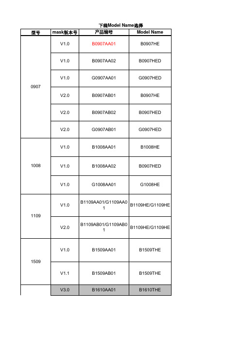
型号mask 版本号产品编号Model Name V1.0B0907AA01B0907HE V1.0B0907AA02B0907HED V1.0G0907AA01G0907HED V2.0B0907AB01B0907HEV2.0B0907AB02B0907HEDV2.0G0907AB01G0907HEDV1.0B1008AA01B1008HEV1.0B1008AA02B0907HEDV1.0G1008AA01G1008HEV1.0B1109AA01/G1109AA01B1109HE/G1109HE V2.0B1109AB01/G1109AB01B1109HE/G1109HEV1.0B1509AA01B1509THE V1.1B1509AB01B1509THEV3.0B1610AA01B1610THE1109下线Model Name 选择100809071509V4.1B1610AB02B1610THE V4.1B1610AB03B1610THE V4.1B1610AB04B1610THE V4.2B1610AC04B1610THE V1.0B2109AA01B2109THE V2.0B2109AB01B2109THEV1.0B2020AA01B2020THMV1.1B2020AA01B2020THMV1.2B2020AB01B2020THM无标注B2410AA01B2410SLV3.0B2410AB02B2410THEV3.0B2410AB03B2410THE210920201610V3.0B2410AB04B2410THE 2410V3.0B2410AB05B2410THEV3.1B2410AC04B2410THEV3.2B2410AD04B2410THEV4.0B2410AE05B2410THEV3.0B2812AA01B2812THEV3.0B2812AA02B2812THEV3.0B2812AA03B2812THEV3.0B2812AA02B2812THE 2812V4.0B2812AB01B2812THEV4.1B2812AC02B2812THERDV1.0B2812AD04B2812THEV5.0B2812AD01B2812THEV2.0B2626AA01B2626THMV2.1B2626AB02B2626THMV2.1B2626AB03B2626THM 2626V2.2B2626AC01B2626THM V2.2G2626AC01G2626THM V1.0B3030AA01B3030THM V1.0B3030AA02B3030THMV2.0B3030AB01B3030THMV2.1B3030AC01B3030THMV2.2B3030AD01B3030THMV1.0B3434AA01B3434THM26263030V1.0B3434AA02B3434THM 3434V2.0B3434AB01B3434THMV2.1B3434AC01B3434THMV1.0B4222AA01B4222THEV2.0B4222AB01B4222THE 4222V2.1B4222AC01B4222THEV1.0B4040AA01B4040THMV1.1B4040AA01B4040THMV2.0B4040AA01B4040THM 4040V2.1B4040AB01B4040THMV1.0B4545AA01B4545THMV1.1B4545AA01B4545THMV2.0B4545AB01B4545THM 4545V2.1B4545AC01B4545THMV1.0B5050AA01B5050THM 5050V2.0B5050AB01B5050THMV1.0B6060AA01B6060THMV2.0B6060AB01B6060THM 6060V2.1B6060AC01B6060THM状态图形备注量产在用普通蓝光非量产在用RGB蓝光非量产在用RGB绿光非量产在用普通蓝光非量产在用RGB蓝光非量产在用RGB绿光非量产在用普通蓝光非量产在用RGB蓝光非量产在用RGB绿光非量产TR在用非量产PIE在用非量产在用非量产在用非量产不在用量产停用Lapping:150um+/-5um量产停用Lapping:130um+/-5um量产在用在ITO和Metal酸洗前增加Wait站别量产在用非量产不在用非量产在用非量产不在用非量产在用非量产在用不在用量产ER、1BH停用Lapping:150um+/-5um量产ER、1BH停用Lapping:130um+/-5um量产ER、1BH在用在ITO和Metal酸洗前增加Wait站别量产Aixron 使用PV recipe改为:PV-test-S200非量产在用非量产在用非量产在用PV:P5000量产ER、1BH停用Lapping:150um+/-5um量产ER、1BH停用Lapping:130um+/-5um量产ER、1BH在用在ITO和Metal酸洗前增加Wait站别非量产在用非量产在用非量产在用非量产在用PV:P5000非量产在用非量产不在用量产停用量产在用在ITO和Metal酸洗前增加Wait站别非量产在用非量产在用绿光量产在用量产在用测试电流由120mA改为350mA 非量产在用非量产在用非量产在用量产停用量产在用在ITO和Metal酸洗前增加Wait站别非量产在用非量产在用非量产不在用非量产在用非量产在用非量产不在用非量产不在用非量产在用非量产在用非量产不在用非量产不在用非量产在用非量产在用非量产不在用非量产在用非量产不在用非量产在用非量产在用。
RT9705B 1 DS9705B-03 电源多路复用器说明书
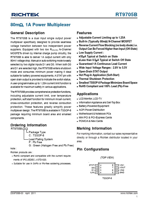
DS9705B-03 April 201180m Ω, 1A Power MultiplexerGeneral DescriptionThe RT9705B is a dual input single output power multiplexer specifically designed to provide seamless voltage transition between two independent power suppliers. Equipped with two low R DS(ON) N-Channel MOSFETs driven by internal charge pump circuitry, the RT9705B is able to deliver 1A output current with only 80mV voltage drop. Manual or auto switching mode is easily selected by two digital inputs D1 and D0. When both D0and D1 are selected high, the RT9705B enters shutdown mode and consumes minimum power making it ideal suitable for battery powered equipments. A STAT pin with open drain output is provided to indicate the switch status.A user-programmable up to 1.25A current limit function is available for maximum safety in various applications.The RT9705B provides comprehensive protection functions,including adjustable current limit, over temperature protection, soft start function for minimum inrush current,cross-conduction protection, and reverse conduction protection. These features greatly simplify power multiplexer design. The RT9705B is available in TSSOP-8package requiring minimum board area and smallest components.Featuresz Adjustable Current Limiting up to 1.25Az Built-In (Typically 80m Ω) N-Channel MOSFET zReverse Current Flow Blocking (no body diode) i.e.Output Can Be Forced Higher than Input (Off-State)zLow Supply Current :`55μA Typical at Switch on State`Less than 0.5μA Typical at Switch Off State z Guaranteed 1A Continuous Load Current z Wide Input Voltage Ranges : 2.8V to 5.5V z Open-Drain STAT Outputz Hot Plug-In Application (Soft-Start)z Thermal Shutdown Protectionz Smallest TSSOP-8 Package Minimizes Board Space zRoHS Compliant and 100% Lead (Pb)-FreeApplicationsz LCD Monitor, LCD-TVz Information Appliance and Set-Top Box z Battery-Powered Equipment z ACPI Power Distributionz Motherboard & Notebook PCs z Mini PCI & PCI-Express Cards zPCMCIA & New CardsPin Configurations(TOP VIEW)TSSOP-8Ordering InformationSTAT D0D1ILIMGNDVIN2VOUT VIN1Note :Richtek products are :` RoHS compliant and compatible with the current require-ments of IPC/JEDEC J-STD-020.` Suitable for use in SnPb or Pb-free soldering processes.Marking InformationFor marking information, contact our sales representative directly or through a Richtek distributor located in yourarea.Package Type C : TSSOP-8RT9705BLead Plating System P : Pb FreeG : Green (Halogen Free and Pb Free)Typical Application CircuitTable 1. Truth TableNotes for Table 1.1. X : Don ’t care2. Hi-Z: High impedance node3. D0 and D1 cannot be floating which will lead to an unknown state.4. An internal MOSFET with 2k Ω R DS(ON) turns on and softly discharges the output voltage when D0 = D1 = 1.V V OUTDS9705B-03 April 2011Test CircuitsTest Circuit 1Test Circuit 2Test Circuit 3Test Circuit 4f = 28Hzf = 580Hz5VV OUTFunction Block DiagramTiming DiagramV 5VQ1 EnabledQ2 EnabledV 3.3VV OUT (a)(b)(c)DS9705B-03 April 2011Electrical Characteristicsz Input Voltage, VIN1 & VIN2-----------------------------------------------------------------------------------------−0.3V to 6.0V z Logic Inputs Voltage, D0 &D1--------------------------------------------------------------------------------------−0.3V to 6.0V z Output Voltage, VOUT , STAT & ILIM -----------------------------------------------------------------------------−0.3V to 6.0V zPower Dissipation, P D @ T A = 25°CTSSOP-8----------------------------------------------------------------------------------------------------------------0.43W zPackage Thermal Resistance (Note 2)TSSOP-8, θJA ----------------------------------------------------------------------------------------------------------230°C/W z Junction T emperature -------------------------------------------------------------------------------------------------125°C z Lead Temperature (Soldering, 10 sec.)---------------------------------------------------------------------------260°Cz Storage T emperature Range ----------------------------------------------------------------------------------------−65°C to 150°C zESD Susceptibility (Note 3)HBM (Human Body Mode)------------------------------------------------------------------------------------------2kV MM (Machine Mode)--------------------------------------------------------------------------------------------------200VAbsolute Maximum Ratings (Note 1)To be continuedRecommended Operating Conditions (Note 4)zInput VoltageV IN1 ( if V IN2 2.8V)--------------------------------------------------------------------------------------------------2.3V to 5.5V V IN1 ( if V IN2 < 2.8V)--------------------------------------------------------------------------------------------------2.8V to 5.5V V IN2 ( if V IN1 2.8V)--------------------------------------------------------------------------------------------------2.3V to 5.5V V IN2 ( if V IN1 < 2.8V)--------------------------------------------------------------------------------------------------2.8V to 5.5V z Logic Inputs Voltage (D0 &D1)-------------------------------------------------------------------------------------0V to 5.5V z Junction T emperature Range ----------------------------------------------------------------------------------------−40°C to 125°C z Ambient T emperature Range ----------------------------------------------------------------------------------------−40°C to 85°C≥≥To be continuedDS9705B-03 April 2011Note 1. Stresses listed as the above “Absolute MaximumRatings ” may cause permanent damage to the device. These are for stress ratings. Functional operation of the device at these or any other conditions beyond those indicated in the operational sections of the specifications is not implied.Exposure to absolute maximum rating conditions for extended periods may remain possibility to affect device reliability.Note 2. θJA is measured in the natural convection atT A = 25°C on a low effective thermal conductivity test board of JEDEC 51-3 thermal measurement standard.Note 3. Devices are ESD sensitive. Handling precautionrecommended.Note 4. The device is not guaranteed to function outside itsoperating conditions.Note 5. Performance at −5°C ≤ T A ≤ 85°C is assured bydesign.Note 6. Not tested for production.Note 7. The UVLO is without latch. In V IN falling dege, theoutput voltage will depend on I OUT and C OUT . Please see below curve as reference.V IN2 = 2.2V, C OUT = 10uF, R L = 180ΩV OUT Response vs. UVLOTime (1ms/Div)V OUT(1V/Div)V IN1(1V/Div)R DS(ON) vs. Temperature5060708090100110-50-25255075100125Temperature (°C)R D S (O N ) (m Ω)Typical Operating CharacteristicsR e f e r t o T e s t C i r c u i t s 2Output Turn-On ResponseTime (1ms/Div)D0D1V OUT(2V/Div)(2V/Div)(2V/Div)D0 = 1 0, D1 = 1, V IN1 = 5V, V IN2 = 3.3V↔Output Switchover ResponseTime (1ms/Div)D1D0V OUT(2V/Div)(2V/Div)(2V/Div)D0 = 0, D1 = 1 0V IN1 = 5V, V IN2 = 3.3V↔R e f e r t o T e s t C i r c u i t s 1Current Limit vs. Junction Temperature00.20.40.60.811.21.41.61.82-50-25255075100125Junction Temperature C u rr e n t L i m i t (A )(°C)R DS(ON) vs. Input Voltage606570758085902.53 3.54 4.55 5.56Input Voltage (V)R D S (O N ) (m Ω)Quiescent Current vs. Input Voltage303540455055602.53 3.54 4.55 5.56Input Voltage (V)Q u i e s c e n t C u r r en t (u A )DS9705B-03 April 2011Output Switchover Voltage DroopTime (50μs/Div)D1V OUT(2V/Div)(2V/Div), C OUT = 1uF (2V/Div), C OUT = openD0 = 0, D1 = 1 0, V IN1 = V IN2 = 5V, RL = 50Ω↔R e f e r t o T e s t C i r c u i t s 3Auto Switchover Voltage DroopTime (250μs/Div)(2V/Div)(2V/Div)V OUTV IN1D0 = 1, D1 = 0, V IN1 = 5 0V, V IN2 = 3.3V↔R e f e r t o T e s t C i r c u i t s 4Output Switchover Voltage Droop vs. C OUT00.20.40.60.811.21.41.60.1110100C OUT (uF)O u t p u t S w i t c h o v e r V o l t a g e D r o o p (V )Application InformationThe RT9705B is dual input single output power multiplexer specifically designed to provide seamless voltage transition between two independent power suppliers. Equipped with two low R DS(ON) N-Channel MOSFETs driven by internal charge pump circuitry, the RT9705B is able to deliver 1A output current with only 80mV voltage drop. The RT9705B provides comprehensive protection functions, including adjustable current limit, over temperature protection, soft start function for minimum inrush current, cross-conduction protection, and reverse conduction protection. These features greatly simplify power multiplexer design.Manual Switching ModeThe RT9705B provides two logic input D0 and D1 for switch selection as shown in Table 1. The RT9705B selects the manual-switching mode when the D0 is pulled low. In this mode V OUT connects to V IN1 if D1 pulled high, otherwise V OUT connects to V IN2.Auto Switching ModeRT9705B selects the auto-switching mode when the D0 is pulled high and D1 is pulled low. In this mode V OUT connects to the higher of V IN1 and V IN2.Shutdown ModeWhen both D0 and D1 are selected high, the RT9705B enters shutdown mode and consumes minimum power. An internal MOSFET with 2kΩ R DS(ON) turns on and softly discharges the output voltage in the shutdown mode. Since no body diode exists between V INX and V OUT, output voltage is allowed to be high than the input voltages in the shutdown mode.Switch Status IndicationA STAT pin with open drain output is provided to indicate the switch status. STAT pin outputs high impedance if V IN2 is active, otherwise STAT pin outputs low.Current LimitingThe current limit circuitry prevents damage to the MOSFET switch and external load. A resistor R ILIM from ILIM to GND sets the current limit to 500/R ILIM and the adjustable current limiting up to 1.25 A. A setting resistor R ILIM equal to zero is not recommended as that disables current limiting.Thermal ConsiderationsThermal protection limits power dissipation in RT9705B. When the operation junction temperature exceeds 135°C, the OTP circuit starts the thermal shutdown function and turns the pass element off. The pass element turn on again after the junction temperature cools by 10°C.For continuous operation, do not exceed absolute maximum operation junction temperature 125°C. The power dissipation definition in device is :P D = (V IN-V OUT) x I OUT + V IN x I QThe maximum power dissipation depends on the thermal resistance of IC package, PCB layout, the rate of surroundings airflow and temperature difference between junction to ambient. The maximum power dissipation can be calculated by following formula :P D(MAX) = ( T J(MAX) - T A ) / θJAwhere T J(MAX) is the maximum operation junction temperature 125°C, T A is the ambient temperature and the θJA is the junction to ambient thermal resistance.For recommended operating conditions specification of RT9705B, where T J(MAX) is the maximum junction temperature of the die (125°C) and T A is the maximum ambient temperature. The junction to ambient thermal resistance (θJA is layout dependent) for TSSOP-8 package is 230°C/W on standard JEDEC 51-3 thermal test board. The maximum power dissipation at T A = 25°C can be calculated by following formula :P D(MAX) = (125°C -25°C) / 230°C/W = 430 mW (TSSOP-8)RT9705B11DS9705B-03 April 2011Layout ConsiderationIn order to meet the voltage drop, droop, and EMI requirements, careful PCB layout is necessary. The following guidelines must be considered :zKeep all main current traces as short and wide as possible.z Place a ground plane under all circuitry to lower both resistance and inductance and improve DC and transient performance (Use a separate ground and power plans if possible).zLocate the ceramic input capacitors as close as possible to the VIN and GND pins of the device.Figure 1. Top Layer Figure 2. Bottom Layer12DS9705B-03 April Richtek Technology CorporationHeadquarter5F, No. 20, Taiyuen Street, Chupei CityHsinchu, Taiwan, R.O.C.Tel: (8863)5526789 Fax: (8863)5526611Richtek Technology Corporation Taipei Office (Marketing)5F, No. 95, Minchiuan Road, Hsintien City Taipei County, Taiwan, R.O.C.Tel: (8862)86672399 Fax: (8862)86672377Email:*********************Information that is provided by Richtek Technology Corporation is believed to be accurate and reliable. Richtek reserves the right to make any change in circuit design,specification or other related things if necessary without notice at any time. No third party intellectual property infringement of the applications should be guaranteed by users when integrating Richtek products into any application. No legal responsibility for any said applications is assumed by Richtek.8-Lead TSSOP Plastic Package。
最新LED恒流驱动芯片汇总
最新LED恒流驱动芯片汇总
LED恒流驱动芯片是一种用于控制LED灯工作电流的电子器件,它可
以帮助提高LED灯的亮度、节能和寿命。
随着LED照明技术的发展,LED
恒流驱动芯片也在不断更新和改进。
以下是一些最新的LED恒流驱动芯片
的汇总介绍。
1.NXPSSL5028GPH:NXPSSL5028GPH是一款数字式LED恒流驱动芯片,集成了多种电流选择和调节功能,可以实现精确的电流控制和亮度调节。
该芯片可广泛应用于室内和室外LED照明产品,具有高效、稳定和可靠的
特点。
2. STMicroelectronics L6924D:STMicroelectronics L6924D是一
款高性能LED驱动芯片,具有高达95%的转换效率。
该芯片采用恒流控制
和PWM调光技术,可以实现高亮度的LED照明效果。
同时,该芯片还具有
热保护和电压保护功能,有效保护LED灯的使用寿命。
4. Infineon ILD8150:Infineon ILD8150是一款集成式恒流驱动芯片,适用于室内和室外LED照明产品。
该芯片采用了新型的TRILINX技术,可以提供高效、低噪声和高稳定性的LED驱动效果。
同时,该芯片还具有
多种保护功能,如过温保护、短路保护和过电流保护等。
以上是一些最新的LED恒流驱动芯片的汇总介绍。
这些芯片具有高效、稳定和可靠的特点,可以实现精确的电流控制和亮度调节,满足不同应用
场景的LED照明需求。
随着LED技术的不断发展,LED恒流驱动芯片将继
续推陈出新,为LED照明市场带来更多创新和发展。
夏普光耦选型手册
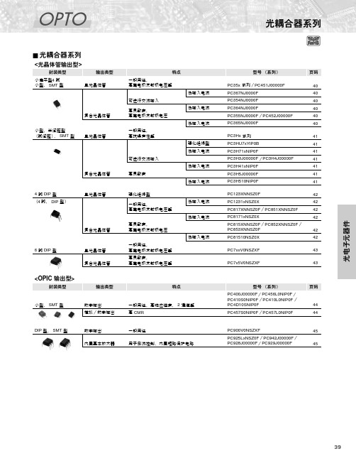
4脚 DIP
PC815XNNSZ0F*5, *6 复 合 光 晶 PC81510NSZ0X 体 管 5, 6 输 PC852XNNSZ0F* * 出 PC853XNNSZ0F*5, *6
*1 *2 *3 *4 *5 *6 *7 *8 *9
–
–
50
5.0
35
600
1
60
100
⅜ ⅜ ⅜
– ⅜ ⅜
–
10
页码 40 40 40 40 40 40 41 41 41 41 41 41 41 42 42 42 42 42 42 43 43
<OPIC 输出型>
封装类型 输出类型 特点 型号 (系列) PC400J00000F/PC456L0NIP0F/ PC410S0NIP0F /PC410L0NIP0F / PC4D10SNIP0F PC457S0NIP0F /PC457L0NIP0F 页码
PC714V0NSZXF PC724V0NSZXF
高绝缘电压 高绝缘电压, 大输入电流 高绝缘电压, 带基底端子 高绝缘电压, 高灵敏度 高绝缘电压, 高灵敏度, 高集电极发射极电压, 大功率
PC3HU7xYIP0B
PC3H2J00000F (小扁平型4脚)
注意: 未经元器件规格说明书确认,便在设备中使用产品目录、数据手册等所刊载的任何夏普元器件,由此引起的故障或损害,夏普公 司将不负任何责任。 除非特别说明,本页所列的型号均符合 RoHS (有害物质限制)标准* 。详情请与夏普公司联系。 *RoHS (有害物质限制)标准:禁止使用铅、镉、六价铬、汞和特定溴系阻燃剂 (PBB 和 PBDE) ,除特别情况外。 因此,在使用任何夏普元器件之前,务请与夏普公司联系以获取最新的元器件规格说明书。
Richtek RT4720AC 三通道DC-DC增压转换器说明书

RT4720ACTriple DC-DC Boost Converter for AMOLEDGeneral DescriptionThe RT4720AC is a triple channels DC-DC converter which is designed to provide the power of AMOLED. It integrates step up DC-DC and an inverting converter to provide the positive and negative output voltage required by AMOLED.For the portable application, board space and efficiency are always major concerns. The high switching frequency of the RT4720AC allows the use of low inductance inductor to save the board space. It provides dual positive output voltage, one is a fixed 5.8V or 7.7V output voltage by SEL pin and the other positive output is fixed 4.6V. For the negative output voltage, it can be programmed by external MCU through single wire (SWIRE pin). The output voltage range of negative output voltage is -1.4V to -5.4V. The RT4720AC has OTP, SCP, UVLO and over-current protections. The RT4720AC is available in a WQFN-16L 3x3 package to achieve saving PCB space.Applications● Cellular Phones ● Digital Cameras● PDAs and Smart Phones ●Probable InstrumentFeatures●Boost Converter to Supply Positive AVDD Voltage Fixed 5.8V or 7.7V●Boost Converter to Supply AMOLED Positive Voltage 4.6V● Inverter Converter to Supply AMOLED Negative Voltage From -1.4V to -5.4V● Maximum Output Current up to 300mA for AMOLED Positive & Negative Power Supply ● Maximum Output Current up to 50mA for Fixed 5.8V or 7.7V AVDD Output Voltage● Typical Peak Efficiency : 90% (40mA to 150mA) ● ********************************● High Output Voltage Accuracy ● Excellent Line and Load Transient ● Excellent Line and Load Regulation● Programmable Negative Voltage by SWIRE Pin ● Fast Outputs Discharge Function● Low Quiescent Current < 1μA in Shutdown Mode ● Internal Soft-Start to limit Inrush Current ● Over-Temperature Protection (OTP) ● Over-Current Protection (OCP) ●Short Circuit Protection (SCP)Simplified Application CircuitVBAT V POSAVDD V NEGRT4720ACOrdering InformationPackage TypeQW : WQFN-16L 3x3 (W-Type)RT4720ACLead Plating SystemG : Green (Halogen Free and Pb Free)Note :Richtek products are :RoHS compliant and compatible with the current requirements of IPC/JEDEC J-STD-020.Suitable for use in SnPb or Pb-free soldering processes.Marking InformationLL= : Product CodeYMDNN : Date CodePin Configuration(TOP VIEW)A V I N P G N D 2L X 3S E L LX1PGND1FBSLX2V O 3PVIN VO2N C E N O 3A G N D VO1SWIRE1211109131415161234876517AGNDWQFN-16L 3x3Functional Pin DescriptionRT4720ACFunctional Block DiagramOperationThe RT4720AC is a triple channels DC-DC converter which is designed to provide the power of AMOLED that can support the input voltage range from 2.9V to 4.5V. The VO1 & VO2 output current can be up to 300mA, and the VO3 output current can be up to 50mA. The RT4720AC uses current mode architecture for the purpose of high efficiency and high transient response. The VO1 positive output voltage is produced from the DC-DC Boost converter and is set at a typical value of 4.6V. When the SWIRE goes high, the positive output voltage will be enabled with an internal soft-start process. The VO2 negative output voltage is produced from the DC-DC buck-boost converter and the negative output voltage range is -1.4V to -5.4V. It can be programmed by external MCU through single wire (SWIRE pin). The VO3 positive output voltage is produced from the DC-DC Boost converter and is set at a fixed 7.7V or 5.8V by SEL pin. When SWIRE goes high and VO1 soft-start had finished already, negative output voltage VO2 will be enabled with an internal soft-start process.RT4720ACTable 1. SWIRE Command LUT for VO2Table 2. SWIRE Pin CharacteristicsRT4720ACTiming DiagramSWIRE Command Timing DiagramSWIREVO1VO20 0Power Sequencet > 300µsVO1 VO20 0RT4720ACAbsolute Maximum Ratings(Note 1)●PVIN, AVIN, VO1, LX1, FBS, SEL, ENO3, SWIRE ----------------------------------------------------------- -0.3 to 6V●VO3, LX3 ---------------------------------------------------------------------------------------------------------------- -0.3 to 12V●VO2 ----------------------------------------------------------------------------------------------------------------------- -6 to 0.3V●LX2 ------------------------------------------------------------------------------------------------------------------------ -6 to 6V●Power Dissipation, P D @ T A = 25︒CWQFN-16L 3x3 -------------------------------------------------------------------------------------------------------- 3.33W●Package Thermal Resistance (Note 2)WQFN-16L 3x3, θJA -------------------------------------------------------------------------------------------------- 30︒C/WWQFN-16L 3x3, θJC -------------------------------------------------------------------------------------------------- 7.5︒C/W●Lead Temperature (Soldering, 10sec.) --------------------------------------------------------------------------- 260︒C●Junction Temperature ------------------------------------------------------------------------------------------------ 150︒C●Storage Temperature Range --------------------------------------------------------------------------------------- -65︒C to 150︒C ●ESD Susceptibility (Note 3)HBM (Human Body Model) ----------------------------------------------------------------------------------------- 2kV Recommended Operating Conditions (Note 4)●Supply Input Voltage ------------------------------------------------------------------------------------------------- 2.9V to 4.5V●Ambient Temperature Range -------------------------------------------------------------------------------------- -40︒C to 85︒C ●Junction Temperature Range -------------------------------------------------------------------------------------- -40︒C to 125︒C Electrical Characteristics(V IN = 3.7V, V O1 = 4.6V, V O2 = -4V, V O3 = 7.7V, T A = 25︒C, unless otherwise specified)RT4720ACRT4720ACNote 1. Stresses beyond those listed “Absolute Maximum Ratings” may cause permanent damage to the device. These are stress ratings only, and functional operation of the device at these or any other conditions beyond those indicated in the operational sections of the specifications is not implied. Exposure to absolute maximum rating conditions may affect device reliability.Note 2. θJA is measured under natural convection (still air) at T A= 25°C with the component mounted on a high effective-thermal-conductivity four-layer test board on a JEDEC 51-7 thermal measurement standard. θJC is measured at the exposed pad of the package.Note 3. Devices are ESD sensitive. Handling precaution recommended.Note 4. The device is not guaranteed to function outside its operating conditions.RT4720ACTypical Application CircuitVBAT V POS(Fixed 4.6V)AVDD (5.8V & 7.7V)V NEGTable 3. Typical BOM ListRT4720ACTypical Operating CharacteristicsVO1 & VO2 Efficiency vs. Load Current707580859095100E f f i c i e n c y (%)VO3 Efficiency vs. Load Current707580859095100E f f i c i e n c y (%)VO3 Efficiency vs. Load Current707580859095100E f f i c i e n c y (%)4.564.574.584.594.604.614.624.634.6450100150200250300Load Current (mA)V O 1 V o l t a g e (V )-4.04-4.03-4.02-4.01-4.00-3.99-3.98-3.97-3.96050100150200250300Load Current (mA)V O 2 V o l t a g e (V )VO3 Voltage vs. Load Current7.647.667.687.707.727.741020304050Load Current (mA)V O 3 V o l t a g e (V )VO3 Voltage vs. Load Current5.745.755.765.775.785.795.805.815.825.835.8401020304050Load Current (mA)V O 3 V o l t a g e (V )V IN = 3.7VCTRL (5V/Div)VO1(2V/Div)VO2(2V/Div)I IN(500mA/Div)Time (2ms/Div)VO1 & VO2 Power OnCTRL (5V/Div)VO1(2V/Div)VO2(2V/Div)I IN(500mA/Div)Time (2ms/Div)VO1 & VO2 Power OffV IN = 3.7VEN_VO3(5V/Div)VO3(2V/Div)Time (2ms/Div)VO3 Power On (SEL = L)V IN = 3.7VI IN(500mA/Div)EN_VO3(5V/Div)VO3(2V/Div)Time (2ms/Div)VO3 Power Off (SEL = L)V IN = 3.7VI IN(500mA/Div)Application InformationThe RT4720AC is a triple channels DC-DC converter, which integrates dual step up converter and an inverting converter to provide the positive and negative output voltage required by AMOLED. The RT4720AC protection function includes Over-Temperature Protection (OTP), Over-Current Protection (OCP) and Short Circuit Protection (SCP), also it has Pulse Skipping Mode (PSM) to provide high efficiency during light load.Soft-StartThe RT4720AC use an internal soft-start feature to avoid high inrush currents during step-up.Fast Discharge FunctionAll outputs voltage use an embedded discharge function to discharge the remaining output to 0V rapidly, preventing phenomena such as residual image on the display during shutdown.Over-Temperature Protection (OTP)The RT4720AC includes an Over-Temperature Protection (OTP) feature to prevent excessive power dissipation from overheating the device. The OTP will shut down switching operation when junction temperature exceeds 140︒C. Once the junction temperature cools down by approximately 15︒C, the converter resumes operation.To maintain continuous operation, prevent the maximum junction temperature from rising above 125︒C.Over-Current Protection (OCP)The RT4720AC includes a current sensing circuitry which monitors the inductor current during each ON period. If the current value becomes greater than the current limit, the switch that pertains to inductor charging will turn off, forcing the inductor to leave charging stage and enter discharge stage.Short Circuit Protection (SCP)The RT4720AC has an advanced short circuit protection mechanism which prevents damage to the device from unexpected applications. When the output voltage becomes lower than about 90%, over 1ms the device enters shutdown mode. VO3 can only re-start normal operation after triggering the ENO3 pin and VO1, VO2 can only re-start normal operation after triggering the SWIRE pin.Under-Voltage Lockout (UVLO)To prevent abnormal operation of the IC in low voltage condition, an under-voltage lockout is included, which shuts down the device at voltages lower than 2.2V. All functions will be turned off in this state.Input Capacitor SelectionEach channel input ceramic capacitors with 10μF capacitance are suggested for the RT4720AC applications. However, to achieve best performance with the RT4720AC, larger capacitance can be used. For better voltage filtering, select ceramic capacitors with low ESR, X5R and X7R types which are suitable because of their wider voltage and temperature ranges.Boost Inductor SelectionThe inductance depends on the maximum input current. As a general rule, the inductor ripple current range is 20% to 40% of the maximum input current. If 40% is selected as an example, the inductor ripple current can be calculated according to the following equations :OUT OUT(MAX)IN(MAX)INL IN(MAX)V II=ηVΔI= 0.4I⨯⨯⨯where η is the efficiency of the converter, I IN(MAX) is the maximum input current, and ΔI L is the inductor ripple current. The input peak current can then be obtained by adding the maximum input current with half of the inductor ripple current as shown in the following equation :I PEAK = 1.2 × I IN(MAX)Note that the saturated current of the inductor must be greater than I PEAK.The inductance can eventually be determined according to the following equation :()()()2IN OUT IN2OUT OUT(MAX)OSCηV V-VL =0.4V I f⨯⨯⨯⨯⨯where f OSC is the switching frequency. For better system performance, a shielded inductor is preferred to avoid EMI problems.Boost Output Capacitor SelectionThe output ripple voltage is an important index for estimating chip performance. This portion consists of two parts. One is the product of the inductor peak current with the ESR of the output capacitor, while the other part is formed by the charging and discharging process of the output capacitor. As shown in Figure 1, ΔV OUT1 can be evaluated based on the ideal energy equalization. According to the definition of Q, the Q value can be calculated as the following equation :IN L OUT IN L OUT IN OUT OUT1OUT OSC111Q = I +ΔI -I +I -ΔI -I 222V 1= C V V f ⎡⎤⎛⎫⎛⎫⨯ ⎪ ⎪⎢⎥⎝⎭⎝⎭⎣⎦⨯⨯⨯where f OSC is the switching frequency and ΔI L is the inductor ripple current. Bring C OUT to the left side to estimate the value of ΔV OUT1 according to the following equation :OUTOUT1ESR OUT OSCD I ΔV = ΔV +ηC f ⨯⨯⨯where ESR C C_ESR PEAK C_ESR ΔV = ΔI R = I R ⨯⨯ The output capacitor, C OUT , should be selected accordingly.Figure 1. The Output Ripple Voltage without theContribution of ESRAVDD Output Voltage SettingThe AVDD boost output voltage VO3 is fixed 7.7V or 5.8V output voltage by SEL pin. When SEL pin is set to high, the output voltage is 5.8V or otherwise SEL pin is set to low, the output voltage is changed to 7.7V. Buck-boost Converter Inductor SelectionThe first step in the design procedure is to verify whether the maximum possible output current of the buck-boost converter supports the specific application requirements. To simply the calculation, the fastest approach is to estimate converter efficiency by taking the efficiency numbers from provided efficiency curves or to use a worst case assumption for the expected efficiency, e.g., 80%. The calculation must be performed for the minimum assumed input voltage where the peak switch current is the highest. The inductor has an internal switch to be able to handle this current.④Converter Duty Cycle :OUT IN OUT-V D =V η-V ⨯④Maximum output current :()IN OUT PEAK OSC V D I = I -1-D 2f L ⎛⎫⨯⨯ ⎪⨯⨯⎝⎭④Inductor peak current :OUT IN PEAK OSC I V D I =+1-D 2f L⨯⨯⨯ As for inductance, we are going to derive the transition point, where the converter toggles from CCM to DCM. We need to define the point at which the inductor current ripple touches zero, and as the power switch SW is immediately reactivated, the current ramps up again. Figure 2 portrays the input current activity of the buck-boost converter.Figure 2. The Buck-Boost Input Signature in BCM The inductance can eventually be determined according to the following equation :2OUT IN critical OSC OUT IN OUTV ηV L =2f I V +V ⎛⎫⨯⨯⎪ ⎪⨯⨯⎝⎭Buck-Boost Converter Output Capacitor Selection For the best output voltage filtering, low ESR ceramic capacitors are recommended. One 22μF output capacitors with sufficient voltage ratings in parallel are adequate for most applications. Additional capacitors can be added to improve load transient response. To calculate the output voltage ripple, the following equations can be used :OUTESR OSC LOAD OUTD V ΔV =+ ΔV f R C ⨯⨯⨯where ESR C C_ESR PEAK C_ESRΔV = ΔI R = I R ⨯⨯∆V ESR can be neglected in many cases since ceramic capacitors provides very low ESR. Negative Output Voltage SettingBuck-boost converter is implementing a pulse dimming method to control the output voltage (VO2) and its value is from -1.4V to -5.4V in 0.1V increments. User can control VO2 by SWIRE command. See SWIRE command section for details on how to adjust the output voltage.Thermal ConsiderationsThe junction temperature should never exceed the absolute maximum junction temperature T J(MAX), listed under Absolute Maximum Ratings, to avoid permanent damage to the device. The maximum allowable power dissipation depends on the thermal resistance of the IC package, the PCB layout, the rate of surrounding airflow, and the difference between the junction and ambient temperatures.Themaximumpowerdissipation can be calculated using the followingformula :P D(MAX) = (T J(MAX) - T A ) / θJAwhere T J(MAX) is the maximum junction temperature,T A is the ambient temperature, and θJA is the junction-to-ambient thermal resistance.For continuous operation, the maximum operating junction temperature indicated under Recommended OperatingConditionsis125°C.Thejunction-to-ambient thermal resistance, θJA , is highly package dependent. For a WQFN-16L 3x3 package, the thermal resistance, θJA , is 30°C/W on a standard JEDEC51-7higheffective-thermal-conductivityfour-layer test board. The maximum power dissipation at T A = 25°C can be calculated as below :P D(MAX) = (125°C - 25°C) / (30°C/W) = 3.33W for a WQFN-16L 3x3 package.The maximum power dissipation depends on the operating ambient temperature for the fixed T J(MAX) and the thermal resistance, θJA . The derating curves in Figure 3 allows the designer to see the effect of rising ambient temperature on the maximum power dissipation.Figure 3. Derating Curve of Maximum PowerDissipationLayout ConsiderationsFor the best performance of the RT4720AC, the following PCB layout guidelines should be strictly followed.For good regulation, place the power components asclose to the IC as possible. The traces should be wide and short, especially for the high current output loop.0.00.51.01.52.02.53.03.5255075100125Ambient Temperature (°C)M a x i m u m P o w e r D i s s i p a t i o n (W )④The input and output bypass capacitor should be placed as close to the IC as possible and connected to the ground plane of the PCB.④Minimize the size of the LX1, LX2, LX3 nodes and keep the traces wide and short. Care should be taken to avoid running traces that carry any noise-sensitive signals near LX or high-current traces. ④Separate power ground (PGND) and analog ground (AGND). Connect the AGND and the PGND islands at a single end. Make sure that there are no other connections between these separate ground planes.④Connect the exposed pad to a strong ground plane for maximum thermal dissipation.Figure 4. PCB Layout GuideOutline DimensionW-Type 16L QFN 3x3 PackageFootprint InformationRichtek Technology Corporation14F, No. 8, Tai Yuen 1st Street, Chupei CityHsinchu, Taiwan, R.O.C.Tel: (8863)5526789Richtek products are sold by description only. Richtek reserves the right to change the circuitry and/or specifications without notice at any time. Customers should obtain the latest relevant information and data sheets before placing orders and should verify that such information is current and complete. Richtek cannot assume responsibility for use of any circuitry other than circuitry entirely embodied in a Richtek product. Information furnished by Richtek is believed to be accurate and reliable. However, no responsibility is assumed by Richtek or its subsidiaries for its use; nor for any infringements of patents or other rights of third parties which may result from its use. No license is granted by implication or otherwise under any patent or patent rights of Richtek or its subsidiaries.。
各大LED驱动芯片大全

不知道发过没?各大LED驱动芯片大全Fairchild (美国飞兆) FSEZ 1016主要应用于3W灯杯3WFSEZ 1216主要应用于5W灯杯5WFSQ 110主要应用于8W左右LED电源8WFSDH 321主要应用于8W左右LED电源8WKA5M02659RN主要应用于12W左右LED电源12WKA5M0365R/KA5M0380RYDTU主要应用于30W左右LED电源30WFSDL0165/FSDM0265/FSDM0365 主要应用于12-18WLED电源12-18WKA5L0365RN/KA5M0365RN主要应用于24WLED电源25WSG6859 + 2N60/4N60主要应用于日光灯等外置式LED电源30W 以下SG6741 + 7N60C/7N60C主要应用于日光灯等外置式LED电源60W 以下FSFR2100主要应用于LED路灯和大功率LED电源200W待补充Power Integrations (PI) LNK603/613PG/DG主要应用于2.5W的LED灯杯2.5WLNK604/614PG/DG主要应用于3.5W的LED灯杯3.5WLNK605/615PG/DG主要应用于4.5W的LED灯杯4.5WLNK606/616PG/GG主要应用于5.5W的LED灯杯5.5WTNY274/275/276/277P/G主要应用于5-8W LED电源5-8WTNY278/279/280P/G主要应用于10-14W LED电源10-14W待补充Supertex (美国超科) AT9933专为汽车设计用高达70V功率驱动ICHV9921/22/2385 to 264V AC or DC input voltage of 20 to400V. 20/30/50mAHV9925Output Current to 50mA;Universal 85-264V AC Operation;Fixed OFF-Time BuckConverter;Internal 500V Power MOSFETHV9903Power efficiency of up to 85%;Drives up to 6 White LEDs;2.6V to 4.6VSupply;power stage can operate at 1.8V;Built-in Soft Start;DC and PWM DimmingControlHV9910高压大功率直驱LED恒流器件HV9911高压双向检测大功率直驱LED恒流ICHV9931高压双向检测大功率直驱LED恒流IC,可PWM灰度调节待补充National (美国国半) 针对带有双电流槽和与IC兼容亮度控制的白色LED和QLED显示器的高效升压器LM3402针对高功率LED驱动器、6V至42V输入电压范围的0.5A持续电流降压电路LM3402HV 针对高功率LED驱动器,6V至75V输入电压范围的0.5A持续电流降压电路LM3404针对高功率LED驱动器,6V至42V输入电压范围的1A持续电流降压电路LM3404HV 针对高功率LED驱动器、6V至75V输入电压范围的1.0A持续电流降压电路LM5022针对升压和SEPIC稳压器的60V低压侧控制器,允许控制外部MOSFET来为LED提供LM2735 520kHz/1.6MHz - 有效使用空间的升压和SEPIC DC-DC稳压器LM3405用于LED驱动器500kHz/1.6MHz 1A恒流降压稳压器LM2754具有超时保护功能的800mA开关电容Flash LED驱动器LM27965具有I2C兼容亮度控制功能的双显示器白光LED驱动器LM27966带有I2C兼容接口的白光LED驱动器LM2727/ LM2737 频道的FET 同步的为低输出电压顽强反抗调整者控制器待补充美国国家半导体公司白色LED低功率驱动部分LM3519高的频率推进白色LED用高速的PWM 光亮控制驱动ICLM2731SOT23 小封装小功率LED驱动应用SOT23 小封装5V升压到12-30V,120-300mALM26238-14V 转换成输出电压在1.24-14V之间,达到90% 的效率LM3557为白色LED2.7V-7.5V的递升转换器,多大5颗LED小体积背光指示LM35022.5-5.5V升压到16-44V,多达4-10颗LED小体积背光指示LM27512 X,1.5 X 电容器式倍压白色LED的引导驱动ICLM3590系列小功率白色LED简单驱动,降压型LM2707系列小功率白色LED简单驱动,升压型LM35082.7Vto5.5V 升压17.5V 驱动4个白色LED达到30mA 应用ICLM2793白色的低噪音引2.5-5.5V,1.5倍压双重的功能光亮控制ICLM2792接受输入电压从3.0V到5.8V的范围和维持持续的电容器类光亮控制LM2791受输入电压从3V到5.8V的范围和维持持续的36mA由外部的固定电阻决定. LM2705直流的升压式150mA的直流转换器LM2703直流的升压式350mA的直流转换器LM3501同时的递升直流/ 直流转换器为白色LED的驱动LM2794/LM2795 多路驱动补给的电容器类比和PWM 灰度控制LM27953 白色LED四路的和3/2 x转变了电容器推进式驱动LM3570低的噪音白色LED,应用与手持式设备多路控制多颗LED背光指示LM3595 平行的白色LED驱动应用LM2704 2.2-7V升压20V,550mA,SOT小封装LED驱动LM2750 低的噪音转变了电容器小功率升压驱动LM2796 双重的3/2 x 的白色LED驱动电容器式应用ICLM27964 有I2C 的独立控制的,多按键区域背光指示应用ICLM2756有I2C 的独立控制的,多按键区域背光指示应用ICLM2754带有超时保护功能的800mA开关电容器Flash LED驱动器LM3551/LM35521A白色用闪光灯驱动应用LM3224直流的递升PWM 的615 KHz/1.25 MHz/直流转换器待补充美国国家半导体公司照明管理单元(LMU)LM4970声音同步化LED驱动器IC适合任何颜色LP3943RGB/白色/ 蓝色16通道引导的LED驱动器LP3944RGB/白色/ 蓝色8 通道引导的LEDLP5520RGB背光LED驱动器LP5521可编程的三通道LED 驱动器LP5522可编程的LED驱动器LP3958高电压推进的照明管理转换器LED应用ICLP5526高的电压推进的照明管理可达到150mA序列闪光的驱动ICLP3936为六白色的照明管理系统引导和一RGB 或闪光引导LP3931双路的RGB 用高亮度驱动DC-DC转换器LP3933为六白色的照明管理系统应用和二RGB 或闪光应用ICLP3954电话LED指示包括展览背光、RGB、按键区和照相机闪光等应用LP3950颜色用声音的同步装置引导LED驱动LP39526个通道的颜色用声音的同步引导驱动应用ICLP39542多路LED背光管理ICLP55281四路RGB驱动器LP5527为照相机闪光的极小驱动和4以I2C应用Programmability,连接性测试和声音LP55271为照相机闪光的极小驱动和4以I2C应用Programmability,连接性测试和声音待补充International Rectifier (IR) IRS2540S/2540PBF一款高压,高频降压调节控制集成电路,该产品用于要求多个LED的交流-直流离线,非隔离应用电路或要求直流-直流混合色能力的应用.应用包括室内外标牌,以及建筑,娱乐,设计和装饰照明.IRS2541S/2541PBF一款高压,高频降压调节控制集成电路,该产品用于要求多个LED的交流-直流离线,非隔离应用电路或要求直流-直流混合色能力的应用.应用包括室内外标牌,以及建筑,娱乐,设计和装饰照明.待补充Nxp (恩智浦) LED屏幕配套部分逻辑IC,飞利浦系列:74HC595D逻辑8位移位寄存器74HC245D3态8总线收发器74HC138D3-8线译码器、多路转换74HC164D8位移位寄存器(串进并出)74HC04D逻辑6非门74HC08D逻辑6非门驱动器74HC244D8缓冲/线驱动/线接收(3态)待补充Maxim-Dallas (美国美信) 美国美信高亮度LED驱动器部分MAX16800高电压6.5-40V驱动35-350mA多颗LED应用驱动ICMAX16801A/BPWM 控制器265V AC-85V AC1A LED驱动器MAX16802A/BPWM 控制器10.8VDC-24VDC 1A LED驱动器MAX16803 高压、350mA、高亮度LED驱动器, 提供PWM亮度调节和5V稳压器MAX16804 高电压5.5V-40V,350mA驱动和PWM 控制暗淡MAX16805/MAX16806 EEPROM可设计的,高电压,350mA台灯等现场调光驱动应用MAX16807/MAX16808 集成8通道LED驱动器,具有开关模式boost及SEPIC控制器MAX16809/MAX16810 集成16通道LED驱动器,具有开关模式boost及SEPIC控制器MAX168181.5 MHz,30A高效率LED恒流驱动MAX16819/MAX168202MHz高光亮LED驱动和5000:1灰度等级调节MAX16823高电压4.5-40V,3通道独立,5mA到70mA和外接BJT时可达到2AMAX16824/MAX16825 3通道、高亮度LED (HB LED)驱动器,6.5V至28V输入电压MAX7302低电压LED驱动器,提供闪烁控制、PWM调节、瞬变检测及电平转换待补充美国美信白光LED驱动器部分MAX8678白光LED在喇叭上整合应用ICMAX1698,MAX1698A便携式LCD屏背光源白光LED驱动应用ICMAX1848手机等小屏锂电池单色LED背光源恒流驱动ICMAX1916小体低压差式恒流驱动ICMAX1910/MAX1912锂电池1.5x/2x倍压式LED驱动器,最大120mAMAX1570锂电池1x/1.5x 倍压式LED驱动器,多路可PWM调光MAX1984/MAX1985/MAX1986白色LED超高效率恒流驱动MAX1582/MAX1582Y可编程升压型2段恒流驱动ICMAX1553/MAX1554高效率, 升压到40V为2 到10 白色LED的转换器驱动MAX1573白色泵式1 x/1.5 x驱动器,小体积QFN型封装MAX1561/MAX1599高效率,升压型转换器26V驱动2到6颗白色LED驱动MAX1574180mA,1x/2x倍压白色泵式驱动IC 3毫米x3毫米TDFN小封装MAX1583白色的引导照相机-闪光推进转换器MAX1575白色LED驱动1x/1.5x电荷泵式光源指示MAX1576480mA白色LED1x/1.5x/2x电荷泵式从背光照亮到照相机闪光灯应用MAX1578/MAX1579TFT屏与LED背光整合驱动应用ICMAX8595Z/MAX8596Z高效率,2.6-5.5V升压型32V,25mA,2-8颗LED驱动应用MAX1577Y/MAX1577Z1.2 A 白色LED闪光灯应用ICMAX8630W/MAX8630X125mA 1x/1.5x电荷泵式为5颗白色LED小型TDFN封装MAX8631X/YLED电荷泵式1x/1.5x/2x4毫米x 4毫米的二LDOs使QFN超薄封装MAX8790六线白色LED恒流驱动,适合笔记本等中尺寸LCD背光MAX8607为1.5A的1MHz PWM 推进转换器白色LED应用照相机闪光MAX8647/MAX8648 超高效率电荷泵式6LED的/ RGB驱动应用,瘦小的QFN封装待补充ONSEMI (美**森美) NCP56122通道泵式可PWM的白色LED驱动产品是LCD屏背光照明,操作模态1 x 和1.5 x 泵式驱动,87% 效率连同0.2% 相配误差.NCP5623带I2C控制的三路输出RGB LED驱动器,完全支持RGB照明或白光LED背光,内置”渐进调光”功能,能效高达94%的电荷泵,具备1x和2x两种工作模式,采用节省空间的极小型LLGA-12 2.0×2.0×0.5 mm封装NCP3065, NCV3065输出1.5 A ,输入电压 3.0 V to 40 V, PWM灰度调节,为汽车应用设计NCP5007小型小体2.7 to5.5 V 升压驱动多颗LED,小屏背光及背光指示等应用NCP5008,NCP50092.7 到6.0 V 输入电压范围,从Vbat 到15 V 的输出电压,外设光敏电阻NCP5010: Integrated Backlight LED BoostDriverNCP5030: Buck-Boost Converter to Drive aSingle LED from 1 Li-Ion or 3 Alkaline BatteriesNCP5604A, NCP5604BHigh Efficiency White LEDDriverNCP5603: High Efficiency Charge PumpConverter / White LED DriverNCP5602: 2-Channel Charge Pump White LEDDriver with I²C ControlNUD4001AC−DC 输入5.0 V, 12 V or 24 V.输出最大500mA,最简易型LED驱动ICNUD4011AC−DC 输入最大120 V.输出最大70mA,最简易型多颗LED驱动ICZetex (英国ZETEX ) ZXLB1600 LED/OLED 升压偏置1.6 - 5.5 28 75 350 MSOP10ZXLD1100 LED 升压驱动器2.5 - 5.5 28V(最大) 60 350 SC70-6ZXLD1101 LED 升压驱动器2.5 - 5.5 28V(最大) 60 350 TSOT23-5ZXLD1320 内置开关式1.5A LED 驱动器4 至18 18 122000 TDFN1433 ZXLD1321 内置开关式1A LED 驱动器1.2 至12 18 122000 TDFN1433 ZXLD1322 内置开关式0.7A LED 驱动器2.5 至15 18 122000 DFN1433 ZXLD1350 内置开关式350mA LED 驱动器7 至30 30 15 370TSOT23-5 ZXLD1360 内置开关式1A LED 驱动器7 至30 30 201000 TSOT23-5 ZXLD1362 内置开关式1A LED 驱动器6 至60 60 651000 TSOT23-5 ZXLD1575 x1/x1.5 充电泵6 通道驱动器2.7 至5.5 5.5 1000120 QFN1644 ZXLD1601 LCD/OLED 升压偏置2.5 - 5.5 VIN 至28 60 320 SC70-6ZXLD1615 LCD/OLED 升压偏置2.5 - 5.5 VIN 至28 60 320 TSOT23-5 ZXLD1937 LED 升压驱动器2.5 - 5.5 28V(最大) 60 350 TSOT23-5ZXSC300 LED 升压/降压驱动器0.8 -8.0 Vin 至Vm 200 外置开关SOT23-5 ZXSC310 LED 升压/降压驱动器0.8 -8.0 Vin 至Vm 200 外置开关SOT23-5 ZXSC380 内置开关式单室简易升压0.8 - 6.0 Vin 至20V 80 - SOT23ZXSC400 LED 升压驱动器1.8 - 8.0 Vin 至Vm 150 外置开关SOT23-6 ZXSC440 相机闪光灯驱动器1.8 - 8.0 Vin 至Vm 150 外置开关MSOP8待补充Texas Instruments (TI) TI 美国德州仪器公司屏幕驱动部分TLC59048/16 通道LED 驱动器TLC59058/16 通道LED 驱动器TLC591116 通道LED 驱动器TLC5916/TLC59178通道LED驱动器TLC592016 通道LED 驱动器TLC592116 通道LED 驱动器TLC5922带有点校正的16 通道LED 驱动器TLC5923带有点校正的16 通道LED 驱动器TLC5924具有点校正功能和预充电FET 的16 通道LED 驱动器TLC593012 通道LED 驱动器TLC5940带有EEprom 点校正与灰度PWM 控制的16 通道LED 驱动器TLC5941带有点校正与灰度PWM 控制的16 通道LED 驱动器TLC5945带有点校正、灰度PWM 控制和无延迟的16 通道LED 驱动器TI 美国德州仪器公司白光LED驱动器TPS60250具有I2C 接口的用于7 个WLED 的1.2A 高功率高效充电泵TPS60251具有I2C 接口的用于7 个WLED 的1.2A 高功率高效充电泵TPS60252同步推进转换器I2C/可并立的接口白色驱动器TPS6102*可调节、1.5A 开关、96% 高效升压转换器,具有降压模式TPS61040/41用于LCD 和白光LED 的,输入1.8-6V出28V 400mA 开关升压转换器TPS61042输入1.8-6V出30V 500mA 开关升压转换器,用于白光LED 应用领域TPS61043升压PWM灰度可调恒流LED驱动TPS6104528V 85% 效率的升压转换器,用于LCD 应用领域TPS61055具有I2C 兼容接口的 1.2A 高功率白光LED 驱动器TPS61058具有1.1A 开关的高功率单个白光LED 驱动器TPS61059具有1.5A 开关的高功率单个白光LED 驱动器TPS61060/TPS61061/TPS61062具有白光LED 亮度控制电源的15V、400mA 开关,1MHz 升压转换器TPS61080具有集成功率二极管的27V、500mA 开关、1.2MHz 升压转换器TPS61081具有集成功率二极管的27V、500mA 开关、1.2MHz 升压转换器TPS61140具有OLED和LCD背光屏双重驱动的应用ICTPS61141具有OLED和LCD背光屏双重驱动的应用ICTPS61150使用单一控制双输出LED驱动背光源驱动ICTPS61151使用单一控制双输出LED驱动背光源驱动ICTPS61150A使用单一控制双输出背光源驱动多大14颗LED能力的ICTPS61160PWM白光LED 2.7-18V升压500mA,最多6pcs LEDTPS61161PWM白光LED 2.7-18V升压500mA,最多10pcs LEDTPS61165PWM白光LED 3-18V升压1.2A,最多3pcs LEDTPS75103LDO低压差背光源LED驱动ICTPS75105LDO低压差背光源LED驱动ICTPS61180/1/25-24V输入多路25mA,最大10WLED背光驱动ICToshiba (日本东芝) TB627258位移位恒流驱动ICTB62726AN/AF16位全彩LED大屏幕TB62726ANG/AFG16位全彩LED大屏幕TCA62746AFG/AFNG16位全彩LED大屏幕带断、短路侦测及温度保护Siti (台湾点晶科技股份) DD311单信道大功率恒流驱动IC最大1A最高耐压36V线性恒流ICDD312单信道大功率恒流驱动IC最大1A最高耐压18V线性恒流ICDD313三信道大功率恒流驱动IC500mA R/G/B恒流驱动ICDM412三通道装饰照明专用可直接数据级联恒流IC 200mA R/G/B恒流驱动ICDM413三通道装饰照明专用PWM输出驱动IC 100mA R/G/B恒流驱动ICDM114,DM115新版8位驱动IC 主要是用于屏幕及灯饰DM115B通用8位恒流驱动IC 恒流一致性及稳定性高DM11A8位恒流动,用于护栏管,屏幕灯饰使用DM11C8位驱动IC 具有短断点侦测及温度保护功能,屏幕灯饰使用DM13C16位驱动IC 具有短断点侦测及温度保护功能,屏幕灯饰使用DM13A16位恒流驱动,面对低端屏幕客户DM134,DM135, DM13616位驱动IC 主要用于LED屏幕及护栏管DM13216位1024级PWM输出驱动ICDM13716位开,短路,过温智能侦测驱动ICDM13316位开路检测&64级电流调整&过温警示驱动ICDM1638x3信道4096级PWM驱动ICDM6214×3装饰照明专用PWM输出驱动恒流ICDM63112比特内置PWM+实时检测恒流驱动ICDM63216比特内置PWM+实时检测恒流驱动ICDM1638×3通道4096级PWM输出恒流驱动ICDM1648×3通道4096级PWM输出恒流驱动ICDD211二倍升压驱动IC 2-3.3V 最大升压100mA固定式恒流ICDD2313信道驱动IC 5-30mA 可设置小体上电即亮型ICDD2334信道驱动IC 5-30mA 可设置小体、可开关型ICDD2121.5-5.5V二倍升压最大400mA电流输出驱动单颗LED恒流ICPC112,PC1132.8-5V四倍升压驱动20mA小功率多颗LED恒流ICST2225A35输出信道之数字/字母LED驱动芯片Addtek (广鹏科技)A701、A702固定式5-30mA灯饰恒流A703120mA可开式6-50V降压型恒流ICA705220mA、2.7-12V固定降压型单路恒流ICA7065-40mA、5-50V/PWM多路可开关型恒流ICAMC711x固定式小电流灯饰应用AMC711x_E固定式小电流灯饰应用AMC71352-6V低压差固定式恒流驱动IC1颗LEDAMC71405-50V DC&DC 最大500mA电流可调,1颗或多颗LED驱动ICAMC71505-24V DC&DC 最大1.5A固定式,1-3颗LED驱动ICAMC7169LED保护ICMBI (台湾聚积科技) MBI18011路恒流驱动1.2A电流可设定PWM信号灰度调节MBI18022路恒流驱动360mA电流可两路单独设定PWM信号灰度调节MBI18044路恒流驱动240mA电流可设定PWM信号灰度调节MBI181616路恒流驱动电流可设定PWM信号灰度调节MBI5024面对低端客户16位LED屏幕、护栏灯管恒流驱动ICMBI502516位最大45mALED屏幕、护栏灯管恒流驱动ICMBI502616位最大90mA LED屏幕、护栏灯管恒流驱动ICMBI502816位最大90mA LED屏幕、护栏灯管恒流驱动IC,具电流增益功能MBI503016位内置PWM高灰阶LED恒流驱动ICMBI503116位内置PWM高灰阶LED恒流驱动IC,相对5030低端客户MBI5039MBI51688位LED屏幕、护栏灯管恒流驱动ICMBI60103位级联式LED灯饰屏幕,R/G/B单独电流可设置恒流驱动IC StarChips (晶錡科技) SCT202416位移位LED恒流驱动,适合目前LED大屏幕使用3-40mASCT202616位移位LED恒流驱动,适合目前LED大屏幕使用3-90mASCT221016位移位LED恒流驱动,适合LED大屏幕及插件护栏管使用3-120mASCT21108位移位LED恒流驱动IC,主要用于灯饰产品SCT251212位移位护栏管专用IC,3路OE灰度可以单独调节SCT20073路点光源驱动IC,可兼容MIB6010Shamrock (台湾芯瑞)SMD7333-40V电压输入,内置MOS管降压型驱动电流1ASMD7353-40V电压输入,降压型驱动电流700mA(可替代AMC7150)SMD736最高40V电压输入,内置MOS管降压型驱动电流3ASMD802市电直驱1A LED驱动IC(可替代HV9910)SMD911市电直驱IC,外置MOS LED隔离方案驱动ICSMD912市电隔离型直驱IC,外置MOS LED驱动ICOB (台湾昂宝) OB656380W PFC Module 400V 0.2ATM PFCOB6573300W PFC Module 400V 0.75A CCM PFCOB6561P36W LED Driver 24V 1.5ATM PFCTAC (台湾台创) TAC7135TAC7136TAC9920TAC5240TAC5241深圳市泉芯电子QX2706 背光恒流驱动2.7V~5.5V <=30V <=200mA <=85% SOT23-6QX2705 背光恒流驱动2.7V~5.5V <=30V <=200mA <=87% SOT23-5QX2703 背光恒流驱动2.7V~5.5V <=30V <=200mA <=87% SOT23-5QX7136 矿灯/手电筒驱动2.7V~6V- <=3A - SOT89-5QX7135 矿灯/手电筒驱动2.7V~6V- <=400mA - SOT-89-3 TO-252-2QX5234 三通道恒流驱动5.5V~17V <=17V <=200mA - SOP16 SSOP16 TSSOP16QX5238/9 背光恒流驱动2.7V~6V 2.7V~6V 15mA/20mA <=90% SOT23-6 MSOP-8QX2305 LED日光灯恒流驱动2V~400V - - <=90% SOP-8QX9910 LED日光灯恒流驱动2.5V~400V 2.5V~400V <=1A <=90% SOP-8QX5232B 太阳能草坪灯驱动1.2V~4V 1.2V~4V <=120mA <=90% DIP-8QX5251 太阳能草坪灯驱动0.9V~1.5V - <=300mA <=92% TO-94QX62726 LED显示屏恒流驱动4V~5.5V <=10V <=90mA - SSOP24-300-1.00 SSOP24-150-0.635QX5241 大功率低压恒流驱动5.5V~36V 5.5V~36V <=2A <=95% SOT23-6杭州士兰微电子SB1672616位恒流驱动全彩屏幕ICSC16722可级连、大电流输出的专用LED驱动电路SB42351350mA低压差白光固定式LED驱动芯片SB42510PWM控制、1A白光LED恒流芯片SA7525PFC功率因素控制技领半导体上海有限公司ACT34US-T SOT23-6 65kHz 7W 0.3WProduction ACT351HQ-T SIP-4 Adjustable 2W < 0.3WSampling ACT353HQ-T SIP-4 Adjustable 3W < 0.3WSampling ACT355HQ-T SIP-4 Adjustable 3.5W < 0.3WSampling ACT50UC-T SOT23-5 65kHz 18W 0.3WProduction ACT50DH DIP-8 65kHz 30W 0.3WProduction华润矽威科技(上海) PT4107通用18V~450V市电输入,高亮度LED驱动器.PT411530V/1.2A,高调光比LED恒流驱动器深圳市明微电子有限公司SM16130 LED驱动控制电路SM16128 LED驱动控制电路SM16126C 16位恒流LED驱动器SM16126B 16位恒流LED驱动器SM74HC595 LED显示驱动专用集成电路SM8061 高效节能功率因子校正芯片。
X-Cite XYLIS LED光源说明书

Brilliance Across the SpectrumPowerful LED fluorescence illumination for both compound and stereomicroscopesBroad spectral coverage for excitation from DAPI to Cy7 Precise intensity control for sensitive specimens Convenient light guide or fiber deliveryLow maintenance and mercury-freeThe X-Cite® XYLIS LED light source provides intense output and a broad spectrum which rivals arc lamps. Finally, researchersare able to enjoy the benefits of LED technology without compromising on price, flexibility, or performance. No more hesitation, no more excuses.Brightness of an Arc LampSpecially selected LEDs built into the X-Cite XYLIS are powerful enough to replace arc lamps on both compoundand stereomicroscopes. Compared to other LED products, specimen exposure and scanning times can be reduced, improving image quality and increasing productivity. X-Cite XYLIS’ impressive output and low maintenance can help breathe new life into under-used microscopes and make better use of laboratory resources.Broad Spectral CoverageX-Cite XYLIS is designed with more LEDs than previous X-Cite models, improving and extending spectral coverage for excitation from DAPI to Cy7. Spectral highlights include: • DAPI – Two X-Cite XYLIS models are available to providea choice of UV excitation. XT720S has a 365nm LEDfor a closer match to arc lamp output and compatibilitywith the narrow 365 DAPI filter sets which come standardin most microscopes. XT720L has a 385nm LED for usewith sensitive specimens and 385 DAPI filter sets whichare becoming increasingly common.•TRITC/Tx Rd/mCherry – X-Cite XYLIS incorporatesExcelitas’ patented and award-winning LaserLED Hybrid Drive® technology, utilizing high efficiency lasers to excitea phosphor layer and generate light from 500nm to600nm. The resulting intense, broad peak ensures plentyof power in this critical part of the spectrum.• Cy7 – X-Cite XYLIS is the only broadband LED source to include a 735nm peak for Cy7 excitation. Labs no longerhave to choose between the benefits of LEDs andkeeping their spectral options open. Flexibility to Suit Application NeedsIn addition to its powerful output and broad DAPI to Cy7 spectral range, X-Cite XYLIS offers the ultimate in flexibility – options are standard. Delivering light through a light guide alone or with a choice of more than a dozen microscope adaptors, X-Cite XYLIS can be installed on just about any new imaging system or used to retrofit the microscopes labs have depended on for years. Offered in two models with a choice of UV wavelengths (365nm or 385nm), labs may choose the one that is suitable for their preferred or existing DAPI filter sets. A “UV Off” mode permits the UV LED to be disabled when not required at all, protecting sensitive specimens and extending light guide lifetimes.Exceptional Control with Built-in Options When it comes to control options, all are built-in to everyX-Cite XYLIS - each system includes manual fingertip control with speedDIAL, hands-free operation with a foot pedal, as well as USB and TTL inputs for automated applications.X-Cite XYLIS’ ergonomic speedDIAL can be placed where it is most comfortable for individual users. Designed with a large speed-sensitive intensity dial that doubles as an ON/OFF button, controlling illumination is quick and intuitive. With a simple double tap on speedDIAL, users can quickly jump to a favorite intensity setting, as well as know the current intensity setting regardless of room lighting conditions via speedDIAL’s backlit display.Take full advantage of LED instant ON/OFF capability to limit photobleaching and phototoxicity with ultra-fast PC controlor TTL triggering. X-Cite XYLIS can be driven by commercial imaging software, and an SDK is available for developingcustomized control solutions.Finally, a true arc lamp replac for making the switch toX-Cite Costs & Energy SavingsX-Cite XYLIS allows researchers to reduce the amount of hardware required by an imaging system - replace an arc lamp, separate shutter and neutral density filters all with a single device. All systems include high speed shuttering, 1% intensity adjustment, and multiple manual/automated control options. Enjoy the long-term benefits of using LED technology - long lifetimes, consistentoutput, lower maintenance, fewer consumables, reduced energy use, and zero mercury waste.With instant-on capability, X-Cite XYLIS is ready to use within seconds, giving researchers the freedom to set the schedule. Whether fluorescence is required occasionally, daily orcontinuously, X-Cite XYLIS will be ready to work.2260 Argentia Road Mississauga, Ontario L5N 6H7 CANADATelephone: +1 905 821-2600Toll Free (USA and CAN): +1 800 668-8752Fax: +1 905 821-2055 ********************For a complete listing of our global offices, visit /locations© 2018 Excelitas Technologies Corp. X-Cite LaserLED Hybrid Drive are registered trademarks of Excelitas Technologies Corp. All rights reserved. The Excelitas logo and design are registered trademarks of Excelitas Technologies Corp. All other trademarks not owned by Excelitas Technologies or its subsidiaries that are depicted herein are the property of their respective owners. Excelitas reserves the right to change this document at any time without notice and disclaims liability for editorial, pictorial or typographical errors.L-XC_BR-X-Cite XYLIS LED Illuminator,V2_2018.04X-Cite XYLIS XT720S (365)X-Cite XYLIS XT720L (385)。
DS-1C型程控失真度检定装置 使用说明书
DS-1C型程控失真度检定装置使用说明书中国计量科学研究院北京凯弘电子仪器有限公司2014年3月目录一、概述----------------------------------------------------------3二、主要技术指标----------------------------------------------3三、工作原理----------------------------------------------------51.整机方框图-------------------------------------------52.标准失真波信号的形成----------------------------53.标准不平衡电压的产生----------------------------64.主要单元电路简介------------------------------------7四、面板按钮和功能-------------------------------------------8五、使用方法----------------------------------------------------91.开机状态--------------------------------------------------92.检定失真仪-----------------------------------------------103.基波谐波输出电压设置及校-------------------------104.标准失真波电压设置及校准-------------------------115.校准电压表频响校准---------------------------------116.校准操作注意事项------------------------------------12六、程控操作指南---------------------------------------------12七、注意事项---------------------------------------------------15一、概述DS-1C型程控失真度检定装置是一种输出频率范围由5Hz至200kHz的高精度标准失真波信号发生器。
- 1、下载文档前请自行甄别文档内容的完整性,平台不提供额外的编辑、内容补充、找答案等附加服务。
- 2、"仅部分预览"的文档,不可在线预览部分如存在完整性等问题,可反馈申请退款(可完整预览的文档不适用该条件!)。
- 3、如文档侵犯您的权益,请联系客服反馈,我们会尽快为您处理(人工客服工作时间:9:00-18:30)。
Function Block Diagram
OSC VCC 4.5V CREG
+
S R R
DRV
5V LDO
+
Soft-Start
GM +
SENS ISN ISP
CTL
+ -
GND
OБайду номын сангаасertation
The RT8477 is a current mode PWM controller designed to drive an external MOSFET for high current LED applications. This device uses a fixed frequency, currentmode control scheme to provide excellent line and load regulation. The control loop has a current sense amplifier which senses the voltage between the ISP and ISN pins. A PWM comparator then turns off the external power switch when the sensed power switch current exceeds the internal compensated voltage. The power switch will not be reset by the oscillator clock in each cycle. If the comparator does not turn off the switch in a cycle, the power switch will be on for more than a full switching period until the comparator is tripped. In this manner, the programmed voltage across the sense resistor is regulated
®
RT8477
High Voltage High Current LED Driver
General Description
The RT8477 is a current mode PWM controller designed to drive an external MOSFET for high current LED applications with wide input voltage (4.5V to 50V) and output voltage (up to 50V) ranges. With internal 380kHz operating frequency, the size of the external PWM inductor and input/output capacitors can be minimized. High efficiency is achieved by a 100mV current sensing control. LED Dimming control can be done by analog. The RT8477 is now available in the SOP-8 package.
is a registered trademark of Richtek Technology Corporation.
2
DS8477-01 July 2014
RT8477
Absolute Maximum Ratings
(Note 1)
Copyright © 2014 Richtek Technology Corporation. All rights reserved.
by the control loop. The current through the sense resistor is set by the programmed voltage and the sense resistance. The voltage across the sense resistor can be programmed by the analog or digital signal at the CTL pin with good dimming linearity. The max sense threshold of 100mV can be obtained with CTL pin voltage greater than 2V (max dimming point). The sense threshold is intentionally forced to zero by an internal comparator when the CTL pin voltage is less than around 0.33V (min dimming point). Because of that, the actual sense threshold right before cut off may vary from part to part over process variation. The RT8477 provides protection functions which include over-temperature, and switch current limit to prevent abnormal situations.
Features
Buck, Boost Constant Current Converter High Voltage : VIN up to 50V, VOUT up to 50V 380kHz Fixed Switching Frequency Analog or PWM Control Signal for LED Dimming Internal Soft-Start to Avoid Inrush Current Under-Voltage Lockout Thermal Shutdown RoHS Compliant and Halogen Free
Supply Input Voltage, VCC ------------------------------------------------------------------------------------ −0.3V to 60V ISP, ISN ------------------------------------------------------------------------------------------------------------ −0.3V to 60V SENS, DRV, CREG Pin Voltage ----------------------------------------------------------------------------- −0.3V to 5.5V CTL Pin Voltage ------------------------------------------------------------------------------------------------- −0.3V to 20V (Note 2) Power Dissipation, PD @ TA = 25°C SOP-8 -------------------------------------------------------------------------------------------------------------- 0.53W Package Thermal Resistance (Note 3) SOP-8, θJA -------------------------------------------------------------------------------------------------------- 188°C/W Junction Temperature ------------------------------------------------------------------------------------------- 150°C Lead Temperature (Soldering, 10 sec.) --------------------------------------------------------------------- 260°C Storage Temperature Range ---------------------------------------------------------------------------------- −65°C to 150°C ESD Susceptibility (Note 4) HBM (Human Body Model) ------------------------------------------------------------------------------------ 2kV (Note 5)
Applications
Ordering Information
RT8477 Package Type S : SOP-8 Lead Plating System G : Green (Halogen Free and Pb Free)
Note : Richtek products are :
Marking Information
RT8477GS : Product Number