T315HW02_V7_v0.1_Final spec
华三路由器软件升级指南
XC7VX415T-2FFG1158C
Chapter1 Package InformationPackage OverviewIntroduction to Xilinx PackagingElectronic packages are interconnectable housings for semiconductor devices. The majorfunctions of the electronic packages are to provide electrical interconnections between theIC and the board and to efficiently remove heat generated by the device.Feature sizes are constantly shrinking, resulting in increased number of transistors beingpacked into the device. Today's submicron technology is also enabling large-scalefunctional integration and system-on-a-chip solutions. In order to keep pace with thesenew advancements in silicon technologies, semiconductor packages have also evolved toprovide improved device functionality and performance.Feature size at the device level is driving package feature sizes down to the design rules ofthe early transistors. To meet these demands, electronic packages must be flexible toaddress high pin counts, reduced pitch and form factor requirements. At the same time,packages must be reliable and cost effective.Packaging T echnology at XilinxXilinx provides a wide range of leaded and array packaging solutions for our advancedsilicon products. Xilinx® advanced packaging solutions include overmolded plastic ballgrid arrays (PBGA), small form factor Chip Scale Packages, “Cavity-Down” BGAs,flip-chip BGAs, flip-chip ceramic column grid arrays (CCGA), as well as the newer leadframe packages such as Quad Flat No-Lead (QFN) packages to meet various pin countsand density requirements. Packages from Xilinx are designed, optimized, andcharacterized to support the long-term mechanical reliability requirements as well as tosupport the cutting-edge electrical and thermal performance requirements for our high-speed advanced FPGA products.Pb-free Packaging Solutions from XilinxXilinx also develops packaging solutions that are safer for the environment. Today,standard packages from Xilinx do not contain substances that are identified as harmful tothe environment including cadmium, hexavalent chromium, mercury, PBB, and PBDE. Pb-free solutions take that one step further and also do not contain lead (Pb). This makes Pb-free solutions from Xilinx RoHS (Reduction of Hazardous Substances) compliant. Pb-freepackages from Xilinx are also JEDEC J-STD-020 compliant, meaning that the packages aremade to be more robust so they are capable of withstanding higher reflow temperatures.Xilinx is now ready to support the industry requirements for Pb-free packaging solutions.Chapter 1:Package InformationPackage SamplesXilinx offers two types of non-product-specific package samples that can help developcustom processes and perform board-level tests. These samples can be ordered withordering codes as detailed below.Mechanical Samples XCMECH-XXXXX (where XXXXX is the package code of interest)This part type is used for mechanical evaluations, process setup, etc. Most packages arebased on the JEDEC outline, and these parts are at times referred to as "dummy" parts sincemechanical samples do not contain a die.Example:To order a FG676 package as a mechanical sample (without the die), the part numberwould be XCMECH-FG676.质量等级领域:宇航级IC、特军级IC、超军级IC、普军级IC、禁运IC、工业级IC,军级二三极管,功率管等;应用领域:航空航天、船舶、汽车电子、军用计算机、铁路、医疗电子、通信网络、电力工业以及大型工业设备祝您:工作顺利,生活愉快!以赛灵思半导体(深圳)有限公司提供的参数为例,以下为XC7VX415T-2FFG1158C的详细参数,仅供参考Specifications and DefinitionsDaisy Chain Samples XCDAISY-XXXXX (where XXXXX is the package code of interest)Use this part type to perform board-based evaluations (such as vibrations and temperaturecycles) to see how well the solder balls withstand these mechanical conditions. For Xilinxdaisy chain parts (XCDAISY-XXXXX), a specific ball assignment chain is available. If youdo not have a board already made, you can use our default chain. You can purchase theseparts from Xilinx through standard sales outlets. Xilinx does not support unique chainsbecause these parts do not have the volume to justify the development effort.Example:To order a FG676 package in a daisy-chained configuration, the part number would beXCDAISY-FG676.Specifications and DefinitionsInches vs. MillimetersThe JEDEC standards for PLCC, CQFP, and PGA packages define package dimensions ininches. The lead spacing is specified as 25mils, 50mils, or 100mils (0.025in., 0.050in. or0.100in.).The JEDEC standards for PQFP, HQFP, TQFP, VQFP, CSP, and BGA packages definepackage dimensions in millimeters. The lead frame packages have lead spacings of0.5mm, 0.65mm, or 0.8mm. The CSP and BGA packages have ball pitches of 0.5mm,0.8mm, 1.00mm, or 1.27mm.Because of the potential for measurement discrepancies, this Data Book providesmeasurements in the controlling standard only, either inches or millimeters.Pressure Handling CapacityFor mounted BGA packages, including flip chips, a direct compressive (non-varying) forceapplied normally to the lid or top of package with a tool head that coincides with the lid (oris slightly bigger) will not induce mechanical damage to the device including externalballs, provided the force is not over 5.0 grams per external ball, and the device and boardare supported to prevent any flexing or bowing.These components are tested in sockets with loads in the 5 to 10 gm/ball range for shortdurations. Analysis using a 10g/ball (e.g., 10 kg for FF1148) showed little impact on short-term but some creep over time. 20 gm/ball and 45 gm/ball loads at 85°C over a six weekperiod has shown the beginning of bridging of some outer balls; these were static loadtests. The component can survive forces greater than the 5 gm limit while in short-termsituations. However, sustained higher loads should be avoided (particularly if they areoverlaid with thermal or power cycle loads). Within the recommended limits, circuit boardneeds to be properly supported to prevent any flexing resulting from force application.Any flexing or bowing resulting from such a force can likely damage the package-to-boardconnections. Besides the damage that can occur from bending, the only major concern islong-term creep and bulging of the solder balls in compression to cause bridging. For thelife of a part, staying below the recommended limit will ensure against that remotepossibility.Chapter 1:Package InformationClockwise or CounterclockwiseThe orientation of the die in the package and the orientation of the package on the PCboard affect the PC board layout. PLCC and PQFP packages specify pins in acounterclockwise direction, when viewed from the top of the package (the surface with theXilinx logo). PLCCs have pin 1 in the center of the beveled edge while all other packageshave pin 1 in one corner, with one exception: The 100-pin and 165-pin CQFPs (CB100 andCB164) for the XC3000 devices have pin 1 in the center of one edge.CQFP packages specify pins in a clockwise direction, when viewed from the top of thepackage. The user can make the pins run counterclockwise by forming the leads such thatthe logo mounts against the PC board. However, heat flow to the surrounding air isimpaired if the logo is mounted down.Cavity-Up or Cavity-DownMost Xilinx devices attach the die against the inside bottom of the package (the side thatdoes not carry the Xilinx logo). Called “Cavity-Up,” this has been the standard ICassembly method for over 25 years. This method does not provide the best thermalcharacteristics. Pin Grid Arrays (greater than 130 pins), copper based BGA packages, andCeramic Quad Flat Packs are assembled “Cavity-Down,” with the die attached to theinside top of the package, for optimal heat transfer to the ambient air. More information on“Cavity-Up” packages and “Cavity-Down” packages can be found in the “PackageTechnology Descriptions” section.For most packages this information does not affect how the package is used because theuser has no choice in how the package is mounted on a board. For Ceramic Quad Flat Pack(CQFP) packages however, the leads can be formed to either side. Therefore, for best heattransfer to the surrounding air, CQFP packages should be mounted with the logo up,facing away from the PC board.Part MarkingOrdering InformationAn example of an ordering code for a Xilinx FPGA is XC4VLX60-10FFG668CS2. Theordering code stands for:XC4VLX – Family (Virtex®-4 LX)60 – Number of system gates or logic cells (60,000 logic cells)-10 – Speed grade (-10 speed)FFG – Package type (Pb-free flip-chip BGA)668 – number of pins (668 pins)C – Temperature grade (Commercial)S2 – Step 2Part MarkingChapter 1:Package Information。
32inch LCD 屏的参数对比表
亮度 500 500 450 450 500 480 450 450 500 450 450 400 450 450 450 500 400 400 450 420 450 450
CMO
V315B6-DL01 V315B6-L01 V315B6-L02 V315H1-L02 LTA320AB02 LTA320AP02 LTA320AP05 LTA320AP16
77 108 108 108 65
+12V +12V +12V +12V +12V +12V +12V +12V +12V +12V +12V +12V +12V +12V +12V +12V +12V
3.7 3.5 3.5 8.5 7 7.3 7.3 6.2 3.5 3.7 3.5 7.5
3 6.4 3.6 3.6 4.8
T315XW03_V7 T315HW02 T315HW04
LC320WXE-SBV2 LC320WXE-SBB1 LC320WXN LC320WUD-SBA1 LC320WUD-SBT1 LC320WUD-SCB1
LG
70 84 84 110 106 105 62 110 84 70 84 110
1200:1 1200:1 1200:1 1300:1 1200:1 1400:1 1200:1 1300:1 1200:1 1200:1 1200:1 1300:1 1200:1
2500:1 2000:1 2000:1 1200:1
350 500 500 500 500 500 450 500 500 350 500 500
MLC 9000+ 说明书
保修
我们可以担保这些产品在出厂之前,在材料和工艺方面无任何功能缺陷,并且可以担保此类 产品在三年内符合相关说明手册资料中所提到的技术规范。 除此处及上述所提及的保修条例外,无任何其他明示或暗示保修。WEST 不会因任何特殊原 因对该产品的适销性和适用性做任何担保。
限制
对于任何意外损坏、后续损坏、特殊损坏或任何其他损坏,或者除上述所提及的任何维修或 更换之外的成本或费用,供应商概不承担责任。用户必须按照说明安装和维护产品。对于因 腐蚀性而造成的产品损坏,供应商没有保修责任。用户自己对于这些产品与其应用程序的适 用性负责。对于一个有效的保修声明,产品在保修期内进行返修必须向供应商支付运费。产 品必须进行适当包装,以免在运输过程中因静电放电或其他形式的危害导致产品受损。
MLC 9000+ 用户指南
MLC 9000+ 用户指南
59371-1
价格:
£11.00 €15.00 $15.00
ii
59327,第 1 期 – 2003 年 5 月 4 日
本安装、接线和操作手册中的信息可能会有所变动,恕不另行通知。 Copyright © 2004 年 5 月,Danaher ICG,保留所有权利。未经厂商书面许可,不得以任何 形式或通过任何方式在检索系统中复制、传播、改写或存储本出版物的任何部分,或者将本 出版物的任何部分翻译成任何其他语言。 注意:
ii
59327,第 1 期 – 2003 年 5 月 4 日
MLC 9000+ 用户指南
目录
目录
1 2 MLC 9000+ 系统概述 ................................................................................
安全光栅GuardShield 450L-E说明书

The Allen-Bradley® GuardShield™ 450L-E Safety Light Curtains fromRockwell Automation are based on a unique patented transceiver technology which allows each stick to be used as a transmitter or as a receiver. The full functionality of a transceiver is provided by plug-ins inserted at the bottom of the sticks. By using only one stick type with the optimal plug-ins selected based on the requirements of the application, the GuardShield 450L portfolio is a simple, cost effective solution that offers enhanced flexibility while maintaining the highest level of safety.The enhanced Integrated Laser Alignment System (ILAS) of the GuardShield 450L-E reduces installation time by providing multiple visible laser points that optimize setup with a simple touch of the ILAS symbol on the front window of the stick. Plus, the compact design and full length protective field make it easy to integrate a GuardShield 450L-E system in hand and finger protection applications from 150 mm (5.9 in.) up to 1950 mm (76.7 in.) in increments of 150 mm (0.5 ft).The enhanced GuardShield 450L-E light curtain system is also ideal for special applications requiring advanced functions such as muting and blanking,easily set up through DIP switches located on the dedicated plug-in modules. For muting, the common set ups like 4-sensor or 2-sensor with L- and T-configuration and override function can be selected. Blanking, reducedresolution, floating blanking and teach-in fixed blanking features are available. Configure up to eight protection zones via CCW software. A cascading plug-in can also be installed for series connection of additional GuardShield 450L Safety Light Curtain systems for multi-sided machine guarding (up to four sides). All these special functions combined with the inherent flexibility of the GuardShield 450L transceiver design help to simplify your engineering logistics and minimize the stock required to address your full range of applications.For configuration, monitoring and troubleshooting, our free Connected Components Workbench software is available at our website. A separate optical interface tool is required if using Connected Components Workbench software for diagnostic information.Features and Benefits• Extended features and functionality compared to the 450L-B such as cascading, built-in muting,blanking and multiple applications configuration• Embedded functions configured quickly and easily via DIP switches or software, significantly reducing engineering effort. These include:– M uting, blanking, start mode, external device monitoring (EDM), scanning range• Leverages patented transceiver technology – each stick can be used as a transmitter or receiver via innovative plug-in modules• Enhanced Integrated Laser Alignment System (ILAS) for quick installation and reliable operation• Active protective field provides sensing over the entire length of a transceiver• Compact design 30 mm x 30 mm (1.18 in. x 1.18 in.)• Wide range of protection heights 150…1950 mm (5.9…76.7 in.) in increments of 150 mm (0.5 ft)• Resolutions:– F inger resolution (14 mm): 0.5 to 9 m (1.64…29.53 ft)– H and resolution (30 mm): 0.9 to 16.2 m (2.95…53.15 ft)• Supports cascading of multiple systems in series• Flexible mounting options allow for quick and easy installation• Configure, monitor and troubleshoot via Connected Components Workbench (CCW) software.Pre-configure multiple configurations. • IP65 enclosure rating• TÜV certified Type 4 IEC 61496-1/-2, Ple, SILcl3 per EN ISO 13849-1,IEC 62061Allen-Bradley GuardShield 450L-E Safety Light CurtainEnhanced Flexibility and Advanced Features in a Cost-Effective Safety SolutionRequired Accessories 1Replace the x with 2 (6.6 ft), 5 (16.4 ft), 10 (32.8 ft), 15 (49.2 ft), 20 (65.6 ft), or 30 (98.4 ft) for available lengths in metersOptional Accessories*Requires 450L fw version 4.00x and CCW R12 at minimum.1xxxx = 0150…1950 mm (0.5…6.4 ft) in increments of 150 mm (0.5 ft)Innovative plug-in modulesestablish transceiver as an emitter orreceiver and provide other advanced functions.Integrated Laser Alignment System accelerates setup for optimal performance at the touch of a button.General Ordering InformationLight Curtain System: Order two identical transceivers/catalog numbers. Plug-in Modules: Order one transmitter and one receiver plug-in with the desired functionality for one system – or – Order two universal plug-ins for one system. Each universal plug-in can be used as a transmitter or a receiver. To cascade systems or for muting options use thecascading plug-in.1xxxx = 0150 … 1950 mm (0.5 … 6.4 ft) in increments of 150 mm (0.5 ft).For example: “450L-E4HL 0900YD” indicates an order for 900 mm hand detection light curtain transceiver.2Optional side mounting bracket kit is available below.1 The 8-pin transmitter plug-in option allows two 8-pin cordsets to be used in one system.2Order two universal plug-ins for one system. Each universal plug-in can be used as a transmitter or a receiver.Publication 450L-PP002B-EN-P – May 2020 | Supersedes Publication 450L-PP002A-EN-P – January 2018Copyright © 2020 Rockwell Automation, Inc. All Rights Reserved. Printed in USA.Allen-Bradley, Connected Components Workbench, Expanding human potential and GuardShield are trademarks of Rockwell Automation, Inc.Trademarks not belonging to Rockwell Automation are property of their respective companies.Connect with us.。
victor 电源系统配置工具(psc)用户指南说明书
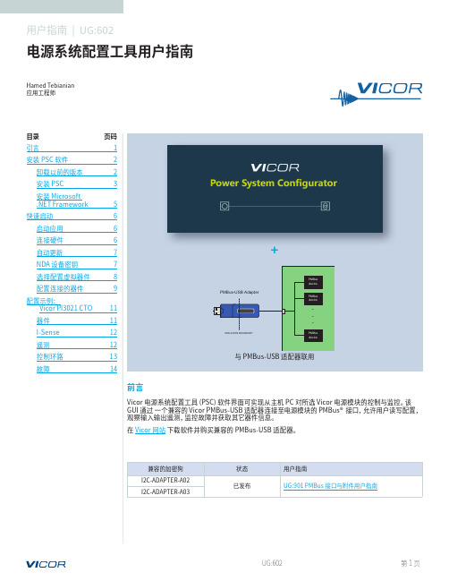
前言Vicor 电源系统配置工具 (PSC) 软件界面可实现从主机 PC 对所选 Vicor 电源模块的控制与监控。
该GUI 通过 一个兼容的 Vicor PMBus-USB 适配器连接至电源模块的 PMBus® 接口,允许用户读写配置,观察输入输出遥测,监控故障并获取其它器件信息。
在 Vicor 网站 下载软件并购买兼容的 PMBus-USB 适配器。
电源系统配置工具用户指南用户指南 | UG:602Hamed Tebianian应用工程师引言1安装 PSC 软件2卸载以前的版本 2安装 PSC 3安装 Microsoft .NET Framework 5快速启动6启动应用 6连接硬件 6自动更新7NDA 设备密钥7选择配置虚拟器件 8配置连接的器件9配置示例:Vicor PI3021 CTO11器件 11I-Sense 12遥测 12控制环路 13故障14目录页码PMBusdeviceHost PC and GUIPMBus-USB AdapterISOLATION BOUNDARYVicor Demo Board...PMBus devicePMBus device+如果窗口中没有其他版本,继续下一步, 安装 PSC:运行设置向导。
Windows 中的 添加或删除程序窗口指定文件夹地址进行安装,然后选择在这台计算机上有访问权限的用户组。
• 点击 Next >(下一步) 继续。
• 点击 Next >(下一步) 确认安装。
图 3选择安装位置和用户图 4 确认安装• 安装完成后点击 Close (关闭)。
该程序现在可从桌面或开始菜单访问。
图 6桌面名称,显示在开始菜单中• 运行下载的 .exe 并安装 .NET Framework。
• 安装完成后点击 Finish (完成)。
图 8 安装.NET Framework。
连接 PSC 与 Vicor 硬件PSC 应用程序将在启动时尝试与 Vicor 电源系统硬件连接。
HighPoint 数据RAID配置和FnL监控软件安装指南(Windows)说明书

SRD7101P/SRD7101PB /SRD7204P /SRD7104P/ SRD7104PB/SRD7140P/SRD7140PB /CRD7104PB /CRD7101PB Driver & FnL Monitor Software Installation Guide (Windows)Version v1.00Copyright © 2021 HighPoint Technologies, Inc.All rights reservedContentsOverview (1)Prerequisites for a Data-RAID Configuration (2)Installing the Device Driver (3)1.Verify that Windows recognizes the controller (3)2.Download the Device Driver (3)3.Install the Device Driver (4)Updating the Device Driver (6)1.Check the Driver version (6)2.Download the Device Driver (7)3.Shutdown and Remove the Device (7)4.Uninstall the old Device Driver (7)5.Install the new Device Driver (9)Uninstalling the Device Driver (11)Installing the FnL Management Software (FnL Monitor & CLI) (12)Uninstalling the FnL Management Software (13)Troubleshooting (15)The FnL Monitor will not start after double-clicking the desktop icon. (15)BSOD (Blue Screen of Death) (16)How to Turn off Quick Shutdown for Windows (16)Controller and Drive Detection Issues (18)Appendix (19)How to Collect Debug View Logs (19)How to Collect INF Logs (20)How to Collect System Logs (21)Collecting Windows Dump Files (22)OverviewThis guide includes important hardware/software requirements, installation & upgrade procedures, and troubleshooting tips for using SRD7101P/SRD7101PB/SRD7204P/SRD7104P/SRD7104PB/SRD7140P/ SRD7140PB/CRD7104PB/CRD7101PB NVMe AIC RAID Drives with a Windows operating system. PrerequisitesThis section describes the base hardware and software requirements for the SRD7101P/SRD7101PB/ SRD7204P/SRD7104P/SRD7104PB/SRD7140P/SRD7140PB/CRD7104PB/CRD7101PB PCIe 3.0 NVMe AIC RAID Drives.Driver InstallationThis section covers driver installation, driver upgrade and driver uninstallation procedures for SRD7101P/ SRD7101PB/SRD7204P/SRD7104P/SRD7104PB/SRD7140P/SRD7140PB/CRD7104PB/CRD7101PB NVMe AIC RAID Drives.Management Software InstallationThis section explains how to download and install the SRD7101P/SRD7101PB/SRD7204P/SRD7104P/ SRD7104PB/SRD7140P/SRD7140PB/CRD7104PB/CRD7101PB FnL Monitor Management Software S uite for Windows operating systems. The download includes both the Web RAID Management Interface (FnL Monitor), and the CLI (Command Line Interface).TroubleshootingPlease consult this section if you encounter any difficulties installing or using the SRD7101P/ SRD7204P SRD7101PB/ SRD7104P/SRD7104PB/SRD7140P/SRD7140PB/CRD7104PB/CRD7101PBNVMe AIC RAID Drives. It includes descriptions and solutions for commonly reported technical issues.AppendixA selection of useful information and web links for the SRD7101P/SRD7101PB/SRD7204P/SRD7104P/ SRD7104PB/SRD7140P/SRD7140PB/CRD7104PB/CRD7101PB NVMe AIC RAID Drives.Prerequisites for a Data-RAID ConfigurationThe SRD7101P/SRD7101PB/SRD7204P/SRD7104P/SRD7104PB/SRD7140P/SRD7140PB/CRD7104PB/CRD7101PB NVMe AIC RAID Drives can support Data-RAID arrays. In order to usera Data-RAID array, you will need the following:1. A PCIe 3.0 slot with x8 or x16 lanes. The SRD7104P/SRD7104PB/SRD7101P/SRD7101PB/SRD7140P/SRD7140PB/CRD7104PB/CRD7101PB must be installed into a PCIe 3.0 slot with x16 dedicated lanes, The SRD7204P can be installed into a PCIe 3.0 x8 or x16 slot.2.Make sure any non-HighPoint drivers are uninstalled for any SSD’s hosted by the FnLseries RAID controllers. 3rd party software and manufacturer provided drivers may prevent the FnL from functioning properly.Warnings:1)Failing to remove the AIC Drive and SSD’s when uninstalling the driver may result in dataloss.2)Always make sure the FnL driver is installed before moving a FnL series NVMe AIC RAIDDrives & RAID array to another Windows system.Windows operating systems will always load the default NVMe support after the FnL driver has been uninstalled, or if it detects the present of a card when no driver has been loaded – this driver will only recognize the NVMe SSD’s as separate disks.If the SSD’s are recognized separately, any data they contain may be lost – this includes RAIDconfiguration data.Installing the Device DriverThe following section discusses driver installation for a non-bootable NVMe configuration.1.Verify that Windows recognizes the controllerAfter installing the FnL controller into the motherboard, power on the computer, boot the Windows operating system, and open Device Manager.A.Expand the Disk drives tab. Each NVMe SSD’s installed into the SRD7101P/SRD7101PB/SRD7204P/SRD7104P/SRD7104PB/SRD7140P/SRD7140PB/ CRD7104PB/CRD7101PBcontroller should be displayed here.B.Expand the Storage Controllers tab. You should see a “Standard NVM Express Controller”entry for each NVMe SSD that is installed into the AIC RAID Drive.Example screenshot SRD7104:AB2.Download the Device DriverDownload the appropriate FnL driver from the NVMe AIC RAID Drives Software Downloads webpage.SRD7101P/SRD7101PB:https:///srd7101p-overviewSRD7104P/SRD7104PB:https:///srd7104p-overviewSRD7204P:https:///srd7204p-overviewSRD7140P/SRD7140PB:https:///srd7140p-overviewCRD7101PB:https:///crd7101pb-overviewCRD7104PB:https:///crd7104pb-overview3.Install the Device DriverA.Locate the driver download and open the file.B.Double-click setup.Note: If installation does not start, you may have to manually start setup using AdministratorPrivileges. Right-click setup, select Run as Administrator from the menu, and confirm the pop-up window to proceed.After driver installation is complete, click OK to reboot.C.Once Windows has rebooted, open Device Manager to check the status of the driver.Expand Storage controllers and click on the HighPoint NVMe RAID Controller entry. View the properties and click the Driver tab:Example screenshot (SRD7104)Note: The driver revision shown in the screenshots may not correspond with current software releases. Please make sure to download the latest driver updates from the product’s Software Updates page.D.First, make sure the FnL Monitor has been installed (see FnL Monitor install). Open the FnLMonitor and make sure the SSD.’s / arrays are properly recognized.Note: Please refer to Appendix A to verify that your Device Manager entries correspond with the driver version you have installed.Updating the Device DriverNote: Before attempting to update the driver entry, ensure that the AIC RAID Drive is removed from the motherboard.1.Check the Driver versionOpen Device Manager to check the current driver version. Expand Storage controllers and click on the HighPoint NVMe RAID Controller entry. View the properties and click the Driver tab:Example screenshot (SRD7104)2.Download the Device DriverDownload the latest driver from the controller’s Software Downloads webpage.SRD7101P/SRD7101PB:https:///srd7101p-overviewSRD7104P/SRD7104PB:https:///srd7104p-overviewSRD7204P:https:///srd7204p-overviewSRD7140P/SRD7140PB:https:///srd7140p-overviewCRD7101PB:https:///crd7101pb-overviewCRD7104PB:https:///crd7104pb-overview3.Shutdown and Remove the DeviceA.Power down the system and remove the NVMe AIC RAID Drives from the motherboard.Note: Failing to remove the FnL controller from the motherboard during the uninstall process may result in data loss.Whenever the driver is uninstalled, Windows will attempt to install the default NVMe support,which may corrupt the RAID configurations and any data stored on SSD’s hosted by the FnLcontroller.B.Power on the system and boot Windows.4.Uninstall the old Device DriverA.Access Control Panel and select Programs→ Programs and Features, and click on the HighPointNVMe Driver entry.B.Click Uninstall/ChangeIf the HPT controller is not removed from the motherboard during the uninstall process, Windows will notify you that RAID data may be destroyed.C.After uninstalling the driver, click OK to reboot.D.After Windows has rebooted, access Control Panel to make sure the driver has been uninstalled.If there are no HighPoint NVMe RAID Driver entries present, the driver has been successfully uninstalled:5.Install the new Device DriverA.Locate the driver download and open the file.B.Double-click setup.Note: If the update does not start, you may have to manually start setup using AdministratorPrivileges. Right-click setup, select Run as Administrator from the menu, and confirm the pop-up window to proceed.C.Windows will notify you that the driver is already installed. Click OK to reboot.D.After entering the system, shut down the system.In the shutdown state, connect the FnLcontroller to the motherboard.E.Boot into the system.F.Once Windows has rebooted, open Device Manager to check the status of the driver. ExpandStorage controllers and click on the HighPoint NVMe RAID Controller entry. View theproperties and click the Driver tab:Note: The driver revision shown in the screenshots may not correspond with current software releases. Please make sure to download the latest driver updates from the product’s Software Updates page.G.First, make sure the FnL Monitor has been installed (see FnL Monitor install). Open the FnLMonitor and make sure the SSD.’s / arrays are properly recognized.For Example: SRD7204Uninstalling the Device Driver1.Power down the system and remove the NVMe AIC RAID Drives from the motherboard.Note: Failing to remove the FnL controller from the motherboard during the uninstall process may result in data loss. Whenever the driver is uninstalled, Windows will attempt to install the default NVMe support, which may corrupt the RAID configurations and any data stored on SSD’s hosted by the FnL controller.2.Power on the system and boot Windows.3.Access Control Panel and select Programs→ Programs and Features, and click on the HighPointNVMe Driver entry.4.Click Uninstall/Change5.After uninstalling the driver, click OK to reboot.6.After Windows has rebooted, access Control Panel to make sure the driver has been uninstalled. Ifthere are no HighPoint NVMe RAID Driver entries present, the driver has been successfullyuninstalledInstalling the FnL Management Software (FnL Monitor & CLI)The HighPoint FnL Management Software (FnL Monitor and CLI utilities) are used to monitor NVMe SSD’s hosted by the NVMe AIC RAID Drives. Download the latest software package from the HighPoint website:SRD7101P/SRD7101PB:https:///srd7101p-overviewSRD7104P/SRD7104PB:https:///srd7104p-overviewSRD7204P:https:///srd7204p-overviewSRD7140P/SRD7140PB:https:///srd7140p-overviewCRD7101PB:https:///crd7101pb-overviewCRD7104PB:https:///crd7104pb-overview1.Extract the package and double-click the FnL Monitor program to install the software.2.Once installed, locate the Management icon on the desktop and double-click to start the FnL Monitorinterface.Uninstalling the FnL Management Software1.Access Control Panel and select Programs→ Programs and Features, and click on the FnL Monitorentry.2.Click Uninstall/Change3.After uninstalling the driver, click Finish.TroubleshootingNote: When troubleshooting your NVMe AIC RAID Drives, make sure all of the Prerequisites have been met before proceeding.The FnL Monitor will not start after double-clicking the desktop icon.1.This is often the result of a missing driver or improperly installed driver. Open Device Managerand check under Storage Controllers.If the Driver is properly installed, you should see a HighPoint NVMe Controller entry forNVMe AIC RAID Drives, followed by HighPoint NVMe RAID Controller entry:Example screenshot (SRD7104)Note: The driver revision shown in the screenshots may not correspond with current software releases.Please make sure to download the latest driver updates from the product’s Software Updates page.2.You should also check to make sure hptsvr is running under Task Management → Services. Ifthe status of hptsvr process is Stopped, right-click on this entry and select Start from the menu:BSOD (Blue Screen of Death)There are three scenarios in which a BSOD may occur with AIC RAID DriveWindows displays a BSOD when the AIC RAID Drive is installed.If you are running Windows 10, please make sure that any Quick Shutdown options are disabled – these features can cause a BSOD when the AIC RAID Drive is installed into or removed from your motherboard. BSODs can be avoided by completely powering off your system.How to Turn off Quick Shutdown for Windowse administrator privileges to access the Command Prompt utility:b.Enter the following command and press Enter:powercfg / h offc.To make sure the setting has been disabled, enter the following command and pressEnter:powercfg / ad.Shut down the computer and remove the AIC RAID Drive from the motherboard;e.Restart the system and open the SRD7101P/SRD7101PB/SRD7204P/SRD7104P/SRD7104PB/SRD7140P/SRD7140PB/CRD7104PB/CRD7101PB driver download.f.Double-click Setup to reinstall the driver; if you are prompted to uninstall the driver, youwill need to follow the prompts and restart. After rebooting, double-click Setup once more to install the driver.After the driver installation is complete, shut down the computer. The AIC RAID Drive insert into the motherboard PCIe slot.g.Power on the system, boot Windows and access the FnL Monitor; if the FnL Monitorcan't connect, you need to restart again.h.If it fails to start the second time, please access our Online Support portal and submit asupport ticket.Note:If you are running a Server version of windows, and encounter a BSOD at bootup,please collect the following information: Windows version & build numbers, MemoryDump and System event Log1. A BSOD is encountered when installing the driver:If you experience a BSOD during driver installation, please collect the following information:Memory Dump, INF log, Debug Log, System Event log, and submit a new support ticket via our Online Support Portal.2.If Windows reports that driver installation has failed:a.Please collect these debugging information: INF log, Debug Log, DeviceManager/Storage Controller screen shot, System Event logNote:If you experience a BSOD or error when installing the driver, please ensure that any Quick Shutdown options are not enabled– Quick shutdown can cause a BSOD when removing theAIC RAID Drive from your motherboard, and plugging it back in. BSODs can be avoided bycompletely powering off your system:Controller and Drive Detection Issues•If your motherboard or Windows is unable to detect the NVMe AIC RAID Drives or NVMe SS D’s, please shutdown the system and try moving the NVMe AIC RAID Drives to another PCIeslot.•Make sure any unrelated NVMe devices are removed from the motherboard while troubleshooting the SRD7101P/SRD7101PB/SRD7204P/SRD7104P/SRD7104PB/SRD7140P/SRD7140PB/CRD7104PB/CRD7101PB NVMe AIC RAID Drives.AppendixHow to Collect Debug View LogsIf other troubleshooting steps fail to solve the problem, we suspect that the driver and management softwa re cannot establish a connection with the SRD7101P/SRD7101PB/SRD7204P/SRD7104P/SRD7104PB/ SRD7140P/SRD7140PB/CRD7104PB/CRD7101PB NVMe AIC RAID Drives. We will provide you with a Debug version of the driver to collect information about the problem you areexperiencing.To install the Debug driver, follow the standard driver installation procedure (please refer to theSRD7101P/SRD7101PB/SRD7204P/SRD7104P/SRD7104PB/SRD7140P/SRD7140PB/CRD7104PB/ CRD7101PB NVMe AIC RAID Drives User Guide). After installing the driver, follow the steps below:1.Download the DebugView utility from https:///files/DebugView.zip.2.Unzip, right-click on the icon, and run DebugView with administrator privileges. Select CaptureWin32, Capture Kernel, Enable Verbose Kernel Output, and Pass in the Capture toolbar.3.If the utility displays an “access denied” message, rename the following file:C:\Windows\System32\drivers\Dbgv.sys For example, rename it to “Dbgv.sys1”, i.e change the file type.4.Save the information printed by DebugView and send this to our support department.5.If required, we will provide management software information collection tools for the NVMeRAID Manager interface.How to Collect INF Logs1.Go to drive C→ Windows→ INF, and locate the setuppapi.dev and setupapi.setup logs:INF logs can be used to check what kind of software has been installed into the Windowssystems.2.Please access Device Manager, Storage Controllers, and check the properties for the HighPointentry. Click on Driver Details and take a screenshot – include this with the log files you submit for your support case.How to Collect System LogsIn addition to DebugView logs, System Logs can aid our Support department diagnose and resolve the support issues you have submitted. The System Log typically records errors, device failures, and software or driver related incidents. This information can help our engineers narrow down or even identify the source of the problem you are experiencing.System Log1.Click the Windows button towards the bottom left-hand corner of your desktop, and click on theSearch field.2.Type Event Viewer and click the icon as shown below:3.Expand the Windows Log folder and select System:4.Select Save All Events as… and save the .evtx file in an easy to find location.Collecting Windows Dump FilesWindows Dump files are snap shots that show which processes were running at the time of the event or failure. If possible, locate and upload the following files to your support case:•Memory.dmp•Minidump.dmpTo locate the dump files, check the C:\Windows directory and search for Memory.dmp andMinidump.dmp:。
大屏兼容表
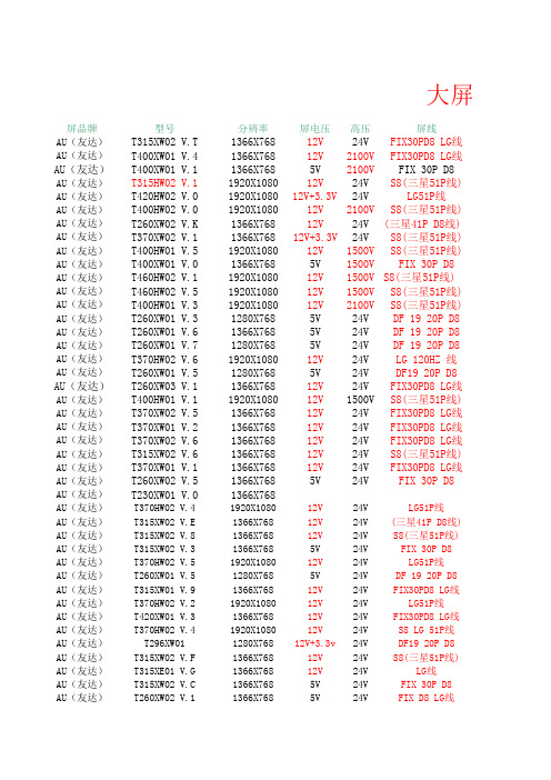
大屏兼屏品牌型号分辨率屏电压高压屏线AU(友达)T315XW02 V.T1366X76812V24V FIX30PD8 LG线AU(友达)T400XW01 V.41366X76812V2100V FIX30PD8 LG线AU(友达)T400XW01 V.11366X7685V2100V FIX 30P D8AU(友达)T315HW02 V.11920X108012V24V S8(三星51P线)AU(友达)T420HW02 V.01920X108012V+3.3V24V LG51P线AU(友达)T400HW02 V.01920X108012V2100V S8(三星51P线)AU(友达)T260XW02 V.K1366X76812V24V(三星41P D8线)AU(友达)T370XW02 V.11366X76812V+3.3V24V S8(三星51P线)AU(友达)T400HW01 V.51920X108012V1500V S8(三星51P线)AU(友达)T400XW01 V.01366X7685V1500V FIX 30P D8AU(友达)T460HW02 V.11920X108012V1500V S8(三星51P线)AU(友达)T460HW02 V.51920X108012V1500V S8(三星51P线)AU(友达)T400HW01 V.31920X108012V2100V S8(三星51P线)AU(友达)T260XW01 V.31280X7685V24V DF 19 20P D8AU(友达)T260XW01 V.61366X7685V24V DF 19 20P D8AU(友达)T260XW01 V.71280X7685V24V DF 19 20P D8AU(友达)T370HW02 V.61920X108012V24V LG 120HZ 线AU(友达)T260XW01 V.51280X7685V24V DF19 20P D8AU(友达)T260XW03 V.11366X76812V24V FIX30PD8 LG线AU(友达)T400HW01 V.11920X108012V1500V S8(三星51P线)AU(友达)T370XW02 V.51366X76812V24V FIX30PD8 LG线AU(友达)T370XW01 V.21366X76812V24V FIX30PD8 LG线AU(友达)T370XW02 V.61366X76812V24V FIX30PD8 LG线AU(友达)T315XW02 V.61366X76812V24V S8(三星51P线)AU(友达)T370XW01 V.11366X76812V24V FIX30PD8 LG线AU(友达)T260XW02 V.51366X7685V24V FIX 30P D8AU(友达)T230XW01 V.01366X768AU(友达)T370HW02 V.41920X108012V24V LG51P线AU(友达)T315XW02 V.E1366X76812V24V(三星41P D8线)AU(友达)T315XW02 V.81366X76812V24V S8(三星51P线)AU(友达)T315XW02 V.31366X7685V24V FIX 30P D8AU(友达)T370HW02 V.51920X108012V24V LG51P线AU(友达)T260XW01 V.51280X7685V24V DF 19 20P D8AU(友达)T315XW01 V.91366X76812V24V FIX30PD8 LG线AU(友达)T370HW02 V.21920X108012V24V LG51P线AU(友达)T420XW01 V.31366X76812V24V FIX30PD8 LG线AU(友达)T370HW02 V.41920X108012V24V S8 LG 51P线AU(友达)T296XW011280X76812V+3.3v24V DF19 20P D8AU(友达)T315XW02 V.F1366X76812V24V S8(三星51P线)AU(友达)T315XE01 V.G1366X76812V24V LG线AU(友达)T315XW02 V.C1366X7685V24V FIX 30P D8AU(友达)T260XW02 V.11366X7685V24V FIX D8 LG线AU(友达)T315XW02 V.61366X76812V24V S8(三星51P线) AU(友达)T260XW02 V.L1366X76812V24V FIX30PD8 LG线AU(友达)T315XW02 V.D1366X76812V24V FIX30PD8 LG线AU(友达)T315XW02 V.M1366X76812V24V FIX30PD8 LG线AU(友达)T420XW01 V.2 XXXXG 1366X76812V24V三星51P线 S8 AU(友达)T420XW01 V.3 1366X76812V24V FIX30PD8 LG线AU(友达)T420XW01 V.61366X76812V24V三星51P线 S8 AU(友达)T420XW01 V.41366X7685V24V FIX30PD8 LG线AU(友达)T370HW02 V.11920X108012V24V LG51P线AU(友达)T315XW02 V.L xxxxg1366X76812V24V FIX 30P D8 AU(友达)T315XW02 V.L 1366X76812V24V FIX30PD8 LG线AU(友达)T315XW02 V.11366X7685V24V FIX 30P D8 AU(友达)T420XW01 V.01366X76812V24V FIX30PD8 LG线AU(友达)T315HW02 V.01920X108012V24V三星51P线 S8 AU(友达)T420XW01 V.81366X76812V24V FIX30PD8 LG线AU(友达)T400HW02 V.11920X108012V24V三星51P线 S8 AU(友达)T260XW03 V.0 1366X7685V24V FIX 30P D8 AU(友达)T315XW02 V.K1366X76812V24V三星41P线 D8 AU(友达)T315XW01 V.01366X7685V24V FIX 30P D8 AU(友达)T420XW01 V.51366X76812V24V FIX30PD8 LG线AU(友达)T370HW01 V.11920X108012V24V FIS41HS8线AU(友达)T315XW02 V.01366X76812V24V三星51P线 S8 AU(友达)T260EW01 V.21280X76812V24V DF14 20P D8 AU(友达)T460HW02 V.41920X108012V1000V S8(三星51P线) AU(友达)T460HW03 V.31920X108012V1000V三星120HZ屏线AU(友达)T315HW02 V.71920X108012V24V S8(三星51P线) AU(友达)T460HW03 V.21920X108012V24V S8(三星51P线) AU(友达)T460HW03 V.11920X108012V24V S8(三星51P线) AU(友达)T315XW03 V.D1366X76824FFC 30PD8T460HW081920X10801224LG51P线 S8三星LTY320HA031920X108012V24V三星 51P 三星LTA230W1-L051366X7685V24V FIX 30P D8三星LTA400HT-L011920X108012V1500V三星51P 三星LTY460HB081920X108012V1500V三星51P 三星LTA320WT-L061366X7685V24V FIX 30P D8三星LTA320WT-L071366X7685V24V FIX 30P D8三星LTA260W1-L031280X7685V15V DF14 30P D8线三星LTA260W1-L051280X7685V24V D8三星LTA460HS-L021920X108012V24V S8三星LTA400WT-L171920X108012V24V D8三星LTM201M1-L011680X105012V12V S8三星LTA460WT-L141366X76812V24V D8三星LTA400W1-L021280X7685V120V D8三星LTI400WT-L021366X76812V24V D8三星LTA320WT-L061366X7685V24V D8三星LTA400WT-L011280X7685V120V D8三星LTA400WS-L021366X7685V24V D8三星LTY400HS-LH31920X108012V24V S8三星LTA520HB091920X108012V24V S8(51P)三星LTA460HT-L031920X108012V24V S8(51P)三星LTA460HT-LH31920X10805V24V S8(51P)三星LTI460WT-L171366X7685V24V FIX 30P D8三星LTI460WT-L021366X76812V24V FIX 30P D8三星LTI460HS-L031920X108012V24V三星 51P三星LTA400W2-L031366X7685V24V FTX 30P D8三星LTI400HS-L021920X108012V24V三星51P三星LTA460WT-L031366X7685V24V FTX 30P D8三星LTA460WS-L031366X7685V24V FTX 30P D8三星LTY520HE031920X108012V三星120HZ屏线三星LTY320HA011920X108012V24V三星51P三星LTZ320WH-LH21366X76812V24V三星51P三星LTZ400HA031920X108012V24V三星51P三星LTA320AB011366X76812V24V FTX 30P D8三星LTA400WT-L111366X7685V24V FTX 30P D8三星LTY460HT-LH11920X10805V三星51P三星LTY400WT-LH31366X76812V1500V三星41P线 D8三星LTY400HC011920X108012V2100V三星120HZ线三星LTZ400HA071920X108012V2100V三星51P三星LTA400HF02_HD1920X108012V24V三星120HZ线夏普LQ315T3LZ131366X7685V12V D8夏普LQ255T3LZ2J1366X7685V12V LG线夏普LK370D3LZ171920X108012V24V S8(FIX)夏普LK370T3LZ5BW1366X7685V24V FIX30PD8(LG线)夏普LK370D3LZ1AY1920X108012V24V V420(两个头)41P 夏普LK260T3LF141366X7685V24V FIX30PD8(LG线)奇美V420H1-LH41920X108012V24V LG120HZ线奇美V315B1-L091366X76812V24V FIX30PD8(LG线)奇美V315B1-L081366X76812V24V FIX30PD8(LG线)奇美V400H1-L011920X108012V2100V三星51P奇美V400H1-L011920X108012V24V三星51P奇美V420H1-L131920X108012V24V LG51P S8奇美V260B1-L111366X76812V24V D8奇美V420B1-L041366X7685V24V D8(LG线)奇美V320B1-L051366X76812V24V D8(LG线)奇美V420H1-L121920X108012V24V S8 LG51P 奇美V315B1-L011366X7685V24V FIX 30P D8奇美V315B1-L051366X76812V24V FIX30PD8 LG线奇美V420B1-L041366X7685V24V FIX30PD8 LG线奇美V270B1-L011366X7685V24V V320B1线奇美V260B1-L041366X7685V24V FIX 30P D8奇美V420H1-L051920X108012V24V S8奇美V420B1-L011366X76812V24V D8奇美V420H1-L111920X108012V24V S8奇美V470H1-L031920X108012V24V LG51P S8奇美V260B1-L031366X76812V24V LG线奇美 V315B3-L04 1366X768 12V 24V FIX 30P D8奇美V270B1-L03 1366X7685V24V V320B1线奇美V320B1-L01 1366X7685V24V V320B1线奇美V320B1-L061366X7685V24V V320B1线奇美V270B1-L011366X7685V24V V320B1线奇美V270W1-L031280X7205V24V V270线DF1430PD8奇美V470H1-L021920X108012V24V LG51P S8奇美V320B1-L041366X7685V24V V320B1线奇美V260B1-L011366X7685V24V FIX 30P D8 QD QD32HL011366X7685V24V FIX 30P D8 QD QD32HL0311366X76812V24V FIX 30P D8UD UD320XD1366X7685V24V V320B1线LG LC370WUN1920X108012V+3.3v24V LG51P线LG LC370WU31920X1080LG LC200WX11366X76812V24V D8LG LC260WX21366X76812V24V D8LG LC320W011366X76812V24V D8LG LM240WU2(SLA1)1920X120012V+3.3v24V FIX 30P S8 LG LM240WU2(SLB1)1920X120012V24V FIX 30P S8 LG LC420WU61920X108012V24V S8 LG51PLG LC320WX1(SL)(B1)1366X76812V+3.3v24V S8 LG51PLG LC320WXD(SA)(C1)1366X76812V+3.3v24V S8 LG51PLG LC420WUN1920X108012V+3.3v24V S8 LG51PLG LM240WU3 (TL)(C1)1920X12005V24V FIX 30P S8 LG LC260WX2(SL)(02)1366X7685V24V FIX30PD8 LG线LG LC470WU5(SL)(A2)1920X108012V+3.3v24V S8 LG51PLG LC420WUE1920X108012V+3.3v24V S8 LG51PLG LC260W01(A5)(K6)1280X76812V24V DF14 20P D8 LG LC370WU2(SL)(A2)1920X108012V24V LG 120HZ 线LG LC420WU5(SL)(A1)1920X108012V24V S8 LG51PLG LC320WUN1920X108012V+3.3v24V LG51P线LG LC420WUD1920X108012V24V120HZ线LG LM260WU11920X120012V24V FIX 30P S8日立TX66D11VCOCAB1366X76812V24V FIX30PD8 LG线中华中华中华CLAA370WF02 CZ(CPT)1366X76812V24V FIX 30P D8 中华CLAA370WA03 SCD1366X76812V24V FIX30PD8(LG线)中华CLAA370WF02 S Z1366X76812V24V FIX 30P D8中华CLAA370WA03 SC1366X76812V24V FIX30PD8(LG线)中华CLAA320WF01 UX1366X76812V24V FIX 30P D8中华CLAA320WF01 UZ1366X76812V24V FIX 30P D8中华CLAA370WA03 SCZ1366X76812V24V FIX30PD8(LG线)中华CLAA320WF01 UD1366X76812V24V FIX 30P D8中华CLAA370WA03 1366X76812V24V FIX30PD8(LG线)中华CLAA370WA021366X76812V24V跳线中华CLAA320WA01CV1366X76812V24V跳线中华CLAA320WF01 SC1366X76812V24V FIX 30P D8大屏兼容表备注正程序正程序 电源:IP-2311135B正程序 电源:IP-2311135BT400HW01_V.3程序屏线倒数第七脚加3.3V 奇偶反 MAP反程序T400HW01 V.3程序 三星电源2100V 电源型号:IP-231135A6E18:MAP反屏线倒数第七脚加3.3V(电源为1脚)正程序正程序 电源SIP400B正程序 电源SIP400B正程序 电源:IP-301135A (高压点两边)电源:IP-301135A (电源高压输出用单口点,左右各一个)6E18:MAP反(专用程序 )电源型号: IP-231135A正程序正程序正程序正程序正程序正程序 电源SIP400B HV1接最上边脚位 HV2接最下边脚位正程序正程序正程序6E18:MAP反正程序正程序电源地线中间加100R电阻6E18:奇偶反程序6E18:MAP反6E18:MAP反正程序6E18:奇偶反程序正程序正程序6E18:奇偶反程序正程序6E18:奇偶反程序屏接口倒数第三脚接3.3V,最后一脚接地(由左至右数起) MAP反程序(S8L_1366X768 120HZ) 6E18:MAP反正程序6E18:MAP反正程序正程序正程序6E18:MAP反正程序6E18:MAP反6E18:MAP反6E18:奇偶反程序正程序正程序正程序正程序正程序正程序6E18:MAP反 (专用程序)正程序正程序正程序6E18:MAP反正程序黄色46电源,高压两边各点一条线黄色46电源,高压两边各点一条线 小板写U4程序 34 12正程序正程序正程序正程序MAP反程序高压12脚同14脚连起MAP反程序 电源:SIP400BMAP反程序 电源:IP-301135A正程序正程序4P脚位定义:第一脚地线,开关第四脚,接地线,(由高至低数起)高压开关12脚,亮度13脚(第二个口,开关位,由高至低数)第一个口接电源地线14P脚位定义: 5:地 8:5V 14:开关(由高至低数起)14P脚位定义: 5:地 8:5V 14:开关(由高至低数起)6E18:MAP反6E18:MAP反6E18:MAP反6E18:MAP反6E18:MAP反6E18:MAP反6E18:MAP反6E18:MAP反双包52电源,反馈线:PROT1接LD,IL1接FB EY21:左接上,右接下 EY22:左接上,右接下6E18:MAP反6E18:MAP反 S8L 1366X7686E18:MAP反6E18:MAP反 亮度线13脚6E18:MAP反 三星电源2100V 电源型号:IP-231135A6E18:MAP反 1500V电源6E18:MAP反 1500V电源:SIP400D电源:IP-231135AMAP反程序 电源:IP-231135ALED自带电源。
- 1、下载文档前请自行甄别文档内容的完整性,平台不提供额外的编辑、内容补充、找答案等附加服务。
- 2、"仅部分预览"的文档,不可在线预览部分如存在完整性等问题,可反馈申请退款(可完整预览的文档不适用该条件!)。
- 3、如文档侵犯您的权益,请联系客服反馈,我们会尽快为您处理(人工客服工作时间:9:00-18:30)。
Product Description: T315HW02 TFT-LCD PANEL with RoHS guaranteeAUO Model Name: T315HW02 V7Customer Part No/Project Name:Customer Signature Date AUO 2008/5/10Approved By: PM Director / Frank HsuReviewed By: RD Director / Eugene CC ChenReviewed By: Project Leader / Samuel FuPrepared By: PM / Hanson WangDocument Version : 0.0Date : 2009/05/10Product Specifications 31.5” FHD Color TFT-LCD ModuleModel Name: T315HW02 V7(*) Preliminary Specifications() Final SpecificationsContents NoCOVERCONTENTSRECORD OF REVISIONS1 GENERAL DESCRIPTION2 ABSOLUTE MAXIMUM RATINGS3 ELECTRICAL SPECIFICATIONS3-1 ELECTRICAL CHARACTREISTICS3-2 INTERFACE CONNECTIONS3-3 SIGNAL TIMING SPECIFICATIONS3-4 SIGNAL TIMING WAVEFORMS3-5 COLOR INPUT DATA REFERNECE3-6 POWER SEQUENCE4 OPTICAL SPECIFICATIONS5 MECHANICAL CHARACTERISTICS6 RELIABLITY7 INTERNATIONAL STANDARDS8 PACKING9 PRECAUTIONSVersion Date No Old Description New Description Remark0 2009/2/19 First issue0.1.General DescriptionThis specification applies to the 31.5 inch Color TFT-LCD Module T315HW02 V7. This LCD module has a TFT active matrix type liquid crystal panel 1920x1080 pixels, and diagonal size of 31.5 inch. This module supports 1920x1080 HDTV mode (Non-interlace).Each pixel is divided into Red, Green and Blue sub-pixels or dots which are arranged in vertical stripes. Gray scale or the brightness of the sub-pixel color is determined with a 8-bit gray scale signal for each dot.The T315HW02 V7 has been designed to apply the 8-bit 1 channel LVDS interface method. It is intended to support displays where high brightness, wide viewing angle, high color saturation, and high color depth are very important.The T315HW02 V7 model is RoHS verified which can be distinguished on panel label.* General InformationItems Specification Unit NoteActive Screen Size 31.55 inchesDisplay Area 698.4 (H) x 392.85 (V) mmOutline Dimension 760.0(H) x 450.0(V) x 45(D) mm With inverterDriver Element a-Si TFT active matrixDisplay Colors 16.7M ColorsNumber of Pixels 1920x1080 PixelPixel Pitch 0.36375 mmPixel Arrangement RGB vertical stripeDisplay Mode Normally BlackSurface Treatment AG, 3H Haze = 11%2.Absolute Maximum RatingsThe following are maximum values which, if exceeded, may cause permanent damage to the unit.Item Symbol Min Max Unit Conditions Logic/LCD Drive Voltage Vcc -0.3 14 [Volt] Note 1Input Voltage of Signal Vin -0.3 3.6 [Volt] Note 1BLU Input Voltage VDDB -0.3 28 [Volt] Note 1BLU Brightness Control Voltage Vdim -0.3 7.0 [Volt] Note 1Operating Temperature TOP 0 +50 [o C] Note 2Operating Humidity HOP 10 90 [%RH] Note 2Storage Temperature TST -20 +60 [o C] Note 2Storage Humidity HST 10 90 [%RH] Note 2Panel Surface Temperature PST 65 [o C] Note 3Note 1: Duration:50 msec.Note 2 : Maximum Wet-Bulb should be 39 and No condensation.℃The relative humidity must not exceed 90% non-condensing at temperatures of 40or less. At temperatures greater℃than 40, the wet bulb temperature must not exceed 39.℃℃Note 3: Surface temperature is measured at 50℃Dry condition3. Electrical SpecificationThe T315HW02 V7 requires two power inputs. One is employed to power the LCD electronics and to drive the TFT array and liquid crystal. The second input power for the BLU, is to power inverter..3-1 Electrical CharacteristicsParameterValuesMinTypMaxUnitNotesCD:Power Supply Input Voltage Vcc 10.8 12 13.2 Vdc 1 Power Supply Input Current Icc - 0.65 0.75 A 2 Power Consumption Pc - 7.8 9 Watt 2 Inrush CurrentI RUSH - - 6 Apeak 3 Differential Input High Threshold VoltageVTH100 mV4Differential Input Low Threshold VoltageVTL -100 mV 4 LVDS InterfaceCommon Input Voltage VCIM 1.10 1.25 1.40 V 4 Input High Threshold VoltageVIH (High) 2.43.3VdcCMOS InterfaceInput Low Threshold VoltageVIL (Low) 0 0.7 Vdc Life Time50,000Hours6Note :1. The ripple voltage should be controlled under 10% of V CC2. Vcc=12.0V ,=v f 60Hz, fCLK=81.5Mhz , 25, Test Pattern : White Pattern ℃3. Measurement condition :4. VCIM = 1.2V5. The performance of the Lamp in LCD panel, for example life time or brightness, is extremely influenced by thecharacteristics of the DC-AC Inverter. So all the parameters of an inverter should be carefully designed as not to produce too much leakage current from high-voltage output of the inverter. When you design or order the inverter, please make sure unwanted lighting caused by the mismatch of the lamp and the inverter (no lighting, flicker, etc) never occurs. After confirmation, the LCD panel should be operated in the same condition as installed in your instrument.6. Do not attach a conducting tape to lamp connecting wire. If the lamp wire attach to conducting tape, TFT-LCDModule have a low luminance and the inverter has abnormal action because leakage current occurs between lamp wire and conducting tape.7. The relative humidity must not exceed 80% non-condensing at temperatures of 40 or less. At temperatures℃greater than 40, the wet bulb temperature must not exceed 39. When operate at low temperatures, the ℃℃brightness of CCFL will drop and the life time of CCFL will be reduced.0V3-2 Interface Connections-Connector on Panel: JAE FI-RE51S-HF(Manufactured by JAE)-Note:1.All GND (ground) pins should be connected together and should also be connected to the LCD’s metal frame.All Vcc (power input) pins should be connected together.2.For Pin 10, 27 and 28, panel will not damage if negligently connect these pins to high or lowLVDS Option = High/Open, NS modeOR0OG0OR5OR4OR3OR2OR1OR0OG0OG1OB1OB0OG5OG4OG3OG2OG1OB1OB2DEVS HS OB5OB4OB3OB2OR6OB7OB6OG7OG6OR7OR6ER0EG0ER5ER4ER3ER2ER1ER0EG0EG1EB1EB0EG5EG4EG3EG2EG1EB1EB2EB5EB4EB3EB2DEER6EB7EB6EG7EG6ER7ER6ORXCLK+ORXCLK-ORX0ORX1ORX2ORX3ERXCLK+ERXCLK-ERX0ERX1ERX2ERX3DEVS HSNote:Odd data is the first priority. First data is odd.LVDS Option = Low (0V) , JEIDA modeOR2OG2OR7OR6OR5OR4OR3OR2OG2OG3OB3OB2OG7OG6OG5OG4OG3OB3OB4DEVS HS OB7OB6OB5OB4OR0OB1OB0OG1OG0OR1OR0ER2EG2ER7ER6ER5ER4ER3ER2EG2EG3EB3EB2EG7EG6EG5EG4EG3EB2EB4EB7EB6EB5EB4DEER0EB1EB0EG1EG0ER1ER0ORXCLK+ORXCLK-ORX0ORX1ORX2ORX3ERXCLK+ERXCLK-ERX0ERX1ERX2ERX3DEVS HS3-3 Signal Timing SpecificationsThis is the signal timing required at the input of the User connector. All of the interface signal timing should be satisfied with the following specifications for it’s proper operation. * Timing Table DE only Mode Vertical Frequency: Signal Vertical Section Item Period Active Blanking Period Horizontal Section LVDS Clock Vertical Frequency Horizontal Frequency Active Blanking Symbol Tv Tdisp(v) Tblk (v) Th Tdisp(h) Tblk (h) 70 50 47 10 1030 Min. 1090 Typ. 1125 1080 45 1100 960 140 74.25 60 365 82 63 400 1325 Max. 1480 Unit Th Th Th Tclk Tclk Tclk MHz HzFrequency Fclk (1/Tclk) Frequency FvFrequencyFh6067.573kHzNotes: 1.) Di splay position is specific by the rise of DE signal only. Horizontal display position is specified by the falling edge of 1st DCLK right after the rise of ENAB, is displayed on the left edge of the screen. Vertical display position is specified by the rise of DE after a “Low” level period equivalent to eight times of horizontal period. The 1st data corresponding to one horizontal line after the rise the of ENAB is displayed at the top line of screen. 3.) If a period of DEB “High” is less than 1920 DCLK or less than 1080 lines, the rest of the screen displays black. 4.) The display position does not fit to the screen if a period of DE “High” and the effective data period do not synchronize with each other.Copyright AU Optronics, Inc. January, 2009 All Rights Reserved. 11/29 No Reproduction and Redistribution Allowed◎T315HW02 V7 - Spec. Ver 0.13-4 Signal Timing WaveformsCopyright AU Optronics, Inc. January, 2009 All Rights Reserved. 12/29 No Reproduction and Redistribution Allowed◎T315HW02 V7 - Spec. Ver 0.13-5 Color Input Data ReferenceThe brightness of each primary color (red, green and blue) is based on the 8 bit gray scale data input for the color; the higher the binary input, the brighter the color. The table below provides a reference for color versus data input.COLOR DATA REFERENCEInput Color Data Color MSB RED LSB MSB GREEN LSB MSB BLUE LSBR7 R6 R5 R4 R3 R2 R1 R0 G7 G6 G5 G4 G3 G2 G1 G0 B7 B6 B5 B4 B3 B2 B1 B0 Black Red(255) Green(255) Basic Color Blue(255) Cyan Magenta Yellow White RED(000) RED(001) RED ---RED(254) RED(255) 1 1 1 1 0 0 1 1 0 0 1 1 0 0 1 1 0 0 1 1 0 0 1 1 0 0 0 1 0 0 0 0 0 0 0 0 0 0 0 0 0 0 0 0 0 0 0 0 0 0 0 0 0 0 0 0 0 0 0 0 0 1 0 0 0 0 0 0 0 0 0 0 0 0 0 0 0 0 0 0 0 0 0 0 0 0 0 0 0 0 0 0 0 0 0 1 0 0 0 1 1 1 0 0 0 1 0 0 0 1 1 1 0 0 0 1 0 0 0 1 1 1 0 0 0 1 0 0 0 1 1 1 0 0 0 1 0 0 0 1 1 1 0 0 0 1 0 0 0 1 1 1 0 0 0 1 0 0 0 1 1 1 0 0 0 1 0 0 0 1 1 1 0 1 0 0 1 0 1 0 1 1 0 0 0 0 1 0 1 0 1 1 0 0 0 0 1 0 1 0 1 1 0 0 0 0 1 0 1 0 1 1 0 0 0 0 1 0 1 0 1 1 0 0 0 0 1 0 1 0 1 1 0 0 0 0 1 0 1 0 1 1 0 0 0 0 1 0 1 0 1 1 0 0 0 0 0 1 1 1 0 1 0 0 0 0 0 1 1 1 0 1 0 0 0 0 0 1 1 1 0 1 0 0 0 0 0 1 1 1 0 1 0 0 0 0 0 1 1 1 0 1 0 0 0 0 0 1 1 1 0 1 0 0 0 0 0 1 1 1 0 1 0 0 0 0 0 1 1 1 0 1 0 0GREEN(000) 0 GREEN(001) 0 GREEN ---GREEN(254) 0 GREEN(255) 0 BLUE(000) BLUE(001) BLUE ------BLUE(254) BLUE(255) 0 0 0 00 0 0 00 0 0 00 0 0 00 0 0 00 0 0 00 0 0 00 0 0 01 1 0 01 1 0 01 1 0 01 1 0 01 1 0 01 1 0 01 1 0 00 1 0 00 0 0 00 0 0 00 0 0 00 0 0 00 0 0 00 0 0 00 0 0 00 0 0 10 00 00 00 00 00 00 00 00 00 00 00 00 00 00 01 11 11 11 11 11 11 10 1Copyright AU Optronics, Inc. January, 2009 All Rights Reserved. 13/29 No Reproduction and Redistribution Allowed◎T315HW02 V7 - Spec. Ver 0.13-6 Power Sequence for LCD Module 3.6.1 Power Sequence for LCDParameter Min. t1 t2 t3 t4 t5 t6 t7 Note: 0.4 0.1 300 10 0.1 --500Values Typ. --------------Max. 30 50 ----50 300 ---Unitsms ms ms ms ms ms msThe timing controller will not be damaged in case of TV set AC input power suddenly shut down. Once power reset, it should follow power sequence as spec. definition. (1) Apply the lamp voltage within the LCD operation range. When the back-light turns on before the LCD operation or the LCD turns off before the back-light turns off, the display may momentarily become abnormal screen.Copyright AU Optronics, Inc. January, 2009 All Rights Reserved. 14/29 No Reproduction and Redistribution Allowed◎T315HW02 V7 - Spec. Ver 0.13-7 Backlight Power Specification for LCD Module 3.7.1 Electrical specificationNote1 : VDIM= 3.3V (MAX)Ta=25±5 , Turn on for 45minutesNote 2 : Measurement condition Rising time = 20 ms (VDDB : 10%~90%); Note 3 : (a) Uniformity and flicker does not guarantee below 20% dimming control (b) 10% dimming control is function okay and no backlight shut downInput Pin AssignmentCN1: CI0114M1HRL-LF (Civilux) ; CN2: CO042EP1MFA-LF (Civilux)Copyright AU Optronics, Inc. January, 2009 All Rights Reserved. 15/29 No Reproduction and Redistribution AllowedT315HW02 V7 - Spec. Ver 0.1)℃(◎3.7.2Power Sequence for InverterParameter Min. T1 T2 T3 T4 T5 T6 20 50 0 0 0 -Values Typ. Max. 10UnitsMs Ms Ms Ms Ms MsCopyright AU Optronics, Inc. January, 2009 All Rights Reserved. 16/29 No Reproduction and Redistribution Allowed◎T315HW02 V7 - Spec. Ver 0.14Optical SpecificationOptical characteristics are determined after the unit has been ‘ON’ and stable for approximately 45 minutes in a dark environment at 25 . The values specified are at an approximate distance 50cm from the LCD surface at a viewing angle of Φ and θequal to 0°. Fig.1 1 presents additional information concerning the measurement equipment and method.ParameterContrast Ratio Surface Luminance, white Luminance Variation Response time G to G Color Gamut Color Coordinates REDLWH δWHITE 9p330410 1.30 6.5 72cd/TγNTSCms %RX RY0.64 0.33 0.29 Typ.-0.03 0.60 0.15 0.06 0.28 0.29 Typ.+0.03GREENGX GYBLUEBX BYWHITEWX WYViewing Angle x axis, right(φ=0°) x axis, left(φ=180°) y axis, up(φ=90°) y axis, down (φ=0°) θr θl θu θd 89 89 89 89 degree 5Copyright AU Optronics, Inc. January, 2009 All Rights Reserved. 17/29 No Reproduction and Redistribution AllowedT315HW02 V7 - Spec. Ver 0.1㎡℃SymbolMin. CR 3200ValuesTyp. 4000 Max.UnitsNotes1 2 3 4◎Note: 1. Contrast Ratio (CR) is defined mathematically as:Surface Luminance of Lon5 Contrast Ratio= Surface Luminance of Loff5Surface luminance is luminance value at point 5 across the LCD surface 50cm from the surface with all pixels displaying white. From more information see FIG 2. When VDDB = 24V, IDDB = 5A, LWH=Lon5, where Lon5 is the luminance with all pixels displaying white at center 5 location.. 2. The variation in surface luminance, δWHITE is defined (center of Screen) as:δWHITE(9P)= Maximum(Lon1, Lon2,…,Lon9)/ Minimum(Lon1, Lon2,…Lon9)3. Response time Tγ is the average time required for display transition by switching the input signal for five luminance ratio (0%,25%,50%,75%,100% brightness matrix) and is based on fv=60Hz to optimize.4.Viewing angle is the angle at which the contrast ratio is greater than 10. The angles are determined for the horizontal or x axis and the vertical or y axis with respect to the z axis which is normal to the LCD surface. For more information see FIG4.FIG. 2 LuminanceVH/2123456H78H/6 V/6 V/2Copyright AU Optronics, Inc. January, 2009 All Rights Reserved. 18/29 No Reproduction and Redistribution Allowed◎T315HW02 V7 - Spec. Ver 0.1FIG. 3 Viewing angleCopyright AU Optronics, Inc. January, 2009 All Rights Reserved. 19/29 No Reproduction and Redistribution Allowed◎T315HW02 V7 - Spec. Ver 0.15. Mechanical CharacteristicsThe contents provide general mechanical characteristics for the model T315HW02 V7. In addition the figures in the next page are detailed mechanical drawing of the LCD. Horizontal Outline Dimension Vertical Depth Bezel Opening Horizontal Vertical Active Display Area Weight Surface Treatment Horizontal Vertical 6500g Typ. AG, 3H, Haze=11% 760.0mm 450.0mm 45mm 703.6mm 398.4mm 698.4mm 392.85mmCopyright AU Optronics, Inc. January, 2009 All Rights Reserved. 20/29 No Reproduction and Redistribution Allowed◎T315HW02 V7 - Spec. Ver 0.1◎Copyright AU Optronics, Inc.Front:◎Copyright AU Optronics, Inc.Back:◎Copyright AU Optronics, Inc.6. Reliability:Environment test condition◎Copyright AU Optronics, Inc.7. International Standard7-1. Safety(1) UL 60950-1, UL 60065Standard for Safety of Information Technology Equipment Including electrical Business Equipment. (2) IEC 60950-1 : 2001, IEC 60065:2001Standard for Safety of International Electrotechnical Commission (3) EN 60950 : 2001+A11, EN 60065:2002+A1:2006European Committee for Electrotechnical Standardization (CENELEC)EUROPEAN STANDARD for Safety of Information Technology Equipment Including Electrical Business Equipment.7-2. EMCa) ANSI C63.4 “Methods of Measurement of Radio-Noise Emissions from Low-V oltage Electrical and ElectricalEquipment in the Range of 9kHz to 40GHz. “American National standards Institute(ANSI), 1992b) C.I.S.P.R “Limits and Methods of Measurement of Radio Interface Characteristics of Information TechnologyEquipment.” International Special committee on Radio Interference.c) EN 55022 “Limits and Methods of Measurement of Radio Interface Characteristics of InformationTechnology Equipment.” European Committee for Electrotechnical Standardization. (CENELEC), 1998◎Copyright AU Optronics, Inc.8. PackingPanel label:TW7A00400044-ZM0200TW7A004: T: Taiwan, A/B: China 00044: Panel Serial Number ZM0: AUO internal codeManufactured 07/43: 2007 week 43 Made In Taiwan: Taiwan madeCarton Label:◎Copyright AU Optronics, Inc.Carton:◎Copyright AU Optronics, Inc.◎Copyright AU Optronics, Inc.9. PRECAUTIONSPlease pay attention to the followings when you use this TFT LCD module.9-1 MOUNTING PRECAUTIONS(1) You must mount a module using holes arranged in four corners or four sides.(2) You should consider the mounting structure so that uneven force (ex. Twisted stress) is not applied to module.And the case on which a module is mounted should have sufficient strength so that external force is not transmitted directly to the module.(3) Please attach the surface transparent protective plate to the surface in order to protect the polarizer.Transparent protective plate should have sufficient strength in order to the resist external force. (4) You should adopt radiation structure to satisfy the temperature specification.(5) Acetic acid type and chlorine type materials for the cover case are not desirable because the former generatescorrosive gas of attacking the polarizer at high temperature and the latter causes circuit break by electro-chemical reaction.(6) Do not touch, push or rub the exposed polarizers with glass, tweezers or anything harder than HB pencil lead.And please do not rub with dust clothes with chemical treatment. Do not touch the surface of polarizer for bare hand or greasy cloth. (Some cosmetics are detrimental to the polarizer).(7) When the surface becomes dusty, please wipe gently with absorbent cotton or other soft materials likechamois soaks with petroleum benzene. Normal-hexane is recommended for cleaning the adhesives used to attach front/ rear polarizers. Do not use acetone, toluene and alcohol because they cause chemical damage to the polarizer.(8) Wipe off saliva or water drops as soon as possible. Their long time contact with polarizer causesdeformations and color fading.(9) Do not open the case because inside circuits do not have sufficient strength.9-2 OPERATING PRECAUTIONS(1) The device listed in the product specification sheets was designed and manufactured for TV application (2) The spike noise causes the mis-operation of circuits. It should be lower than following voltage:V=±200mV(Over and under shoot voltage)(3) Response time depends on the temperature. (In lower temperature, it becomes longer..)(4) Brightness depends on the temperature. (In lower temperature, it becomes lower.) And in lower temperature,response time (required time that brightness is stable after turned on) becomes longer.(5) Be careful for condensation at sudden temperature change. Condensation makes damage to polarizer orelectrical contacted parts. And after fading condensation, smear or spot will occur. (6) When fixed patterns are displayed for a long time, remnant image is likely to occur.(7) Module has high frequency circuits. Sufficient suppression to the electromagnetic interference shall be doneby system manufacturers. Grounding and shielding methods may be important to minimize the interface.◎Copyright AU Optronics, Inc.9-3 ELECTROSTATIC DISCHARGE CONTROLSince a module is composed of electronic circuits, it is not strong to electrostatic discharge. Make certain that treatment persons are connected to ground through wrist band etc. And don’t touch interface pin directly.9-4 PRECAUTIONS FOR STRONG LIGHT EXPOSUREStrong light exposure causes degradation of polarizer and color filter.9-5 STORAGE +When storing modules as spares for a long time, the following precautions are necessary.(1) Store them in a dark place. Do not expose the module to sunlight or fluorescent light. Keep the temperaturebetween 5 and 35 at normal humidity ℃℃.(2) The polarizer surface should not come in contact with any other object. It is recommended that they be storedin the container in which they were shipped.9-6 HANDLING PRECAUTIONS FOR PROTECTION FILM(1) The protection film is attached to the bezel with a small masking tape. When the protection film is peeled off,static electricity is generated between the film and polarizer. This should be peeled off slowly and carefully by people who are electrically grounded and with well ion-blown equipment or in such a condition, etc. (2) When the module with protection film attached is stored for a long time, sometimes there remains a verysmall amount of flue still on the Bezel after the protection film is peeled off.(3) You can remove the glue easily. When the glue remains on the Bezel or its vestige is recognized, please wipethem off with absorbent cotton waste or other soft material like chamois soaked with normal-hexane.。