SM.3.8 01 02 04板端口定义说明reference
串口通信-MSComm控件使用详解

串口通信-MSComm控件使用详解2012-11-13 09:35 6988人阅读评论(0) 收藏举报控件编程 Delphi编程(13)MSComm 控件通过串行端口传输和接收数据,为应用程序提供串行通讯功能。
MSComm控件在串口编程时非常方便,程序员不必去花时间去了解较为复杂的API函数,而且在VC、VB、Delphi等语言中均可使用。
Microsoft Communications Control(以下简称MSComm)是Microsoft公司提供的简化Windows下串行通信编程的ActiveX控件,它为应用程序提供了通过串行接口收发数据的简便方法。
具体的来说,它提供了两种处理通信问题的方法:一是事件驱动(Event-driven)方法,一是查询法。
1.MSComm控件两种处理通讯的方式1.1 事件驱动方式事件驱动通讯是处理串行端口交互作用的一种非常有效的方法。
在许多情况下,在事件发生时需要得到通知,例如,在串口接收缓冲区中有字符,或者 Carrier Detect (CD) 或 Request To Send (RTS) 线上一个字符到达或一个变化发生时。
在这些情况下,可以利用 MSComm 控件的 OnComm 事件捕获并处理这些通讯事件。
OnComm 事件还可以检查和处理通讯错误。
所有通讯事件和通讯错误的列表,参阅 CommEvent 属性。
在编程过程中,就可以在OnComm事件处理函数中加入自己的处理代码。
这种方法的优点是程序响应及时,可靠性高。
每个MSComm 控件对应着一个串行端口。
如果应用程序需要访问多个串行端口,必须使用多个 MSComm 控件。
1.2 查询方式查询方式实质上还是事件驱动,但在有些情况下,这种方式显得更为便捷。
在程序的每个关键功能之后,可以通过检查 CommEvent 属性的值来查询事件和错误。
如果应用程序较小,并且是自保持的,这种方法可能是更可取的。
例如,如果写一个简单的电话拨号程序,则没有必要对每接收一个字符都产生事件,因为唯一等待接收的字符是调制解调器的“确定”响应。
引脚定义解释

引脚定义解释
1、FB:(FeedBack反馈)引脚通过一个电阻分压器的输出和GND之间,用于确定输出电压。
2、COMP:外部回路补偿引脚。
3、EN:使能引脚为高电平有效。
EN引脚连接VIN,如果不使用。
请勿将EN 引脚悬空。
4、LX :PWM输出连接的电感。
热连接输出阶段。
5、BST:自举电压输入。
高侧驱动器供应。
连接到BST和LX之间的100nF的电容。
6、OE:输出使能引脚。
当悬空引脚默认为逻辑高电平输出有效。
7、XIN/CLKIN :晶体连接或外部参考时钟输入。
8、XOUT :晶体连接。
如果使用外部基准时,该引脚必须悬空。
9、SCL:串行时钟输入。
(需要一个外部上拉)
10、SDA:串行接口数据输入/输出(需要外部上拉)
11、ADDR0:地址选择位“0”
12、XIN:晶体振荡器反馈
13、REF:参考频率输入
14、CLKN:倒时钟输出
15、CLKP:时钟输出
16、AI(Analog input):模拟输入
17、AO (Analog output):模拟输出
18、DI=数字输入
19、DIU=输入带内部上拉
18、DID=输入带内部下拉
19、DIO=数字输入/输出
20、A0, A1, A2:器件地址输入
21、
解电容一样,有杠杠的那端为负极。
"。
电脑主板接口常用管脚定义

电脑主板接口常用管脚定义刚接触电脑的朋友面对着计算机后背那密密麻麻的各种接口和一大把连接线往往会不知所措;接触电脑久的朋友有的时候想搞一些小点子,但常常会找不到各种接口的针脚定义;如果你有以上的经历,那么这一篇文章想必会给您带来一点帮助,那就是外部接口大集合。
首先是ATX 20-Pin电源接口电源接口,根据下图你可方便判断和分辨。
现在为提高CPU的供电,从P4主板开始,都有个4P接口,单独为CPU供电,在此也已经标出。
鼠标和键盘绝大多数采用PS/2接口,鼠标和键盘的PS/2接口的物理外观完全相同,初学者往往容易插错,以至于业界不得不在PC'99规范中用两种不同的颜色来将其区别开,而事实上它们在工作原理上是完全相同的,从下面的PS/2接口针脚定义我们就可以看出来。
上图的分别为AT键盘(既常说的大口键盘),和PS2键盘(即小口键盘),如今市场上PS2键盘的数量越来越多了,而AT键盘已经要沦为昨日黄花了。
因为键盘的定义相似,所以两者有共同的地方,各针脚定义如下:1、DATA 数据信号2、空3、GND 地端4、+5V5、CLOCK 时钟6 空(仅限PS2键盘)USB(Universal Serial Bus,通用串行总线)接口是由Compaq、IBM、Microsoft等多家公司于1994年底联合提出的接口标准,其目的是用于取代逐渐不适应外设需求的传统串、并口。
1996年业界正式通过了USB1.0标准,但由于未获当时主流的Win95支持(直到Win95 OSR2才通过外挂模块提供对USB1.0的支持)而未得到普及,直到1998年USB1.1标准确立和Win98内核正式提供对USB接口的直接支持之后,USB才真正开始普及,到今天已经发展到USB2.0标准。
USB接口的连接线有两种形式,通常我们将其与电脑接口连接的一端称为“A”连接头,而将连接外设的接头称为“B”连接头(通常的外设都是内建USB数据线而仅仅包含与电脑相连的“A”连接头)。
主板上各种信号说明

主板上各种信号说明一、CPU接口信号说明1. A[31:3]# I/O Address(地址总线)ν这组地址信号定义了CPU的最大内存寻址空间为4GB。
在地址周期的第一个子周期中,这些Pin传输的是交易的地址,在地址周期的第二个子周期中,这些Pin传输的是这个交易的信息类型。
2. A20M# I Adress-20 Mask(地址位20屏蔽)ν此信号由ICH(南桥)输出至CPU的信号。
它是让CPU在Real Mode(真实模式)时仿真8086只有1M Byte(1兆字节)地址空间,当超过1 Mbyte位空间时A20M#为Low,A20被驱动为0而使地址自动折返到第一个1Mbyte地址空间上。
3. ADS# I/O Address Strobe(地址选通)ν当这个信号被宣称时说明在地址信号上的数据是有效的。
在一个新的交易中,所有Bus上的信号都在监控ADS#是否有效,一但ADS#有效,它们将会作一些相应的动作,如:奇偶检查、协义检查、地址译码等操作。
4. ADSTB[1:0]# I/O Address Strobesν这两个信号主要用于锁定A[31:3]#和REQ[4:0]#在它们的上升沿和下降沿。
相应的ADSTB0#负责REQ[4:0]#和A[16:3]#,ADSTB1#负责A[31:17]#。
5. AP[1:0]# I/O Address Parity(地址奇偶校验)ν这两个信号主要用对地址总线的数据进行奇偶校验。
6. BCLK[1:0] I Bus Clock(总线时钟)这两个Clock主要用于供应在Host Bus上进行交易所需的Clock。
ν7. BNR# I/O Block Next Request(下一块请求)ν这个信号主要用于宣称一个总线的延迟通过任一个总线代理,在这个期间,当前总线的拥有者不能做任何一个新的交易。
8. BPRI# I Bus Priority Request(总线优先权请求)ν这个信号主要用于对系统总线使用权的仲裁,它必须被连接到系统总线的适当Pin 。
STM8CubeMX中文版用户使用手册

2 开始使用 STM8CubeMX ..................................................................................................2
1、原则 .......................................................................................................................... 2
4.1 欢迎页面 ................................................................................................................16
4.2 新工程窗口 ............................................................................................................17
4.4.1 文件菜单 .....................................................................................................20
4.4.2 工程菜单 .....................................................................................................21
4.3 主界面 ....................................................................................................................19
全并行控制系统(SM-ICM-PA)使用手册

X14,门锁回路继电器检测
常开 X14
JP2.8 Input
X15,快车绕组接触器检测
常开 X15
JP3.1 Input
X16,慢车绕组接触器检测
常开 X16
JP3.2 Input
X17,备用
常开 X17
JP3.3 Input
X18,备用
常开 X18
JP3 JP3.4 Input JP3.5 Input
STEP
全并行控制系统
STEP 全并行
主控制器
SEC-01
电梯应用
如有更改,恕不通知
STEP-JS-SM-04
STEP 中国 2002.7
上海新时达电气有限公司
Shanghai STEP Electric Co., Ltd. -1-
STEP
全并行控制系统
全并行电梯专用控制器
用户手册
上海新时达电气有限公司
上海新时达电气有限公司
Shanghai STEP Electric Co., Ltd. -5-
STEP
全并行控制系统
二 性能指标……………………………………………………… 27
三 连接方法……………………………………………………… 28 1 主控制器和电源的连接……………………………………… 28 2 主控制器和调速器的连接…………………………………… 28 3 主控制器和输入信号的连接………………………………… 28 4 主控制器和输出信号的连接………………………………… 29 5 主控制器和位置反馈部件的连接…………………………… 29 6 和标准 MODEM 的连接方法………………………………… 30 7 直接与电脑连接……………………………………………… 30 8 主控制器和串行总线的连接………………………………… 30 9 主控制器和其它主控制器的连接…………………………… 30
stm8s003f3p6数据手册_引脚定义_原理功能
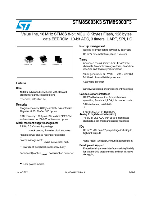
···16-bit generalOC or PWM)with3CAPCO···RAM:memory:128bytes of true data EEPROM;·endurance up to100000write/erase cycles ·Window watchdog and independent watchdog ··I C interface up to400Kbit/s···Flexiblepower crystal resonator oscillator -··Highly robust I/O design,immune against current ·-Low power modes STM8S003K3STM8S003F3Value line,16MHz STM8S8-bit MCU,8Kbytes Flash,128bytes data EEPROM,10-bit ADC,3timers,UART,SPI,I²CInterrupt managementNested interrupt controller with32interrupts·Up to27external interrupts on6vectors LQFP327x7TSSOP20UFQFPN203x3FeaturesCore16MHz advanced STM8core with Harvardarchitecture and3-stage pipeline·Extended instruction setMemoriesProgram memory:8Kbytes Flash;data retention20years at55°C after100cyclesClock,reset and supply management2.95to5.5V operating voltageclock control,4master clock sources:·Power management:(wait,active-halt,halt)-Switch-off peripheral clocks individually·Permanently active,reset consumption power-onTimersAdvanced control timer:16-bit,4CAPCOMchannels,3complementary outputs,dead-timeinsertion and flexible synchronization,·8-bit basic timer with8-bit prescaler·Auto wake-up timerCommunications interfacesUART with clock output for synchronousoperation,Smartcard,IrDA,LIN master mode·SPI interface up to8Mbit/s2Analog to digital converter(ADC)10-bit,±1LSB ADC with up to5multiplexedchannels,scan mode and analog watchdogI/OsUp to28I/Os on a32-pin package including21high sink outputsDevelopment supportEmbedded single wire interface module(SWIM)for fast on-chip programming and non intrusivedebuggingJune2012DocID018576Rev31/100Contents STM8S003K3STM8S003F3 Contents1Introduction (7)2Description (8)3Block diagram (9)4Product overview (10)4.1Central processing unit STM8 (10)4.2Single wire interface module(SWIM)and debug module(DM) (10)4.3Interrupt controller (11)4.4Flash program memory and data EEPROM (11)4.5Clock controller (12)4.6Power management (13)4.7Watchdog timers (13)4.8Auto wakeup counter (14)4.9Beeper (14)4.10TIM1-16-bit advanced control timer (14)4.11TIM2-16-bit general purpose timer (15)4.12TIM4-8-bit basic timer (15)4.13Analog-to-digital converter(ADC1) (15)4.14Communication interfaces (16)4.14.1UART1 (16)4.14.2SPI (17)4.14.3I²C (17)5Pinout and pin description (18)5.1STM8S003K3LQFP32pinout and pin description (18)5.2STM8S003F3TSSOP20/UFQFPN20pinout and pin description (21)5.2.1STM8S003F3TSSOP20pinout and pin description (21)5.2.2STM8S003F3UFQFPN20pinout (22)5.2.3STM8S003F3TSSOP20/UFQFPN20pin description (22)5.3Alternate function remapping (24)6Memory and register map (25)6.1Memory map (25)6.2Register map (26)6.2.1I/O port hardware register map (26)6.2.2General hardware register map (27)6.2.3CPU/SWIM/debug module/interrupt controller registers (36)7Interrupt vector mapping (39)8Option bytes (41)8.1Alternate function remapping bits (43)2/100DocID018576Rev39.3.9 I C interface characteristics (80)STM8S003K3 STM8S003F3Contents9 Electrical characteristics .....................................................................................469.1 Parameter conditions ..................................................................................................46 9.1.1 Minimum and maximum values .......................................................... 46 9.1.2 Typical values ...................................................................................... 46 9.1.3 Typical curves ..................................................................................... 46 9.1.4 Loading capacitor ................................................................................ 46 9.1.5 Pin input voltage ..................................................................................46 9.2 Absolute maximum ratings ......................................................................................... 47 9.3 Operating conditions ...................................................................................................49 9.3.1 VCAP external capacitor ..................................................................... 50 9.3.2 Supply current characteristics ............................................................. 51 9.3.3 External clock sources and timing characteristics .............................. 60 9.3.4 Internal clock sources and timing characteristics ................................ 62 9.3.5 Memory characteristics .. (64)9.3.6 I/O port pin characteristics .................................................................. 66 9.3.7 Reset pin characteristics ..................................................................... 74 9.3.8 SPI serial peripheral interface ............................................................. 77 29.3.10 10-bit ADC characteristics .................................................................819.3.11 EMC characteristics (85)10 Package information ..........................................................................................8910.1 32-pin LQFP package mechanical data ................................................................... 89 10.2 20-pin TSSOP package mechanical data ................................................................. 90 10.3 20-lead UFQFPN package mechanical data ............................................................9211 Thermal characteristics ......................................................................................9411.1 Reference document ................................................................................................ 94 11.2 Selecting the product temperature range .................................................................9412 Ordering information .......................................................................................... 96 13 STM8 development tools ...................................................................................9713.1 Emulation and in-circuit debugging tools .................................................................. 97 13.2 Software tools ...........................................................................................................97 13.2.1 STM8 toolset ..................................................................................... 98 13.2.2 C and assembly toolchains ...............................................................98 13.3 Programming tools ...................................................................................................9814 Revision history ..................................................................................................99DocID018576 Rev 33/100Table 43. I C characteristics (80)List of tablesSTM8S003K3 STM8S003F3List of tablesT able 1. STM8S003xx value line features ............................................................................................... 8 T able 2. Peripheral clock gating bit assignments in CLK_PCKENR1/2 registers ................................. 13 T able 3. TIM timer features ................................................................................................................... 15 T able 4. Legend/abbreviations for pinout tables.................................................................................. 18 T able 5. LQFP32 pin description ........................................................................................................... 19 T able 6. STM8S003F3 pin description .................................................................................................. 22 T able 7. I/O port hardware register map ............................................................................................... 26 T able 8. General hardware register map.............................................................................................. 27 T able 9. CPU/SWIM/debug module/interrupt controller registers........................................................ 36 T able 10. Interrupt mapping .................................................................................................................. 39 T able 11. Option bytes.......................................................................................................................... 99 T able 12. Option byte description .......................................................................................................... 41 T able 13. STM8S003K3 alternate function remapping bits for 32-pin devices ..................................... 43 T able 14. STM8S003F3 alternate function remapping bits for 20-pin devices ..................................... 44 T able 15. Voltage characteristics .......................................................................................................... 47 T able 16. Current characteristics .......................................................................................................... 47 T able 17. Thermal characteristics ......................................................................................................... 48 T able 18. General operating conditions ................................................................................................ 49 T able 19. Operating conditions at power-up/power-down ..................................................................... 50 T able 20. T otal current consumption with code execution in run mode at V DD = 5 V ............................ 51 T able 21. T otal current consumption with code execution in run mode at V DD = 3.3 V ......................... 52 T able 22. T otal current consumption in wait mode at V DD = 5 V ........................................................... 53 T able 23. T otal current consumption in wait mode at V DD = 3.3 V ........................................................ 53 T able 24. T otal current consumption in active halt mode at V DD = 5 V ................................................. 54 T able 25. T otal current consumption in active halt mode at V DD = 3.3 V .............................................. 54 T able 26. T otal current consumption in halt mode at V DD = 5 V ............................................................ 55 T able 27. T otal current consumption in halt mode at V DD = 3.3 V ......................................................... 55 T able 28. Wakeup times ........................................................................................................................ 56 T able 29. T otal current consumption and timing in forced reset state ................................................... 57 T able 30. Peripheral current consumption ............................................................................................ 57 T able 31. HSE user external clock characteristics ................................................................................ 60 T able 32. HSE oscillator characteristics ................................................................................................ 61 T able 33. HSI oscillator characteristics ................................................................................................. 62 T able 34. LSI oscillator characteristics .................................................................................................. 64 T able 35. RAM and hardware registers ................................................................................................. 64 T able 36. Flash program memory and data EEPROM .......................................................................... 65 T able 37. I/O static characteristics ........................................................................................................ 66 T able 38. Output driving current (standard ports) ................................................................................. 68 T able 39. Output driving current (true open drain ports) ....................................................................... 68 T able 40. Output driving current (high sink ports) ................................................................................. 69 T able 41. NRST pin characteristics ....................................................................................................... 74 T able 42. SPI characteristics .................................................................................................................78 2 T able 44. ADC characteristics ............................................................................................................... 82 T able 45. ADC accuracy with R AIN < 10 kΩ , V DD = 5 V........................................................................ 82 T able 46. ADC accuracy with R AIN < 10 kΩ R AIN , V DD = 3.3 V............................................................. 83 T able 47. EMS data ...............................................................................................................................864/100DocID018576 Rev 3STM8S003K3STM8S003F3List of tablesT able48.EMI data (86)T able49.ESD absolute maximum ratings (87)T able50.Electrical sensitivities (88)T able51.32-pin low profile quad flat package mechanical data (89)T able52.20-pin,4.40mm body,0.65mm pitch mechanical data (91)T able53.20-lead ultra thin fine pitch quad flat no-lead package(3x3)mechanical data (92)T able54.Thermal characteristics (94)T able55.Document revision history (99)DocID018576Rev35/100Figure 41. Typical application with I C bus and timing diagram (84)List of figuresSTM8S003K3 STM8S003F3List of figuresFigure 1. Block diagram .......................................................................................................................... 9 Figure 2. Flash memory organization ................................................................................................... 12 Figure 3. STM8S003K3 LQFP32 pinout ............................................................................................... 18 Figure 4. STM8S003F3 TSSOP20 pinout ............................................................................................. 21 Figure 5. STM8S003F3 UFQFPN20-pin pinout .................................................................................... 22 Figure 6. Memory map .......................................................................................................................... 25 Figure 7. Pin loading conditions ............................................................................................................ 46 Figure 8. Pin input voltage .................................................................................................................... 47 Figure 9. f CPUmax versus V DD ............................................................................................................... 50 Figure 10. External capacitor C EXT ...................................................................................................... 50 Figure 11. Typ I DD(RUN) vs. V DD HSE user external clock, f CPU = 16 MHz ............................................ 58 Figure 12. Typ I DD(RUN) vs. f CPU HSE user external clock, V DD = 5 V ................................................... 58 Figure 13. Typ I DD(RUN) vs. V DD HSI RC osc, f CPU = 16 MHz ................................................................ 59 Figure 14. Typ I DD(WFI) vs. V DD HSE user external clock, f CPU = 16 MHz ............................................. 59 Figure 15. Typ I DD(WFI) vs. f CPU HSE user external clock, V DD = 5 V .................................................... 60 Figure 16. Typ I DD(WFI) vs. V DD HSI RC osc, f CPU = 16 MHz ................................................................ 60 Figure 17. HSE external clock source ................................................................................................... 61 Figure 18. HSE oscillator circuit diagram .............................................................................................. 62 Figure 19. Typical HSI frequency variation vs V DD @ 4 temperatures ................................................. 63 Figure 20. Typical LSI frequency variation vs V DD @ 4 temperatures .................................................. 64 Figure 21. Typical V IL and V IH vs V DD @ 4 temperatures ..................................................................... 67 Figure 22. Typical pull-up resistance vs V DD @ 4 temperatures ........................................................... 67 Figure 23. Typical pull-up current vs V DD @ 4 temperatures ................................................................ 68 Figure 24. Typ. V OL @ V DD = 5 V (standard ports) ............................................................................... 70 Figure 25. Typ. V OL @ V DD = 3.3 V (standard ports) ............................................................................ 70 Figure 26. Typ. V OL @ V DD = 5 V (true open drain ports) ..................................................................... 71 Figure 27. Typ. V OL @ V DD = 3.3 V (true open drain ports) .................................................................. 71 Figure 28. Typ. V OL @ V DD = 5 V (high sink ports) ............................................................................... 72 Figure 29. Typ. V OL @ V DD = 3.3 V (high sink ports) ............................................................................ 72 Figure 30. Typ. V DD - V OH @ V DD = 5 V (standard ports) ...................................................................... 73 Figure 31. Typ. V DD - V OH @ V DD = 3.3 V (standard ports) .................................................................. 73 Figure 32. Typ. V DD - V OH @ V DD = 5 V (high sink ports) ...................................................................... 74 Figure 33. Typ. V DD - V OH @ V DD = 3.3 V (high sink ports) ................................................................... 74 Figure 34. Typical NRST V IL and V IH vs V DD @ 4 temperatures .......................................................... 76 Figure 35. Typical NRST pull-up resistance vs V DD @ 4 temperatures ................................................ 76 Figure 36. Typical NRST pull-up current vs V DD @ 4 temperatures ..................................................... 77 Figure 37. Recommended reset pin protection ..................................................................................... 77 Figure 38. SPI timing diagram - slave mode and CPHA = 0 ................................................................. 79 Figure 39. SPI timing diagram - slave mode and CPHA = 1 ................................................................. 79 Figure 40. SPI timing diagram - master mode (1) ..................................................................................80 2 Figure 42. ADC accuracy characteristics .............................................................................................. 84 Figure 43. Typical application with ADC ............................................................................................... 85 Figure 44. 32-pin low profile quad flat package (7 x 7) ......................................................................... 89 Figure 45. 20-pin, 4.40 mm body, 0.65 mm pitch .................................................................................. 90 Figure 46. 20-lead ultra thin fine pitch quad flat no-lead package outline (3x3) ................................... 92 Figure 47. STM8S003x value line ordering information scheme ..........................................................966/100DocID018576 Rev 3· · For informationto the STM8S Flash programming manual (PM0051).internal Flash memory· For information on the protocol and debug module user manual (UM0470). to the STM8· For information on the STM8 core, please refer to the STM8 CPU programming manualSTM8S003K3 STM8S003F3Introduction1IntroductionThis datasheet contains the description of the device features, pinout, electrical characteristics, mechanical data and ordering information.For complete information on the STM8S microcontroller memory, registers and peripherals, please refer to the STM8S microcontroller family reference manual (RM0016).on programming, erasing and protection of the please referdebug and SWIM (single wire interface module) refer SWIM communication(PM0044).DocID018576 Rev 37/100Multipurpose timer (TIM1), SPI, I C, UARTDescription2STM8S003K3 STM8S003F3DescriptionThe STM8S003x value line 8-bit microcontrollers feature 8 Kbytes Flash program memory, plus integrated true data EEPROM. The STM8S microcontroller family reference manual (RM0016) refers to devices in this family as low-density. They provide the following benefits: performance, robustness, and reduced system cost.Device performance and robustness are ensured by integrated true data EEPROM supporting up to 100000 write/erase cycles, advanced core and peripherals made in a state-of-the art technology, a 16 MHz clock frequency, robust I/Os, independent watchdogs with separate clock source, and a clock security system.The system cost is reduced thanks to high system integration level with internal clock oscillators, watchdog and brown-out reset.Full documentation is offered as well as a wide choice of development tools.Table 1: STM8S003xx value line featuresDevice Pin countMaximum number of GPIOs (I/Os) Ext. interrupt pins Timer CAPCOM channels Timer complementary outputs A/D converter channels High sink I/OsSTM8S003K3 32 28 27 7 3 4 21STM8S003F3 20 16 16 7 2 5 12 Low density Flash program memory (bytes) 8K 8K RAM (bytes)True data EEPROM (bytes) 1K 128 (1)1K 128 (1)2Peripheral setwindow WDG,independent WDG, ADC, PWM timer (TIM2), 8-bit timer (TIM4)(1) Without read-while-write capability.8/100DocID018576 Rev 3A d d r e s s a n d d a t a b u sSTM8S003K3 STM8S003F3Block diagram3Block diagramFigure 1: Block diagramReset blockClock controllerXTAL 1-16 MHzResetSingle wire debug interf.400 Kbit/s8 Mbit/sResetPORBORSTM8 coreDebug/SWIMI2CSPIDetectorClock to peripherals and coreRC int. 16 MHzRC int. 128 kHzWindow WDGIndependent WDG8-Kbyte program Flash 128-bytedata EEPROM1-KbyteRAMUp to4 CAPCOM channels +3LIN master SPI emul.UART116-bit advanced control timer (TIM1)16-bit general purposetimer (TIM2)complementaryoutputsUp to3 CAPCOMchannels8-bit basic timerUp to 5 channels1/2/4 kHzbeepADC1BeeperDocID018576 Rev 3(TIM4)AWU timer9/100· · Xand read-modify-write type data manipulations addressing modes with or without offset · · Indexed indirect addressing mode for look-up tables located anywhere in the address ·Product overviewSTM8S003K3 STM8S003F344.14.210/100Product overviewThe following section intends to give an overview of the basic features of the device functional modules and peripherals.For more detailed information please refer to the corresponding family reference manual (RM0016).Central processing unit STM8The 8-bit STM8 core is designed for code efficiency and performance.It contains 6 internal registers which are directly addressable in each execution context, 20 addressing modes including indexed indirect and relative addressing and 80 instructions.Architecture and registers Harvard architecture· 3-stage pipeline · 32-bit wide program memory bus - single cycle fetching for most instructionsand Y 16-bit index registers - enabling indexed · 8-bit accumulator · 24-bit program counter - 16-Mbyte linear memory space · 16-bit stack pointer - access to a 64 K-level stack · 8-bit condition code register - 7 condition flags for the result of the last instructionAddressing20 addressing modesspace · Stack pointer relative addressing mode for local variables and parameter passingInstruction set80 instructions with 2-byte average instruction size· Standard data movement and logic/arithmetic functions · 8-bit by 8-bit multiplication · 16-bit by 8-bit and 16-bit by 16-bit division · Bit manipulation · Data transfer between stack and accumulator (push/pop) with direct stack access · Data transfer using the X and Y registers or direct memory-to-memory transfersSingle wire interface module (SWIM) and debug module (DM)The single wire interface module and debug module permits non-intrusive, real-time in-circuit debugging and fast memory programming.DocID018576 Rev 3· · 128 bytes ofbyte area EEPROM· ·STM8S003K3 STM8S003F3Product overviewSWIMSingle wire interface module for direct access to the debug module and memory programming. The interface can be activated in all device operation modes. The maximum data transmission speed is 145 bytes/ms. Debug moduleThe non-intrusive debugging module features a performance close to a full-featured emulator. Beside memory and peripherals, also CPU operation can be monitored in real-time by means of shadow registers.R/W to RAM and peripheral registers in real-time· R/W access to all resources by stalling the CPU · Breakpoints on all program-memory instructions (software breakpoints) · Two advanced breakpoints, 23 predefined configurations4.34.4Interrupt controller· Nested interrupts with three software priority levels · 32 interrupt vectors with hardware priority · Up to 27 external interrupts on 6 vectors including TLI · Trap and reset interruptsFlash program memory and data EEPROM· 8 Kbytes of Flash program single voltage Flash memorytrue data User optionWrite protection (WP)Write protection of Flash program memory and data EEPROM is provided to avoid unintentional overwriting of memory that could result from a user software malfunction.There are two levels of write protection. The first level is known as MASS (memory access security system). MASS is always enabled and protects the main Flash program memory, the data EEPROM, and the option bytes.T o perform in-application programming (IAP), this write protection can be removed by writing a MASS key sequence in a control register. This allows the application to modify the content of the main program memory and data EEPROM, or to reprogram the device option bytes. A second level of write protection, can be enabled to further protect a specific area of memory known as UBC (user boot code). Refer to the figure below.The size of the UBC is programmable through the UBC option byte, in increments of 1 page (64-byte block) by programming the UBC option byte in ICP mode. This divides the program memory into two areas: Main program memory: 8 Kbytes minus UBC· User-specific boot code (UBC): Configurable up to 8 KbytesThe UBC area remains write-protected during in-application programming. This means that the MASS keys do not unlock the UBC area. It protects the memory used to store the bootDocID018576 Rev 311/100。
SM-01-E 输入输出接口定义

SM-01-E 输入输出接口定义SM-01-E输入输出接口定义:★JP1, JP2, JP3 为外部开关信号输入口,公共端为JP3-7、8JP1.01: 输入X0,检修信号,断开为检修,闭合为自动JP1.02: 输入X1,上行信号. 在检修时闭合为点动上行,在司机时闭合为上行换向JP1.03: 输入X2,下行信号. 在检修时闭合为点动下行,在司机时闭合为下行换向JP1.04: 输入X3,上行多层终端换速开关, 2 米/秒以上电梯要求使用, (低速电梯不用此信号时,请设置输入类型X3 为常开)JP1.05: 输入X4,下行多层终端换速开关, 2 米/秒以上电梯要求使用, (低速电梯不用此信号时,请设置输入类型X4 为常开)JP1.06: 输入X5,上行限位开关JP1.07: 输入X6,上行限位开关JP1.08: 输入X7,上行单层终端换速开关.JP3.09: 输入X8,下行单层终端换速开关.JP1.10: 输入X9,上平层干簧JP2.1: 输入X10,下平层干簧JP2.2: 输入X11,调速器故障输出信号JP2.3: 输入X12,消防开关JP2.4: 输入X13,安全回路继电器检测JP2.5: 输入X14,门锁回路继电器检测JP2.6: 输入X15,调速器进线接触器检测JP2.7: 输入X16,调速器出线接触器检测JP2.8: 输入X17,抱闸继电器检测JP2.9: 输入X18,门区信号输入,用于开门再平层和提前开门,闭合有效JP2.10: 输入X19,调速器运行信号检测,检测到此信号闭合则抱闸可以张开JP3.01: 输入X20,提前开门继电器检测JP3.02: 输入X21,备用JP3.03: 输入X22,抱闸开关JP3.04: 输入X23,备用JP3.05: 输入X24,备用JP3.06: 输入X25,备用JP3.07: X0-X25 输入信号公共端JP3.08: X0-X25 输入信号电源端JP3.09: X0-X25 输入信号公共端,0V.JP3.10: X0-X25 输入信号电源端,+24V.★输入信号常开点/常闭点设置的意义是:如果此信号没有动作,输出信号是导通的,则称此信号为常闭信号。
- 1、下载文档前请自行甄别文档内容的完整性,平台不提供额外的编辑、内容补充、找答案等附加服务。
- 2、"仅部分预览"的文档,不可在线预览部分如存在完整性等问题,可反馈申请退款(可完整预览的文档不适用该条件!)。
- 3、如文档侵犯您的权益,请联系客服反馈,我们会尽快为您处理(人工客服工作时间:9:00-18:30)。
SM-01/02/04端口定义说明
SM-01板
1. 主控制器SM-01-B 输入输出接口定义
★ JP3.01 - JP4.06 为外部开关信号输入口,
JP4.7 和JP4.8 需要外部+24V 电源输入,作为外部输入信号的隔离电源
表 2.1
※TE-MRL、TE-GL及TE-E型控制柜,对于SM-01板的软件版本在3C021227以下(不含3C021227)JP5的端口定义变化如下:
2.其它接口的定义说明:
JP1: JTAG 编程接口,支持在线编程
JP2: LCD 人机界面接口
DB1: RS232/RS485 MODEM 远程监控接口。
DB1.1: DCD DB1.2: RXD
DB1.3: TXD DB1.4: DTR
DB1.5: SGND DB1.6: RS485-A
DB1.7: RS485-B DB1.8: X
DB1.9: X
3. 跳线的配置说明:
J1:并联口终端电阻,总是短接J2: 编码器电源电压选择,
J2短接1-2,控制器提供15V/40mA电源到端口JP6.02(仅在调速器不能提供编码器电源的情况下,才由
控制器给编码器供电)
J2短接2-3,控制器提供5V/100mA电源到端口JP6.02(仅在调速器不能提供编码器电源的情况下,才由
控制器给编码器供电)
J3,J4: 编码器类型选择
J3和J4同时短接1-2,控制器使用JP6.03,JP6.04输入的OC或推挽输出编码器信号。
J3和J4同时短接2-3,控制器使用JP6.05,JP6.06,JP6.07,JP6.08输入的差分编码器信号。
J5: RS232/RS485 选择,
短接<J5.2-J5.3>,通讯方式为RS232,可以配置MODEM 和电话线,进行远程监控。
短接<J5.1-J5.2>,通讯方式为RS485,进行集中监控。
SM-02板
1. 轿厢控制器(SM-02-B)的接口定义
JP6:四芯通讯线
JP6.01: TXV+ JP6.02: TXV-
JP6.03: TXA+ JP6.04: TXA-
JP5: 输入端
JP5.01: 输入TX0-TX18 信号公共端,0V. JP5.02: 输入TX0, 前门开门到位
JP5.03: 输入TX1, 前门关门到位JP5.04: 输入TX2, 前门安全触板
JP5.05: 输入TX3, 超载( >= 110% ) JP5.06: 输入TX4, 满员( >= 100% ) JP5.07: 输入TX5, 重载( >= 65% ) JP5.08: 输入TX6, 轻载( >= 35% )
JP5.09: 输入TX7, 空载( <= 10% ) JP5.10: 输入TX8, 司机
JP5.11: 输入TX9, 专用JP5.12: 输入TX10,司机直驶
JP5.13: 输入TX11, 后门开门到位JP5.14: 输入TX12, 后门关门到位
JP5.15: 输入TX13, 后门安全触板JP5.16: 输入TX14, 备用
JP5.17: 输入TX15, 备用JP5.18: 输入TX16, 备用
JP5.19: 输入TX17, 备用JP5.20: 输入TX18, 备用
JP2: 输出端
JP2.01: 输出TY0, 上到站钟JP2.02: 输出TY0, 上到站钟
JP2.03: 输出TY1, 下到站钟JP2.04: 输出TY1, 下到站钟
JP2.05: 输出TY2, 轿厢照明JP2.06: 输出TY2, 轿厢照明
★JP2.05,JP2.06 断开时,轿厢照明打开JP2.05,JP2.06 闭合时,轿厢照明关闭
JP2.07: 输出TY3, 备用JP2.08: 输出TY3, 备用
★JP2.01-JP2.08共8个点为继电器触点输出
JP2.09: 输出TY4, 超载灯- JP2.10: 输出TY4, 超载灯+
JP2.11: 输出TY5, 蜂鸣器- JP2.12: 输出TY5, 蜂鸣器+
JP2.13: 输入模拟量负载信号+ JP2.14: 输入模拟量负载信号- (模拟量负载信号为0-5V 信号,满载时调整到4V,空载为0V)
JP2.15: RS485+ JP2.16: RS485-
(RS485+,RS485-为通讯口,预定义为语音接口)
JP2.17: 备用JP2.18: 备用
JP2.19: 隔离电源输入+ JP2.20: 隔离电源输入-
JP3:
JP3.1: 开门指示灯- JP3.2: 开门指示灯+
JP3.3: 开门按键JP3.4: 开门按键TX19
按钮,使显示“0”时拿掉短接针。
4.有关外呼显示设置
当SM-04作为外呼显示板时,应正确设置楼层,将跳线短接S1,按实际楼层数,即从最底层从“1”
开始,逐层设置,设置完拿掉S1。
5.有关锁梯的设置
如果此层楼作为锁梯层,则在此层楼的外呼板的跳线短接S2,并且不要拔下。