comsol培训的仿真实例
comsol电磁场仿真案例科学工...
comsol电磁场仿真案例科学工程计算与应用——基于COMSOL数值模拟的工业应用案例(伍仞之)_图文导读:就爱阅读网友为您分享以下“科学工程计算与应用——基于COMSOL数值模拟的工业应用案例(伍仞之)_图文”的资讯,希望对您有所帮助,感谢您对的支持! 试井分析随钻电磁波传播测井-卧式刻度装置随钻电磁波传播测井-卧式刻度装置专题之七——科学工程计算与应用基于COMSOL数值模拟的工业应用案例伍仞之跨学科研究和多物理分析为科技创新带来了新契机1、物理问题的发现和解决方法,一直和数学密切相关,物理学的发展深深依赖于数学理论的发展。
2、依据物理学原理归纳出来的偏微分方程,统称为数学物理方程(包括具有物理意义的积分方程、微分积分方程和常微分方程)。
3、数学方法的发展正在改变着我们认识世界的方式!COMSOL Multiphysics应用领域电磁场工程-微电机系统;微波工程;无线电频率部件;脉冲涡流应力检测;微波化学;微波加热;永磁体;声学应用工程-声波传播;建筑声学;汽车消音器;超声无损检测;化学工程-化学反应;燃料电池;电化学;传递现象;反应工程;生物化学;动力工程-空气动力学;流体动力学;多孔介质渗流;结构力学;弹性力学;热工程-地球科学;热传导;弥散;热处理;物理学-光学;光子学;量子力学;半导体设备;材料科学-复合材料;电磁学;理论力学;理论声学;热学;多物理场耦合-电、热耦合;流、固耦合;压电压磁材料与固体力学耦合;磁、声耦合;Darcy -Brinkman -Navier-Stokes 渗流;COMSOL Multiphysics应用领域军事工程-潜艇;飞机;战舰消磁;电磁动力;电磁炮;生物医学工程-生物科学;医学声波检测;核磁共振;磁声成像;生物力学;生物电磁;地球科学-电磁勘探;测井;油藏工程;钻井工程;三次采油;水文、环境工程、岩土工程、矿业工程、地球物理;传递过程-动量传递;热量传递;质量传递;广义通用控制方程;非稳定项+对流项=扩散项+源项(?u?)???(????)?S???(?uj?)?( )?S?,j?1,2,3?x,y,z?t?t?xj?xj?xj科学计算-数值模拟技术(FEA);偏微分方程数值计算;交叉学科-机械、电子、流体、传热、光学及电磁学等其它-MEMS器件、纳米材料、纳米粉体、介孔材料、纳米管/纤维、…COMSOL Multiphysics应用领域1、人类科学研究的三种方法? 理论方法? 室内实验方法? 数值实验方法2、地球物理测井方法理论研究理论上研究的各种地球物理测井法问题,地质问题解释模拟地层测井响应数值实验归纳测井物理问题确定测井数学模型完全可以等价于研究偏微分方程的边值数学求解问题3、应用数学工作者如何尽快走进地球物理测井领域COMSOL —应用模块COMSOL—自定义模块和应用模式多物理场的图标声学化学反应和多组分传递电磁波传播基于公式建模流动传热准静态和静态电磁结构力学系统和电路建模Comsol-模块功能Comsol-模块功能Comsol-操作界面Comsol-有限元数值模拟Comsol-数值模拟问题分析流程AC/DC模块。
Comsol经典实例017:双绕组圆环天线的无线电能传输仿真
在 COMSOL Multiphysics 5.5 版本中创建Comsol经典实例017:双绕组圆环天线的无线电能传输仿真无线电能传输是指发射单元和接收单元之间的无接触式能量传输,为电气设备提供了一种简便的充电方法,并支持同时对多个设备进行充电。
随着技术的持续发展,无线充电的应用日趋广泛,涵盖手机、日用品、新能源汽车等。
在本案例中,系统全面地介绍如何使用 COMSOL Multiphysics® 对无线充电设备进行多物理场耦合建模仿真,包括:线圈建模、天线激励的设置、天线之间的能量耦合、位置更改对能量传输效率的影响等。
同时,还将结合案例讲解建模设置的要点及注意事项,并演示在 COMSOL® 5.5 中如何对无线充电设备进行仿真。
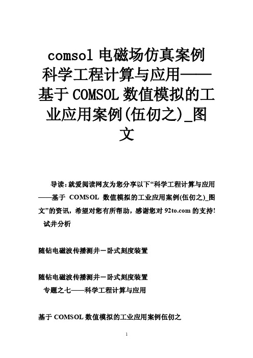
一、案例简介本例通过研究针对 UHF RFID 频率调谐的两个圆环天线之间的能量耦合,阐述了无线电能传输的概念,并通过片式电感器来减小天线的尺寸。
发射天线的方向固定,而接收天线旋转,我们根据S参数研究最佳耦合构型。
图1 基于接收天线方向计算两个圆环天线之间耦合效应的模型。
空气域和完美匹配层未在此图中显示二、模型定义模型由两个印刷圆环天线组成,天线被带有完美匹配层(PML) 的空气域包围。
对于UFH RFID 通信,天线的工作频率为915 MHz。
薄铜层在2 mm 聚四氟乙烯 (PTFE) 板上形成图案。
铜层的厚度从几何上看非常薄,但它比该频率下铜的集肤深度s =2.15 μm 厚得多,因此将其模拟为理想电导体(PEC)。
通过在每个圆形铜迹线的中间插入代表0805 表面贴装器件的集总电感器,使天线直径减小到约0.22λ0。
在配置为PEC 的每条迹线的分离部分,分配一个具有50 Ω参考阻抗的集总端口来激励或终止天线。
周围需要有完美匹配层才能吸收发射天线的辐射并描述无限自由空间中的天线耦合。
三、结果与讨论图2 显示xy 平面上的电场模分布,以及发射天线的功率流随接收天线旋转角度变化的箭头图。
comsol单模光纤仿真案例
comsol单模光纤仿真案例Step-Index FiberIntroductionThe transmission speed of optical waveguides is superior to microwave waveguides because optical devices have a much higher operating frequency than microwaves, enabling a far higher bandwidth.Today the silica glass (SiO 2) fiber is forming the backbone of modern communication systems. Before 1970, optical fibers suffered from large transmission losses, making optical communication technology merely an academic issue. In 1970, researchers showed, for the first time, that low-loss optical fibers really could be manufactured. Earlier losses of 2000 dB/km now went down to 20 dB/km. Today’s fibers have losses near the theoretical limit of 0.16 dB/km at 1.55 μm (infrared light).One of the winning devices has been the single-mode fiber, having a step-index profile with a higher refractive index in the center core and a lower index in the outer cladding. Numerical software plays an important role in the design of single-mode waveguides and fibers. For a fiber cross section, even the most simple shape is difficult and cumbersome to deal with analytically.A circular step-index waveguide is a basic shape where benchmark results are available (see Ref. 1).This example is a model of a single step-index waveguide made of silica glass. The inner core is made of pure silica glass with refractive index n 1 = 1.4457 and the cladding is doped, with a refractive index of n 2 = 1.4378. These values are valid for free-space wavelengths of 1.55 μm. The radius of the cladding is chosen to be large enough so that the field of confined modes iszero at the exterior boundaries.For a confined mode there is no energy flow in the radial direction, thus the wave must be evanescent in the radial direction in the cladding. This is true only ifOn the other hand, the wave cannot be radially evanescent in the core region. ThusThe waves are more confined when n eff is close to the upper limit in this interval.n eff n 2>n 2n eff n 1<<Model DefinitionThe mode analysis is made on a cross-section in the xy -plane of the fiber. The wave propagates in the z direction and has the formwhere ω is the angular frequency and β the propagation constant. An eigenvalue equation for the electric field E is derived from Helmholtz equationwhich is solved for the eigenvalue λ = ?j β.As boundary condition along the outside of the cladding the electric field is set to zero. Because the amplitude of the field decays rapidly as a function of the radius of the cladding this is a valid boundary condition.Results and DiscussionWhen studying the characteristics of optical waveguides, the effective mode index of a confined mode,as a function of the frequency is an important characteristic.A common notion is the normalized frequency for a fiber. This is defined aswhere a is the radius of the core of the fiber. For this simulation, the effective mode index for the fundamental mode,1.4444 corresponds to a normalized frequency of4.895. The electric and magnetic fields for this mode is shown in Figure 1 below.E x y z t ,,,()E x y ,()e j ωt βz –()=??E ×()×k 02n 2E –0=n eff βk 0-----=V 2πa λ0----------n 12n 22–k 0a n 12n 22–==Figure 1: The surface plot visualizes the z component of the electric field. This plot is for the effective mode index 1.4444.Reference1. A. Yariv, Optical Electronics in Modern Communications, 5th ed., Oxford University Press, 1997.Model Library path:RF_Module/Tutorial_Models/step_index_fiberModeling InstructionsFrom the File menu, choose New.N E W1In the New window, click Model Wizard.M O D E L W I Z A R D1In the Model Wizard window, click 2D.2In the Select physics tree, select Radio Frequency>Electromagnetic Waves, Frequency Domain (emw).3Click Add.4Click Study.5In the Select study tree, select Preset Studies>Mode Analysis.6Click Done.G E O M E T R Y11In the Model Builder window, under Component 1 (comp1) click Geometry 1.2In the Settings window for Geometry, locate the Units section.3From the Length unit list, choose μm.Circle 1 (c1)1On the Geometry toolbar, click Primitives and choose Circle.2In the Settings window for Circle, locate the Size and Shape section.3In the Radius text field, type 40.4Click the Build Selected button.Circle 2 (c2)1On the Geometry toolbar, click Primitives and choose Circle.2In the Settings window for Circle, locate the Size and Shape section.3In the Radius text field, type 8.4Click the Build Selected button.M A T E R I A L SMaterial 1 (mat1)1In the Model Builder window, under Component 1 (comp1) right-click Materials and choose Blank Material.2Right-click Material 1 (mat1) and choose Rename.3In the Rename Material dialog box, type Doped Silica Glass in the New label text field.4Click OK.5Select Domain 2 only.6In the Settings window for Material, click to expand the Material properties section. 7Locate the Material Properties section. In the Material properties tree, select Electromagnetic Models>Refractive Index>Refractive index (n).8Click Add to Material.9Locate the Material Contents section. In the table, enter the following settings:Property Name Value Unit Property groupRefractive index n 1.44571Refractive indexMaterial 2 (mat2)1In the Model Builder window, right-click Materials and choose Blank Material.2Right-click Material 2 (mat2) and choose Rename.3In the Rename Material dialog box, type Silica Glass in the New label text field. 4Click OK.5Select Domain 1 only.6In the Settings window for Material, click to expand the Material properties section. 7Locate the Material Properties section. In the Material properties tree, select ElectromagneticModels>Refractive Index>Refractive index (n).8Click Add to Material.9Locate the Material Contents section. In the table, enter the following settings:Property Name Value Unit Property groupRefractive index n 1.43781Refractive indexE L E C T R O M A G N E T I C W A V E S,F R E Q U E N C Y D O M A I N(E M W)Wave Equation, Electric 11In the Model Builder window, expand the Component 1 (comp1)>Electromagnetic Waves, Frequency Domain (emw) node, then click Wave Equation, Electric 1.2In the Settings window for Wave Equation, Electric, locate the Electric Displacement Field section.3From the Electric displacement field model list, choose Refractive index.M E S H11In the Model Builder window, under Component 1 (comp1) click Mesh 1.2In the Settings window for Mesh, locate the Mesh Settings section.3From the Element size list, choose Finer.4Click the Build All button.S T U D Y1Step 1: Mode Analysis1In the Model Builder window, under Study 1 click Step 1: Mode Analysis.2In the Settings window for Mode Analysis, locate the Study Settings section.3In the Search for modes around text field, type 1.446. Themodes of interest have an effective mode index somewhere between the refractive indices of the two materials. The fundamental mode has the highest index. Therefore, setting the mode index to search around to something just above the core index guarantees that the solver will find the fundamental mode.4In the Mode analysis frequency text field, type c_const/1.55[um]. This frequency corresponds to a free space wavelength of 1.55 μm.5On the Model toolbar, click Compute.R E S U L T SElectric Field (emw)1Click the Zoom Extents button on the Graphics toolbar.2Click the Zoom In button on the Graphics toolbar.3The default plot shows the distribution of the norm of the electric field for the highest of the 6 computed modes (the one with the lowest effective mode index).To study the fundamental mode, choose the highest mode index. Because the magnetic field is exactly 90 degrees out of phase with the electric field you can see both the magnetic and the electric field distributions by plotting the solution at a phase angle of 45 degrees.Data Sets1In the Model Builder window, expand the Results>Data Sets node, then click Study 1/ Solution 1.2In the Settings window for Solution, locate the Solution section.3In the Solution at angle (phase) text field, type 45.Electric Field (emw)1In the Model Builder window, under Results click Electric Field (emw).2In the Settings window for 2D Plot Group, locate the Data section.3From the Effective mode index list, choose 1.4444 (2).4In the Model Builder window, expand the Electric Field (emw) node, then click Surface 1.5In the Settings window for Surface, click Replace Expression in the upper-right corner of the Expression section. From the menu, choose Model>Component1>Electromagnetic Waves, Frequency Domain>Electric>Electric field>emw.Ez - Electricfield, z component.6On the 2D plot group toolbar, click Plot.Add a contour plot of the H-field.7In the Model Builder window, right-click Electric Field (emw) and choose Contour.8In the Settings window for Contour, click Replace Expressionin the upper-right corner of the Expression section. From the menu, choose Model>Component1>Electromagnetic Waves, Frequency Domain>Magnetic>Magnetic field>emw.Hz -Magnetic field, z component.9On the 2D plot group toolbar, click Plot. The distribution of the transversal E and H field components confirms that this is the HE11 mode. Compare the resulting plot with that in Figure 1.。
基于comsol的仿真实验
一、实验目的熟悉掌握COMSOL Multiphysics软件,通过3D有限元建模方法,建立铂电极-玻璃体-视网膜的分层电刺激模型。
深入研究电极如何影响电刺激效果,系统的分析了电极尺寸、电极到视网膜表面的距离等参数对视网膜电刺激的影响,为视网膜视觉假体刺激电极的刺激效果提供指导意义,进一步优化电刺激效果,达到提高人工视觉的修复效果。
二、实验仪器设备计算机,COMSOL Multiphysics软件三、实验原理影响视网膜电刺激效果的因素有许多:电极尺寸、电极距视网膜距离、电极形状、电极排列等,这里主要从电极尺寸,电极距视网膜距离来探讨。
视网膜电刺激模型通过参考视网膜解剖结构构建,电刺激的有效响应区域取决于神经节细胞层(GCL)电场强度是否大于1000V/m,当大于该值时认为该区域神经节细胞能够兴奋,进而指导电极尺寸、电极距视网膜距离的参数。
四、实验内容根据视网膜的解剖结构来构建相应的视网膜分层模型,模型总共分为8层:玻璃体层,神经节细胞层,内网状层,内核层,外网状层,外核层,视网膜下区域,色素上皮层,脉络膜及巩膜。
根据视网膜各层的导电特性来设定相应的导电率,模型构建,设置边界条件。
在电极处施加相应电流刺激,规定神经节细胞层(GCL)电场强度(>1000V/m)时认为能够引起视神经细胞兴奋,在确定的电流强度下,神经节细胞层(GCL)层电场强度大于1000V/m的区域认为有效响应区域,进而判断电极刺激的有效响应区域,指导电极尺寸r和电极距视网膜距离h等参数设置。
其具体实验步骤如下所示:1、根据视网膜的解剖特性构建视网膜分层模型。
模型在三维模式下电磁场子目录下的传导介质DC场下建立。
进入建模窗口后,在绘图栏下设置模型为圆柱体,输入各部分的长宽高数值,轴基准点为圆柱体的圆心坐标。
模型分为9层(11个求解域),其示图如下:图1 视网膜分层模型2、模型建好后,在菜单栏下的物理量里面选择求解域设定,对示图的11个求解域进行设定传导率,如图2所示,其中每一层的电导率情况参考于视网膜导电特性。
COMSOL3.5快速入门案例1——导电体的热效应
COMSOL Multiphysics快速入门实例: 导电体的热效应导电体的热效应该模型的目的在于给出一个多物理场模型的概念并给出采用COMSOL Multiphysics求解这类问题的方法。
该实例研究了热和电流平衡之间的耦合作用现象。
装置中通有直流电流。
由于装置的有限电导率,在电流流过装置的过程中会出现发热现象,装置的温度将会显著上升,从而也将改变材料的导电率。
这种作用过程是双向耦合的过程;即电流平衡影响到热平衡,而热平衡又反过来影响到电流平衡。
模型的过程包含以下两个基本过程:• 绘制装置的结构图• 定义物理环境,设置材料属性和边界条件• 绘制网格• 选择一个合适的求解器并开始求解过程• 后处理结果COMSOL Multiphysics 包含一个非常易用的CAD工具,在该模型中将会得到介绍。
你可能更习惯于采用其它的CAD工具来绘制几何图形,然后将其导入到COMSOL Multiphysics中; 如果是采用这种方式,则可以跳过下面的几何结构绘制过程介绍,而通过导入一个CAD文件到COMSOL Multiphysics 中来作为分析模型,在安装目录下有为该模型准备的分析CAD几何模型文件。
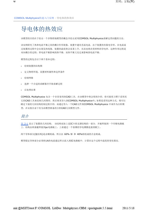
简介图 2-1显示了装置的几何结构, 该结构实际上是IC卡的支撑结构的一部分,并被焊接到一个印刷电路板上。
结构由两条腿焊接到pc电路板上,上部通过一个很薄的导电薄膜连接到IC上。
两个导体部分(腿结构)是由铜制成,焊点由 60% 锑 和 40%铅组成的合金制成.模型假定导体部分必须将1A的电流通过焊点流入到IC电路板中,计算在这个过程中温度的变化情况。
图 2-1: 装置的几何结构模型定义电流平衡条件由下列方程式来描述其中 σmetal 表示电导率(S/m), V 表示电势(V). 电导率是温度相关函数,用下列表达式来描述:其中 ρ0 表示在参考温度T 0 (K)下的参考电阻 (Ω·m), a 表示温度因变量的比例系数 (K -1)。
comsolmultiphysics精典实例直线电机建模仿真

模型描述 – 方程
在二维问题中,COMSOL利用磁势A的静磁方程求解该问题
01r1Az 0 0 1 1 rr 1 1B BrryxJze
结果
Z分量的电势分布
感 谢
COMSOL AC/DC模块培训
主讲人: 上海中仿科技
利用COMSOL计算直线电机
直线电机是一种不用其他装置就能产生直线运动的 电机设备。沿半径方向把旋转电机的定子和转子切开,产 生一个直线推力,就成了直线电机。
AC/DC_Module/Motors_and_Drives/coil_LEM
模型描述 –几何
comsol案例

comsol案例Comsol案例。
最近,我在工程领域中使用了Comsol Multiphysics软件进行了一些仿真分析,我想在这里分享一些我使用Comsol的案例以及一些心得体会。
首先,我想谈谈使用Comsol进行热传导仿真的经验。
在我的项目中,我需要对一个导热材料进行热传导性能的分析。
通过Comsol软件,我能够轻松地建立起材料的热传导模型,并且进行了多种工况下的仿真分析。
我发现Comsol提供了丰富的材料性能库,这使得我能够快速地找到我需要的材料参数,并且在仿真过程中进行调整。
通过Comsol的热传导模块,我成功地得到了材料在不同温度下的热传导性能,这对于我后续的工程设计提供了重要的参考。
其次,我还使用Comsol进行了电磁场仿真。
在我的项目中,我需要对一个电磁场传感器进行性能分析。
通过Comsol的电磁场模块,我能够建立起传感器的电磁场模型,并且进行了多种工况下的仿真分析。
我发现Comsol提供了丰富的电磁场求解器,这使得我能够快速地得到传感器在不同工况下的电磁场分布情况,这对于我后续的传感器设计提供了重要的指导。
最后,我还使用Comsol进行了流体力学仿真。
在我的项目中,我需要对一个流体管道进行流动特性的分析。
通过Comsol的流体力学模块,我能够建立起管道的流体力学模型,并且进行了多种工况下的仿真分析。
我发现Comsol提供了丰富的流体力学模型,这使得我能够快速地得到管道在不同流速下的流动特性,这对于我后续的管道设计提供了重要的参考。
总的来说,我对Comsol Multiphysics软件的使用体验非常好。
它提供了丰富的物理建模模块,使得我能够进行多种物理场耦合的仿真分析。
同时,Comsol的后处理功能也非常强大,使得我能够直观地得到仿真结果并进行分析。
希望我的经验能够对大家在工程领域中使用Comsol进行仿真分析有所帮助。
Comsol经典实例021:单导线和螺旋线圈的自感和互感

在 COMSOL Multiphysics 5.5 版本中创建Comsol 经典实例021:单导线和螺旋线圈的自感和互感 本例使用频域模型计算同心共面布置中单匝初级线圈和二十匝次级线圈之间的互感和感应电流。
其中对每一匝次级线圈都进行显式建模,并将结果与解析预测值进行比较。
一、案例简介 本例使用频域模型计算同心共面的单匝主线圈和 20 匝二次线圈之间的互感和感应电流。
二次线圈的每匝线圈都是显式建模的。
比较了主线圈与二次线圈的静态结果和交流结果,还与解析预测值进行了比较。
图A 20 匝二次线圈位于单匝主线圈内部(未按比例显示)二、模型定义所建模的物理情况如图A 所示。
二次线圈有20匝,绕两圈,与主线圈同心,且位于同一平面。
二次线圈质心的半径为R 2 =10 mm 。
两种线圈中的导线半径均为r 0 =1 mm 。
虽然线圈以三维形式显示,但在二维轴对称空间中建模,假设中心线周围不存在物理差异。
求解前两个直流分析以提取系统的电感矩阵。
半径R 1=100 mm 的单匝线圈中流过指定电流1 A ,频率为1 kHz 。
本例的目的是计算开路情况下二次线圈上的压差以及闭路情况下的感应电流。
对于匝数为N 的次级多匝线圈,存在R 1>>R 2>>r 0这一限制时,两种线圈之间的互感解析表达式为:其中,μ0是自由空间的磁导率。
这两种同心线圈在二维轴对称空间中建模,其示意图如图B 所示。
建模域由一个无限元区域包围,这是截断无限延伸域的一种方法。
虽然无限元域的厚度有限,但可将其视为无限延伸的域。
22012R M N R πμπ=图B 同心线圈的二维轴对称模型的图示主线圈通过线圈特征进行建模,可视为在其他连续圆环中引入无限小的狭缝。
由于主线圈为单匝线圈且由导电材料构成,因此,在 “线圈”特征中使用单导线模型。
该特征用于通过指定1 A 的电流来激励线圈。
二次线圈使用具有线圈组设置的线圈特征来建模,使相同的电流流过表示一匝线(多匝线圈以串联方式连接)的每个圆形域。
- 1、下载文档前请自行甄别文档内容的完整性,平台不提供额外的编辑、内容补充、找答案等附加服务。
- 2、"仅部分预览"的文档,不可在线预览部分如存在完整性等问题,可反馈申请退款(可完整预览的文档不适用该条件!)。
- 3、如文档侵犯您的权益,请联系客服反馈,我们会尽快为您处理(人工客服工作时间:9:00-18:30)。
• 点击主屏幕-增加材料。
• 选择Copper,点击增加到组件。
线性电阻率
• 点击电流守恒 • 设置电导率为线性电阻率
• 点击物理场-边界,分别添加电流电势和接地边界条件。 • 选择对应边界1,电势0.1
Байду номын сангаас
• 设置接地边界14。
• 固体传热-边界-温度;设置对应边界1、14,数值293。
• 点击固体传热-边界-热通量。 • 设置对应边界为所有边界 • (去除1、14)。 • 选择向内热通量,传热系数为5。 • 外部温度293。
• 点击主屏幕-求解-参数化扫描。 • 添加参数化扫描范围range(3,1,7)。 • 点击计算。
等效应力分布
• 点击定义-组件-耦合-平均。 • 选择设置区域为1。
功能区按钮操 作绝大部分都 可通过右击模 型树节点代替 !
• 点击一维绘图组-全局。 • 输入全局表达式:aveop1(T)。
• 点击工作平面-差集; • 选择增加对象、减去对象(活动鼠标滑轮选择不同区域) • 点击创建选定。
• 点击几何-拉伸;设置拉伸长度为1.2。 • 点击构建选定。
• 点击几何-圆柱体;设置尺寸(0.4,5),位置(5,-0.6,0)。 • 点击几何功能区差集,设置如下;点击创建选定。
• 几何模型如图所示:
• 点击网格1,设置尺寸较细化。 • 点击构建网格。 • 点击计算。
• 点击物理场-增加物理场
• 选择固体力学,增加到组件。
• 点击固体力学-边界-固定约束。 • 选择对应边界1、14。
• 右击多物理场-热膨胀。 • 选择对应区域1。
• 点击计算。 • 设置绘图组应力表达式及变形。
• 点击主屏幕-参数;设置参数p_hole,表达式5[um]。 • 设置圆柱体位置x为p_hole。
COMSOL Multiphysics
Microresister Minicourse
施加在电阻梁上的电压产生电阻热 加热结构导致热膨胀 材料属性随温度变化
问:最大温度?形变和应力?
热传导
(kT) Q
域
电流守恒
(V ) 0
Q JE V 2
(T)
T Tref
热应变
0(1 0.001 T )
• 电导率是温度的函数 • 使电流和热模拟双向(强)耦合
接地 (0
0.1
V)
V
所有其他表面与干燥空气相邻且电绝缘
自然对流 h = 5 W/m2K Text = 293 K
293 K
293
K 由电流自动计算内部焦耳热
固定约束 内部热载荷根据温度自动计算
固定约束
Microresister
建模过程
• 点击焦耳热-增加-求解;稳态-完成:
• 点击几何,设置长度单位:um • 点击功能区几何-工作面;xz平面:
• 右击工作平面-面几何,选择多边形; • 在多边形坐标中分别输入:
– Xw: 0 2 8 10 – Yw: 0 3.4 3.4 0
• 点击构建选定
• 点击工作平面-比例;设置比例因子:0.8; • 缩放中心:xw=5;勾选保留输入对象;点击创建选定。
• 点击绘图。
• 不同参数下的平均温度如图:
+流体+声学+化工等等
更多物理场耦合添加