CTI Class table
CTI华测检测可靠性实验室介绍

CTI Reliability Laboratory CTI Reliability LaboratoryIntroductionReliability Laboratory Machinery Surface Analysis Climatey C H L Mechani Mechan A Constant Te Humidity Dam Speedy Ther Solar Rad Gas Corr IP HA Cross Coating Tin Whiske Sold Cros Comp C Low / High cal Vibrati ical Shock Bump Drop Abrasion emperature mp Heat Temperat mal Shock diation \UV rosion\Sal ALT&HASS s Section g Thicknes er Observa derability ss-cut Tap ponent Ana Code h Temperat on k e and ture k V t Fog S ss ation e alysis ureSpeedy Temperature Change TestModel:ESPEC QW0470W10Temperature Scope: -70℃-150℃Change Speed:20℃/minChange SpeedHumidity:25%RH~98%RHEquipment Size:700*750*700mmThermal Shock TestModel:ESPEC TSG0765WTemperature Scope: -65℃-150℃T t S65150Temperature Resume Time≤5minEquipment Size:410*460*370mmg gBracket Max. Loading:30kgHigh/Low Temperature/ Damp Heat TestModel: ESPEC EL-02KAM d l ESPEC EL02KAEL-04KATemperature Scope:-40℃~150 ℃p pHumidity Scope: 25%~98%RHWorkroom Size: 500×750×600mm600×850×800mmModel: ESPEC EL-10KAESL-10KATemperature Scope:-70℃~150 ℃Temperature Scope:70~150Humidity Scope: 25%~98%RHWorkroom Size:1000×1000×1000mmHigh/Low Temperature Damp Heat Test(Low Humidity)(Low Humidity)Model: WEISS C340/40Temperature Scope:-40℃~180 ℃Humidity Scope:5%~98%RHNominal Cubage:335LLow Air Pressure Test Model: DZF2002Temperature Scope:30~200Temperature Scope:30~200 ℃gNominal Cubage:450*450*450mmVacuum:Constant Pressure~10KPaLight Aging TestA i: NYTE ZN-PModel:NYTE ZN PLamp Type:340A,313BTemperature Scope:Room Temperature+10 ℃~70 ℃Room Temperature:>95%RHWorkroom Size:450×1170×500mmModel:SUNAN SN-900Bg pWavelengh Scope:300nm~800nmLight Score: Xenon LampTemperature Scope: Room Temperature+10 ℃80 ℃+10~80Room Temperature:25%~98%RHWorkroom Size:950×950×850mmSalt Fog Corrosion Test g(NSS/ASS/CASS/Alternation Salt Fog )Model :SUNLEN SL-150Temperature Scope :35~55Temperature Scope :35 ℃55 ℃Workroom Size :150LModel :NYTE NQ-1600Temperature Scope :35 ℃~55 ℃Workroom Size :1000×1600×720mm Model :SUNNAN SO Y/Q 2QTemperature Scope :35 ℃~55 ℃Workroom Size :1100×750×500mmGas Corrosion TestGas Corrosion Test Model:WEISS WK111-1000M d lGas Type:Cl/SO/H S/NOyp2222Temperature Scope:0 ℃~90 ℃Humidity Scope:10%~98%RHAir Flux:1~6.3m3/hAi FlNocuous Gas Flux:0.0167~5ml/minNominal Cubage:990LIP Code—Waterproof and Dustproof IP00---IP67HALT&HASS Model:QualMark Typhoon 4.0Temperature Scope:-100℃~200 ℃Temperature Change Speed:60 ℃/minT t Ch S dVibration Testing SystemFrequency Scope:105000HzFrequency Scope:10~5000HzMax. Acceleration:50gThe Inside Size Of The Equipment(Max. Sample Size):1360×1370×1400mm Vibration Table Size:1220×1220mmSix Channels GHI Frequency SpectrumSi Ch l GHI F S tAnalyze InstrumentM d l Ki D iElectromagnetism High Frequency Vibration TestModel :King Design EM-400F2K-30N80Vibration Type Vibration Type:Horizon 、Vertical 、Sine 、RandomFrequency Scope :2~2000HzFmax=400kgfAmax (p-p )=30mmMmax=80kgMax. Acceleration :40gMechanical Shock TestM d l Ki DiMechanical Shock TestModel:King DesignDP-1200-45Half Sine Wave :Max. Acceleration:3000g2ms~20ms Pulse Extent:0.2ms~20ms Square Wave:Max Acceleration:85gMax. Acceleration: 85gMax. Speed Change Rate: 270 IPSPlatform Size: 45 * 45 cmBump TestBump TestModel:DONGLING SY20-100M d lMax. Loading:100KGMax. Drop Highness:60mmMax Drop HighnessAcceleration:5~100gPulse Extent:3~18msPlatform Size:500×700mmBump Pulse Repeat Frequency:10-80 times/min1080i iDrop TestM d l SUN EN DT20Drop TestModel:SUNLEN DT-20 Drop Highness:300~1500mm(The highness can adjust) Max. Loading:100kgMax. Size:1000×800×1000mmMatch the TP3 software,it canmeasure the acceleration.Endurance Abrasion Test M d lEndurance Abrasion TestModel:MYTECH DT-20Testing Distance :2~20mm Swing Speed :10~120 times/min Loading Weight 20g,50g*2,Loading Weight :20g, 50g 2,200g*2, 300g, 400gAbrasion Type: Ethanol Abrasion,Pencil Abrasion,Eraser AbrasionEraser AbrasionRCA Abrasion TestRCA Abrasion TestModel:7-1BB71BBPunched Tape Type: NormanPunched Tape:NormanPunched Tape Gyre Times:1836Punched Tape Gyre Speed:16 times/min16ti/ig g g:55g,75g,75gTesting Loading Weight: 55g , 175g , 275gCross cut Tape TestCross-cut Tape Test Model:Elcometer107Pull Lattice KnifeLattice Knife Size:Spacing1mm Spacing2mmPull Lattice Numbers:25 ; 100Surface Analysis Surface AnalysisT ti E i t Testing Equipment :Precision Saw 、Grinder-Polisher 、Castable Vacuum System 、yMetallography MicroscopeReliability laboratory have professional Reliability laboratory have professional equipments to offer Lead equipments to offer Lead--free jointing reliability test, including: Cross Section TestTin Whisker Observation Test Solder Point Pull Strength Test Solder Point Pull Strength TestSolderability TestCoating Thickness Test。
PA9T(尼龙9T)TA112日本可乐丽物性表参数

PA9T(尼龙9T)TA112/日本可乐丽/物性表参数
PA9T是可乐丽GENESTAR事业部(Kuraray Co.,Ltd Genestar Division),运用独自之单体合成的高耐热尼龙树脂,具有芳香环(苯环)和高级脂肪族(长烃链)特殊化学构造,具有优异的耐热性,低吸水率(1%,其它常见高温尼龙为2.6%以上),高耐磨性,高尺寸稳定性,容易成型,适用于需过SMT之电子连接器(特别适合无铅锡焊),广泛应用于计算机、数码相机、手机等。
日本可乐丽PA9T(尼龙9T)TA112是一种注塑成型材料,收缩率垂直流动方向0.50%,密度是1.48g/cm³,拉伸应力是75MPa,玻璃转化温度125°C,反射率高、耐热性高,用途:反射镜。
项目试验方法试验条件单位
物理性质
密度ISO 1183-g/cm3
吸水率23℃, 50%RH
% 23℃、水中。
Creepage-Clearance-TECTRAIN04(介绍高压产品爬电距离与电气间隙的计算方式)

Railway application Basic coordination part 1:
Basic requirements : Clearances and creepage distances for all electrical & electronic equipment
3/ Electron flow through material EN 50124 scope = 1/ + 2/ only Protection against electric shocks
18/01/2013 TECTRAIN Mai 2004 Erick Pauchet 2
Creepage & Clearance Links with usable standards
18/01/2013 TECTRAIN Mai 2004 Erick Pauchet 6
CREEPAGE & CLEARANCE Pollution Degree
Paragraph 2.5 - Table A4 :
PD1 Dust deposit no pollution non conductive well protected protected non conductive temporary conductivity low conductivity low conductivity Occasionally conductive with periodic cleaning Occasionally conductive coming from heavy pollution Humidity Dry no condensation
GG-6网关模块用户手册说明书
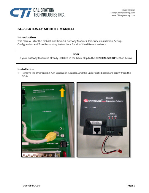
GG-6 GATEWAY MODULE MANUALIntroductionThis manual is for the GG6-GE and GG6-GR Gateway Modules. It includes Installation, Set-up, Configuration and Troubleshooting instructions for all of the different variants.NOTEIf your Gateway Module is already installed in the GG-6, skip to the GENERAL SET-UP section below. Installation1.Remove the Unitronix EX-A2X Expansion Adapter, and the upper right backboard screw from theGG-6.2.Place the GG-6 Gateway where the ExpansionAdapter was located and loosely attach the upper right screw.3.Re-install the Expansion Adapter, tighten allscrews, and re-connect the power andcommunication cables.4.Cut the zip ties along the Expansion Adapter communication cable, and install the newcommunication/power cable alongside the Expansion Adapter cable.5.Run the power cable (Orange, White/Orange pair) up to the top connector on the GG-6 PLC.6.Double up the Orange wire with the Red wire in the first terminal position on the PLC. Double upthe White/Orange wire with the Black wire in the second terminal position.7.Plug the Blue, White/Blue pair of wires with the RJ-11 connector into Port 2 (the RS-485 port) on thePLC.8.Reinstall any zip ties that were removed.General Set UpPower up the GG-6 and check the GG-6 MODBUS Configuration (see GG-6 Manual for menu navigation): ID (64 to 127): 64Master/Slave: SlaveDisplay: MainDownload and install the ICC Configuration Studio SW ver 2.0.3.7 on a PC, running Win 7 or higher. The computer will need a spare USB Port. The program can be found on the CTI website athttps:///Downloads. Scroll down to the Tools section at the bottom of the page and download ICC Configuration Studio V2.0.3.7 Installer. Un-Zip the file and install the program.Run the ICC Configuration Studio program. Do not upgrade to a newer version of ICC Configuration Studio.Connect the GG-6 Gateway Module to the computer using the mini-USB cable.Check for data activity in Database.Once connected, the Online Devices should show one new device under the Device Configurations.Select the Online Devices, and select the Discovered Devices tab. Double click on the ETH-1000 (for the GG6-GE-x) or the XLTR-1000 (for the GG6-GR-x), and select the Project tab.Right click on ETH-1000 or XLTR-1000 and select Upload Configuration.CAUTIONDo not change any parameters, other than directed, within the GG-6 Gateway Module or you maycompromise the performance and safety of the GG-6.GG6-GE-E ConfigurationSelect the Ethernet tab on the uploaded ETH-1000 configuration.From this tab the IP Settings can be changed from Static to DHCP. In the Static mode, the IP Address, the Subnet Mask and the Default Gateway can be set.Select the EtherNet/IP Server tab on the uploaded ETH-1000 configuration.From this tab the Device Name and Connection Timeout Options can be set.Do not change anything on or below the Class 1 I/O Messaging tab.Once all of the changes have been made, right click on uploaded ETH-1000 configuration and select Download Configuration. Answer Yes to overwriting the configuration. Remove the mini-USB cable and close the program.GG6-GE-M ConfigurationSelect the Ethernet tab on the uploaded ETH-1000 configuration.From this tab the IP Settings can be changed from Static to DHCP. In the Static mode, the IP Address, the Subnet Mask and the Default Gateway can be set.Select the Modbus/TCP Server tab on the uploaded ETH-1000 configuration.From this tab the Timeout and Connection Timeout Options can be set.Do not change anything below the Node tab.Once all of the changes have been made, right click on uploaded ETH-1000 configuration and select Download Configuration. Answer Yes to overwriting the configuration. Remove the mini-USB cable and close the program.GG6-GE-B ConfigurationSelect the Ethernet tab on the uploaded ETH-1000 configuration.From this tab the IP Settings can be changed from Static to DHCP. In the Static mode, the IP Address, the Subnet Mask and the Default Gateway can be set.Select the BACnet/IP Server tab on the uploaded ETH-1000 configuration.From this tab the UDP Port, APDU Timeout and the Number of APDU Retries can be set.Select the Device Object tab under the Node tab on the uploaded ETH-1000 configuration.From this tab the Device Name and the Instance Number can be changed.Do not change anything below the Device Object tab.Once all of the changes have been made, right click on uploaded ETH-1000 configuration and select Download Configuration. Answer Yes to overwriting the configuration. Remove the mini-USB cable and close the program.GG6-GR-M ConfigurationSelect the Modbus RTU Slave tab on the uploaded XLTR-1000 configuration.From this tab the Baud Rate, Parity, Timeout and Response Delay can be set to match the RS-485 network.Select the Node tab on the on the uploaded XLTR-1000 configuration.From this tab the Modbus Address can be set.Do not change anything below the Node tab.Once all of the changes have been made, right click on uploaded XLTR-1000 configuration and select Download Configuration. Answer Yes to overwriting the configuration. Remove the mini-USB cable and close the program.GG6-GR-B ConfigurationSelect the BACnet MS/TP Server tab on the uploaded XLTR-1000 configuration.From this tab the Baud Rate, Parity and Max Master can be set to match the RS-485 network.Select the Node tab on the on the uploaded XLTR-1000 configuration.From this tab the MAC Address can be set.Select the Device Object tab on the uploaded XLTR-1000 configuration.From this tab the Device Name and the Instance Number can be set.Do not change anything below the Device Object tab.Once all of the changes have been made, right click on uploaded XLTR -1000 configuration and select Download Configuration. Answer Yes to overwriting the configuration. Remove the mini-USB cable and close the program.TroubleshootingDownload the appropriate Help Manual from the ICC Configuration Studio.Help >> Help Manuals >> select from table below:GG6-GE-E ETH-1000 >> EtherNet/IP Server Driver ManualGG6-GE-M ETH-1000 >> Modbus/TCP Server Driver ManualGG6-GE-B ETH-1000 >> BACnet/IP Server Driver ManualGG6-GR-M XLTR-1000 >> Modbus RTU Slave Driver ManualGG6-GR-B XLTR-1000 >> BACnet MS/TP Server Driver ManualCheck the MODBUS Configuration on the GG-6.With the USB cable connected, check for data activity in Database section of the ICC Configuration Studio.GG6-GE-E Register MapIf connecting to a ControlLogix PLC (such as a 1756-L61) coupled with a 1756-ENBT/A comm interface, follow the example in Sec 1.5.3 starting on pg 11 of the “EtherNet/IP Server Driver Manual” (see pg. 12 above for help finding the Driver Manual).Use the CIP Data Table Read message type.Use the Data Type INT (16 bit) and the Database addresses.On pg 12 step g), change the Data Type to INT[194].Description DBAddress Data Type SourceElementNum ofElementsDest ElementSignal Data (1,2) 0 16-Bit Unsigned DB_w_0 30 data_array[0] Fault Discretes (3) 60 16-Bit Unsigned DB_w_60 2 data_array[30] Warn Discretes (3) 64 16-Bit Unsigned DB_w_64 2 data_array[32] Alarm1 Discretes (3) 68 16-Bit Unsigned DB_w_68 2 data_array[34] Alarm2 Discretes (3) 72 16-Bit Unsigned DB_w_72 2 data_array[36] Relay Discretes (3) 76 16-Bit Unsigned DB_w_76 2 data_array[38] STEL Data (2) 100 16-Bit Unsigned DB_w_100 30 data_array[40] STEL Discretes (3) 160 16-Bit Unsigned DB_w_160 2 data_array[70] TWA Data (2) 200 16-Bit Unsigned DB_w_200 30 data_array[72] TWA Discretes (3) 260 16-Bit Unsigned DB_w_260 2 data_array[102] Warn Setpoint (2,4) 300 16-Bit Unsigned DB_w_300 30 data_array[104] Alarm1 Setpoint (2,4) 360 16-Bit Unsigned DB_w_360 30 data_array[134] Alarm2 Setpoint (2,4) 420 16-Bit Unsigned DB_w_420 30 data_array[164] Notes: (1) Signal data from Sensor channels.(2) Data represents values displayed on the GG-6. If the range is less than 10 then the signalneeds to be divided by 100. If the range is greater than or equal to 10 and less than 100then the signal needs to be divided by 10.(3) 30 discretes are packed into two 16 bit words.(4) Setpoints are read only.GG6-GE-M Register MapDescription StartRegister Number ofRegistersModbusAddress Data TypeSignal Data (1,2,3) 30001 30 0 16-Bit Unsigned Fault Discretes (4) 30061 2 60 16-Bit Unsigned Warn Discretes (4) 30065 2 64 16-Bit Unsigned Alarm1 Discretes (4) 30069 2 68 16-Bit Unsigned Alarm2 Discretes (4) 30073 2 72 16-Bit Unsigned Relay Discretes (4) 30077 2 76 16-Bit Unsigned STEL Data (2,3) 30101 30 100 16-Bit Unsigned STEL Discretes (4) 30161 2 160 16-Bit Unsigned TWA Data (2,3) 30201 30 200 16-Bit Unsigned TWA Discretes (4) 30261 2 260 16-Bit Unsigned Warn Setpoint (2,3,5) 30301 30 300 16-Bit Unsigned Alarm1 Setpoint (2,3,5) 30361 30 360 16-Bit Unsigned Alarm2 Setpoint (2,3,5) 30421 30 420 16-Bit Unsigned Notes: (1) Signal data from Sensor channels.(2) Two registers numbers are used to represent each data value. For example, Sensor 1 =30001, Sensor 2 = 30003, Sensor 3 = 30005, etc.(3) Data represents values displayed on the GG-6. If the range is less than 10 then the signalneeds to be divided by 100. If the range is greater than or equal to 10 and less than 100then the signal needs to be divided by 10.(4) 30 discretes are packed into two 16 bit words.(5) Setpoints are read only.GG6-GE-B Register MapDescription ObjectName Instance Object Type Data TypeSignal Data (1,2) Sensor 1 -Sensor 300-29 Analog Input 16-Bit UnsignedFault Discretes (3) Faults 30 Multi-state Input 32-Bit Unsigned Warn Discretes (3) Warnings 31 Multi-state Input 32-Bit Unsigned Alarm1 Discretes (3) Alarm1s 32 Multi-state Input 32-Bit Unsigned Alarm2 Discretes (3) Alarm2s 33 Multi-state Input 32-Bit Unsigned Relay Discretes (3) Relays 34 Multi-state Input 32-Bit Unsigned STEL Data (2) STEL 1 -STEL 3040-69 Analog Input 16-Bit UnsignedSTEL Discretes (3) STELAlarms70 Multi-state Input 32-Bit UnsignedTWA Data (2) TWA 1 -TWA 3080-109 Analog Input 16-Bit UnsignedTWA Discretes (3) TWAAlarms110 Multi-state Input 32-Bit UnsignedSessions Count (4) SessionsCount120 Multi-state Input 32-Bit UnsignedNotes: (1) Signal data from Sensor channels.(2) Data represents values displayed on the GG-6. If the range is less than 10 then the signalneeds to be divided by 100. If the range is greater than or equal to 10 and less than 100then the signal needs to be divided by 10.(3) 30 discretes are packed into two 16 bit words.(4) Sessions Count is a counter that increments every time the GG-6 communicates with theGateway Module. This can be used as a watchdog timer.GG6-GR-M Register MapDescriptionStartRegisterNumber ofRegistersModbusAddress Data TypeSignal Data (1,2,3) 30001 30 0 16-Bit Unsigned Fault Discretes (4) 30061 2 60 16-Bit Unsigned Warn Discretes (4) 30065 2 64 16-Bit Unsigned Alarm1 Discretes (4) 30069 2 68 16-Bit Unsigned Alarm2 Discretes (4) 30073 2 72 16-Bit Unsigned Relay Discretes (4) 30077 2 76 16-Bit Unsigned STEL Data (2,3) 30101 30 100 16-Bit Unsigned STEL Discretes (4) 30161 2 160 16-Bit Unsigned TWA Data (2,3) 30201 30 200 16-Bit Unsigned TWA Discretes (4) 30261 2 260 16-Bit Unsigned Warn Setpoint (2,3,5) 30301 30 300 16-Bit Unsigned Alarm1 Setpoint (2,3,5) 30361 30 360 16-Bit Unsigned Alarm2 Setpoint (2,3,5) 30421 30 420 16-Bit Unsigned Notes: (1) Signal data from Sensor channels.(2) Two registers numbers are used to represent each data value. For example, Sensor 1 =30001, Sensor 2 = 30003, Sensor 3 = 30005, etc.(3) Data represents values displayed on the GG-6. If the range is less than 10 then the signalneeds to be divided by 100. If the range is greater than or equal to 10 and less than 100then the signal needs to be divided by 10.(4) 30 discretes are packed into two 16 bit words.(5) Setpoints are read only.GG6-GR-B Register MapDescription ObjectName Instance Object Type Data TypeSignal Data (1,2) Sensor 1 -Sensor 300-29 Analog Input 16-Bit UnsignedFault Discretes (3) Faults 30 Multi-state Input 32-Bit Unsigned Warn Discretes (3) Warnings 31 Multi-state Input 32-Bit Unsigned Alarm1 Discretes (3) Alarm1s 32 Multi-state Input 32-Bit Unsigned Alarm2 Discretes (3) Alarm2s 33 Multi-state Input 32-Bit Unsigned Relay Discretes (3) Relays 34 Multi-state Input 32-Bit Unsigned STEL Data (2) STEL 1 -STEL 3040-69 Analog Input 16-Bit UnsignedSTEL Discretes (3) STELAlarms70 Multi-state Input 32-Bit UnsignedTWA Data (2) TWA 1 -TWA 3080-109 Analog Input 16-Bit UnsignedTWA Discretes (3) TWAAlarms110 Multi-state Input 32-Bit UnsignedSessions Count (4) SessionsCount120 Multi-state Input 32-Bit UnsignedNotes: (1) Signal data from Sensor channels.(2) Data represents values displayed on the GG-6. If the range is less than 10 then the signalneeds to be divided by 100. If the range is greater than or equal to 10 and less than 100then the signal needs to be divided by 10.(3) 30 discretes are packed into two 16 bit words.(4) Sessions Count is a counter that increments every time the GG-6 communicates with theGateway Module. This can be used as a watchdog timer.。
A4503
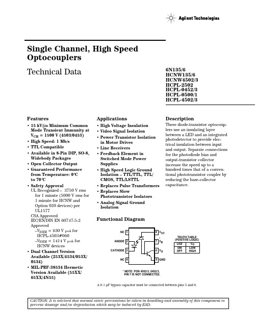
Single Channel, High Speed Optocouplers Technical DataFeatures• 15 kV/µs Minimum Common Mode Transient Immunity at V CM = 1500 V (4503/0453)• High Speed: 1 Mb/s • TTL Compatible• Available in 8-Pin DIP, SO-8,Widebody Packages • Open Collector Output • Guaranteed Performance from Temperature: 0°C to 70°C• Safety ApprovalUL Recognized – 3750 V rms for 1 minute (5000 V rms for 1 minute for HCNW and Option 020 devices) per UL1577CSA ApprovedIEC/EN/DIN EN 60747-5-2Approved–V IORM = 630 V peak for HCPL-4503#060–V IORM = 1414 V peak for HCNW devices• Dual Channel VersionAvailable (253X/4534/053X/0534)• MIL-PRF-38534 Hermetic Version Available (55XX/65XX/4N55)Applications• High Voltage Insulation • Video Signal Isolation• Power Transistor Isolation in Motor Drives • Line Receivers• Feedback Element in Switched Mode Power Supplies• High Speed Logic Ground Isolation – TTL/TTL, TTL/CMOS, TTL/LSTTL• Replaces Pulse Transformers • Replaces SlowPhototransistor Isolators • Analog Signal Ground IsolationDescriptionThese diode-transistor optocoup-lers use an insulating layerbetween a LED and an integrated photodetector to provide elec-trical insulation between input and output. Separate connections for the photodiode bias and output-transistor collector increase the speed up to ahundred times that of a conven-tional phototransistor coupler by reducing the base-collector capacitance.Functional Diagram6N135/6HCNW135/6HCNW4502/3HCPL-2502HCPL-0452/3HCPL-0500/1HCPL-4502/3CAUTION: It is advised that normal static precautions be taken in handling and assembly of this component to prevent damage and/or degradation which may be induced by ESD.A 0.1 µF bypass capacitor must be connected between pins 5 and 8.V CC V B V O GND** NOTE: FOR 4502/3, 0452/3,PIN 7 IS NOT CONNECTED.TRUTH TABLE (POSITIVE LOGIC)LEDONOFFV O LOW HIGHGNDV CCOANODECATHODEB* NOTE: FOR HCPL-4502/-3, HCPL-0452/3, HCNW4502/3, PIN 7 IS NOT CONNECTED.Ordering InformationSpecify Part Number followed by Option Number (if desired).Example:HCPL-4503#XXXX020 =UL 5000 V rms/1 Minute Option*060 =IEC/EN/DIN EN 60747-5-2 V IORM = 630 V peak Option**300 =Gull Wing Surface Mount Option†500 =Tape and Reel Packaging Option XXXE = Lead Free OptionOption data sheets available. Contact your Agilent sales representative or authorized distributor for information.*For 6N135/6 and HCPL-4502/3 only.**For HCPL-4503 only. Combination of Option 020 and Option 060 is not available.†Gull wing surface mount option applies to through hole parts only.*Technical data for these products are on separate Agilent publications.†Pin 7, transistor base, is not connected.output current for 1 TTL load and a 5.6 k Ω pull-up resistor. CTR for these devices is 19% minimum at I F =16mA.The HCPL-4502, HCPL-0452,and HCNW4502 provide the electrical and switching performance of the 6N136,HCPL-0501, and HCNW136 with increased ESD protection.The HCPL-4503, HCPL-0453,and HCNW4503 are similar to the HCPL-4502, HCPL-0452, and HCNW4502 optocouplers but have increased common mode transient immunity of 15 kV/µs minimum at V CM =1500V guaranteed.These single channel optocoup-lers are available in 8-Pin DIP,SO-8 and Widebody package configurations.The 6N135, HCPL-0500, and HCNW135 are for use in TTL/CMOS, TTL/LSTTL or wide bandwidth analog applications.Current transfer ratio (CTR) for these devices is 7% minimum at I F =16mA.The 6N136, HCPL-2502,HCPL-0501, and HCNW136 are designed for high speed TTL/TTL applications. A standard 16 mA TTL sink current through the input LED will provide enoughRemarks: The notation “#” is used for existing products, while (new) products launched since 15th July 2001 and lead free option will use “-”Package Outline Drawings8-Pin DIP Package (6N135/6, HCPL-4502/3, HCPL-2502)8-Pin DIP Package with Gull Wing Surface Mount Option 300 (6N135/6, HCPL-4502/3)0.254+ 0.076- 0.051(0.010+ 0.003)- 0.002)DIMENSIONS IN MILLIMETERS AND (INCHES).*MARKING CODE LETTER FOR OPTION NUMBERS "L" = OPTION 020"V" = OPTION 060OPTION NUMBERS 300 AND 500 NOT MARKED.NOTE: FLOATING LEAD PROTRUSION IS 0.25 mm (10 mils) MAX.(0.025 ± 0.005)(0.100)BSCDIMENSIONS IN MILLIMETERS (INCHES).LEAD COPLANARITY = 0.10 mm (0.004 INCHES).NOTE: FLOATING LEAD PROTRUSION IS 0.25 mm (10 mils) MAX.+ 0.076- 0.051+ 0.003)- 0.002)Small Outline SO-8 Package (HCPL-0500/1, HCPL-0452/3)8-Pin Widebody DIP Package (HCNW135/6, HCNW4502/3)(0.012)MIN.5.207 ± 0.254 (0.205 ± 0.010)DIMENSIONS IN MILLIMETERS (INCHES).LEAD COPLANARITY = 0.10 mm (0.004 INCHES) MAX.*1.78 ± 0.15NOTE: FLOATING LEAD PROTRUSION IS 0.25 mm (10 mils) MAX.0.254+ 0.076- 0.0051+ 0.003)- 0.002)8-Pin Widebody DIP Package with Gull Wing Surface Mount Option 300 (HCNW135/6,HCNW4502/3)Solder Reflow Temperature ProfileTIME (SECONDS)T E M P E R A T U R E (°C )ROOM1.78 ± 0.15MAX.BSCDIMENSIONS IN MILLIMETERS (INCHES).LEAD COPLANARITY = 0.10 mm (0.004 INCHES).NOTE: FLOATING LEAD PROTRUSION IS 0.25 mm (10 mils) MAX.Regulatory InformationThe devices contained in this data sheet have been approved by the following organizations:ULRecognized under UL 1577,Component Recognition Program, File E55361.CSAApproved under CSA Component Acceptance Notice #5, File CA 88324.Insulation and Safety Related Specifications8-Pin DIP Widebody (300 Mil)SO-8(400 Mil)Parameter Symbol Value Value Value Units ConditionsMinimum External L(101)7.14.99.6mmMeasured from input terminals Air Gap (External to output terminals, shortest Clearance)distance through air.Minimum External L(102)7.4 4.810.0mmMeasured from input terminals Tracking (External to output terminals, shortest Creepage)distance path along body.Minimum Internal 0.080.08 1.0mmThrough insulation distance,Plastic Gapconductor to conductor, usually (Internal Clearance)the direct distance between the photoemitter and photodetector inside the optocoupler cavity.Minimum Internal NA NA 4.0mmMeasured from input terminals Tracking (Internal to output terminals, along Creepage)internal cavity.Tracking Resistance CTI 200200200VoltsDIN IEC 112/VDE 0303 Part 1(Comparative Tracking Index)Isolation GroupIIIa IIIa IIIaMaterial Group(DIN VDE 0110, 1/89, Table 1)Option 300 - surface mount classification is Class A in accordance with CECC 00802.IEC/EN/DIN EN 60747-5-2Approved underIEC 60747-5-2:1997 + A1:2002EN 60747-5-2:2001 + A1:2002DIN EN 60747-5-2 (VDE 0884 Teil 2):2003-01(HCNW and Option 060 only)Recommended Pb-Free IR Profile°C of ACTUAL NOTES:THE TIME FROM 25 °C to PEAK TEMPERATURE = 8 MINUTES MAX.T smax = 200 °C, T smin = 150 °CIEC/EN/DIN EN 60747-5-2 Insulation Related Characteristics(HCPL-4503 OPTION 060 ONLY)IEC/EN/DIN EN 60747-5-2 Insulation Related Characteristics (HCNW135/6, HCNW4502/3 ONLY)*Refer to the front of the optocoupler section of the current catalog, under Product Safety Regulations section IEC/EN/DIN EN60747-5-2, for a detailed description.Note: Isolation characteristics are guaranteed only within the safety maximum ratings which must be ensured by protective circuits in application.*Data has been registered with JEDEC for the 6N135/6N136.Electrical Specifications (DC)Over recommended temperature (T A = 0°C to 70°C) unless otherwise specified. See note 13.Parameter Symbol Device Min.Typ.**Max.Units Test Conditions Fig.Note Current CTR*6N13571850%T A = 25°C V O = 0.4 V I F = 16 mA,1, 2,5, 11 Transfer Ratio HCPL-0500V CC = 4.5 V4HCNW135519V O = 0.5 VHCPL-25021522T A = 25°C V O = 0.4 V1525V O = 0.5 V6N136192450T A = 25°C V O = 0.4 VHCPL-4502/3HCPL-05011525V O = 0.5 VHCPL-0452/3HCNW136HCNW4502/3Logic Low V OL6N1350.10.4V T A = 25°C I O = 1.1 mA I F = 16 mA,Output Voltage HCPL-0500V CC = 4.5 VHCNW1350.10.5I O = 0.8 mA6N1360.10.4T A = 25°C I O = 3.0 mAHCPL-2502HCPL-4502/30.10.5I O = 2.4 mAHCPL-0501HCPL-0452/3HCNW136HCNW4502/3Logic High I OH*0.0030.5µA T A = 25°C V O = V CC = 5.5 V I F = 0 mA7Output Current0.011T A = 25°C V O = V CC = 15 V50V O = V CC = 15 VLogic Low I CCL50200µA I F = 16 mA, V O = Open, V CC = 15 V13 Supply CurrentLogic High I CCH*0.021µA T A = 25°C I F = 16 mA, V O = Open,13 Supply Current2V CC = 15 VInput Forward V F*8-Pin DIP 1.5 1.7V T A = 25°C I F = 16 mA3Voltage SO-8 1.8Widebody 1.45 1.68 1.85T A = 25°C I F = 16 mA1.35 1.95Input Reverse BV R*8-Pin DIP5V I R = 10 µABreakdown SO-8Voltage Widebody3I R = 100 µATemperature∆V F/8-Pin DIP-1.6mV/°C I F = 16 mACoefficient of∆T A SO-8Forward Voltage Widebody-1.9Input C IN8-Pin DIP60pF f = 1 MHz, V F = 0 VCapacitance SO-8Widebody90Transistor DC h FE8-Pin DIP150V O = 5 V, I O = 3 mACurrent Gain SO-8130V O = 0.4 V, I B = 20 µAWidebody180V O = 5 V, I O = 3 mA160V O = 0.4 V, I B = 20 µA*For JEDEC registered parts.**All typicals at T A = 25°C.Parameter Sym.Device Min.Typ.**Max.Units Test ConditionsFig.Note Propagation t PHL *6N1350.2 1.5µs T A = 25°C R L = 4.1 k Ω5, 6,8, 9HCPL-0500 2.011HCNW1356N1360.20.8T A = 25°C R L = 1.9 k ΩHCPL-2502HCPL-4502/3HCPL-0501HCPL-0452/3 1.0HCNW136HCNW4502/3Propagation t PLH *6N135 1.3 1.5µsT A = 25°C R L = 4.1 k Ω5, 6,8, 9HCPL-0500 2.011HCNW1356N1360.60.8T A = 25°C R L = 1.9 k ΩHCPL-2502HCPL-4502/3HCPL-0501HCPL-0452/3 1.0HCNW136HCNW4502/3Common Mode |CM H |6N1351kV/µs R L = 4.1 k ΩI F = 0 mA, T A = 25°C,127, 8,HCPL-0500V CM = 10 V p-p 9HCNW135C L = 15 pF6N1361R L = 1.9 k ΩHCPL-2502HCPL-4502HCPL-0501HCPL-0452HCNW4502HCPL-45031530R L = 1.9 k ΩI F = 0 mA, T A = 25°C,HCPL-0453V CM = 1500 V p-p ,HCNW4503C L = 15 pFCommon Mode |CM L |6N1351kV/µs R L = 4.1 k ΩI F = 16 mA, T A = 25°C,127, 8,HCPL-0500V CM = 10 V p-p 9HCNW135C L = 15 pF6N1361R L = 1.9 k ΩHCPL-2502HCPL-4502HCPL-0501HCPL-0452HCNW4502HCPL-45031530R L = 1.9 k ΩI F = 16 mA, T A = 25°C,HCPL-0453V CM = 1500 V p-p ,HCNW4503C L = 15 pFBandwidth BW 6N135/69MHzSee Test Circuit8, 1010HCPL-2502HCPL-0500/1HCNW135/611*For JEDEC registered parts.**All typicals at T A = 25°C.Switching Specifications (AC)Over recommended temperature (T A = 0°C to 70°C), V CC = 5 V, I F = 16 mA unless otherwise specified.Delay Time to Logic Low at OutputDelay Time to Logic High at OutputTransient Immunity at Logic High Level OutputTransient Immunity at Logic Low Level OutputPackage CharacteristicsOver recommended temperature (T A = 0°C to 70°C) unless otherwise specified.*All typicals at T A = 25°C.**The Input-Output Momentary Withstand Voltage is a dielectric voltage rating that should not be interpreted as an input-output continuous voltage rating. For the continuous voltage rating refer to the IEC/EN/DIN EN 60747-5-2 Insulation Related Characteristics Table (if applicable), your equipment level safety specification or Agilent Application Note 1074 entitled “Optocoupler Input-Output Endurance Voltage,” publication number 5963-2203E.Notes:1.Derate linearly above 70°C free-air temperature at a rate of 0.8 mA/°C (8-Pin DIP).Derate linearly above 85°C free-air temperature at a rate of 0.5 mA/°C (SO-8).2.Derate linearly above 70°C free-air temperature at a rate of 1.6 mA/°C (8-Pin DIP).Derate linearly above 85°C free-air temperature at a rate of 1.0 mA/°C (SO-8).3.Derate linearly above 70°C free-air temperature at a rate of 0.9 mW/°C (8-Pin DIP).Derate linearly above 85°C free-air temperature at a rate of 1.1 mW/°C (SO-8).4.Derate linearly above 70°C free-air temperature at a rate of 2.0 mW/°C (8-Pin DIP).Derate linearly above 85°C free-air temperature at a rate of 2.3 mW/°C (SO-8).5.CURRENT TRANSFER RATIO in percent is defined as the ratio of output collector current, I O, to the forward LED input current, I F,times 100.6.Device considered a two-terminal device: Pins 1, 2, 3, and 4 shorted together and Pins 5, 6, 7, and 8 shorted together.mon mode transient immunity in a Logic High level is the maximum tolerable (positive) dV CM/dt on the leading edge of thecommon mode pulse signal, V CM, to assure that the output will remain in a Logic High state (i.e., V O > 2.0 V). Common mode transient immunity in a Logic Low level is the maximum tolerable (negative) dV CM/dt on the trailing edge of the common mode pulse signal, V CM, to assure that the output will remain in a Logic Low state (i.e., V O < 0.8 V).8.The 1.9 kΩ load represents 1 TTL unit load of 1.6 mA and the 5.6 kΩ pull-up resistor.9.The 4.1 kΩ load represents 1 LSTTL unit load of 0.36 mA and 6.1 kΩ pull-up resistor.10.The frequency at which the ac output voltage is 3 dB below its mid-frequency value.11.The JEDEC registration for the 6N136 specifies a minimum CTR of 15%. Agilent guarantees a minimum CTR of 19%.12.See Option 020 data sheet for more information.e of a 0.1 µf bypass capacitor connected between pins 5 and 8 is recommended.14.In accordance with UL 1577, each optocoupler is proof tested by applying an insulation test voltage ≥ 4500 V rms for 1 second(leakage detection current limit, I I-O≤ 5 µA). This test is performed before the 100% Production test shown in the IEC/EN/DIN EN 60747-5-2 Insulation Related Characteristics Table if applicable.15.In accordance with UL 1577, each optocoupler is proof tested by applying an insulation test voltage ≥ 6000 V rms for 1 second(leakage detection current limit, I I-O≤ 5 µA). This test is performed before the 100% Production test shown in the IEC/EN/DIN EN 60747-5-2 Insulation Related Characteristics Table if applicable.16.This rating is equally validated by an equivalent ac proof test.Figure 2. Current Transfer Ratio vs. Input Current.Figure 3. Input Current vs. Forward Voltage.Figure 1. DC and Pulsed Transfer Characteristics.105V O – OUTPUT VOLTAGE – VI O – O U T P U T C U R R E N T – m A8 PIN DIP, SO-8128V O – OUTPUT VOLTAGE – VI O – O U T P U T C U R R E N T – m A416WIDEBODY1.51.00.5N O R M A L I Z E D C U R R E N T T R A N S F E R R A T I OI F – INPUT CURRENT – mA8 PIN DIP, SO-80N O R M A L I Z E D C U R R E N T T R A N S F E R R A T I OI F – INPUT CURRENT – mA1.50.51.0WIDEBODYV F – FORWARD VOLTAGE –VOLTS I F – F O R W A R D C U R R E N T – m A8 PIN DIP, SO-8V F –FORWARD VOLTAGE – VOLTS1000100101.00.10.001I F – F O R W A R D C U R R E N T – m AWIDEBODYFigure 6. Propagation Delay Time vs. Load Resistance.Figure 5. Propagation Delay vs. Temperature.Figure 4. Current Transfer Ratio vs. Temperature.1.00.90.80.70.6N O R M A L I Z E D C U R R E N T T R A N S F E R R A T I OT A – TEMPERATURE – °C 8 PIN DIP, SO-81.11.00.90.80.70.660N O R M A L I Z E D C U R R E N T T R A N S F E R R A T I OT A – TEMPERATURE – °C0.50.4WIDEBODY1.0R L – LOAD RESISTANCE – (k Ω)t P – P R O P A G A T I O N D E L A Y – µs8 PIN DIP, SO-8R L – LOAD RESISTANCE – (k Ω)t P – P R O P A G A T I O N D E L A Y – µs6.04.01.00.60.40.2WIDEBODY150010005000t p – P R O P A G A T I O N D E L A Y – n sT A – TEMPERATURE – °C 8 PIN DIP, SO-81000800600400200T A – TEMPERATURE – °CWIDEBODYt p – P R O P A G A T I O N D E L A Y – n sFigure 9. Thermal Derating Curve, Dependence of Safety Limiting Value with Case Temperature per IEC/EN/DIN EN 60747-5-2.Figure 8. Small-Signal Current Transfer Ratio vs. Quiescent Input Current.Figure 7. Logic High Output Current vs. Temperature.T A – TEMPERATURE – °C10+410101001010+210+3I O H – L O G I C H I G H O U T P U T C U R R E N T – n A8 PIN DIP, SO-8I O H– L O G I C H I G H O U T P U T C U R R E N T – n AT A – TEMPERATURE – °C10101010WIDEBODY∆ I F∆I O – S M A L L S I G N A L C U R R E N T T R A N S F E R R A T I O I F – QUIESCENT INPUT CURRENT – mA 8 PIN DIP, SO-80.30∆ I F ∆ I O– S M A L L S I G N A L C U R R E N T T R A N S F E R R A T I OI F – QUIESCENT INPUT CURRENT – mAWIDEBODYO U T P U TP O W E R – P S , I N P U T C U R R E N T – I ST S – CASE TEMPERATURE – °C O U T P U T P OW E R – P S , I N P U T C U R R E N T – I S0T S – CASE TEMPERATURE – °C1000400600800200100300500700900Figure 10. Frequency Response.HCNW135/6HCNW135/60.11.010100-20-15-10-5+5T A = 25 °Cf - FREQUENCY - MHzN O R M A L I Z E D R E S P O N S E - d B6N135/6, HCPL-0500/1, HCPL-2502V TYPICAL I = 9 mA FO6N135/6, HCPL-0500/1, HCPL-2502Figure 12. Test Circuit for Transient Immunity and Typical Waveforms.Figure 11. Switching Test Circuit.OF= 1.5 µFt V I F OVOV O/semiconductorsFor product information and a complete list ofdistributors, please go to our web site.For technical assistance call:Americas/Canada: +1 (800) 235-0312 or (916) 788-6763Europe: +49 (0) 6441 92460China: 10800 650 0017Hong Kong: (+65) 6756 2394India, Australia, New Zealand: (+65) 6755 1939Japan: (+81 3) 3335-8152 (Domestic/Interna-tional), or 0120-61-1280 (Domestic Only)Korea: (+65) 6755 1989Singapore, Malaysia, Vietnam, Thailand,Philippines, Indonesia: (+65) 6755 2044Taiwan: (+65) 6755 1843Data subject to change.Copyright © 2004 Agilent Technologies, Inc.Obsoletes 5989-0305EN December 20, 20045989-2112EN。
七年级上册英语单词拆分速记法

七年级上册英语单词拆分速记法name 联想方式:na:那;me:我记忆方法:你们都有英文名字了,那我叫什么名字呢?clock 联想方式:clo-(骷髅);ck-(刺客)记忆方法:骷髅刺客站钟上。
nice 联想方式:ni:你ce:厕所记忆方法:你的厕所很漂亮meet 联想方式:m:妈ee:眼睛t:雨伞记忆方法:妈睁开两只眼睛就看到(遇见)雨伞you 联想方式:you-游记忆方法:我和你一起去旅游吧。
what 联想方式:w:我;hat:帽子记忆方法:猜,我帽子里有什么?hello 联想方式:he:他;llo:110 记忆方法:他打电话给110说“喂”。
and 联想方式:a:一;nd:牛顿记忆方法:一个牛顿和另外一个牛顿,都不是真的牛顿。
her 联想方式:h花;er儿记忆方法:这花儿是她的歌迷送的question 联想方式:ques(缺少);tion(神)记忆方法:现在问题是缺少神的庇佑。
Answer 联想方式:an:一个;sw(上网);er儿子记忆方法:一个正在上网的儿子是不会回答你问题的look 联想方式:loo-100k-机关枪记忆方法:100支机关枪看起来很壮观. first 联想方式:f—发i—蜡烛rst—瑞士糖记忆方法:首先发蜡烛,用蜡烛烧瑞士糖last(n. 最后;上个adj. 最后的;最近的,最新的vi. 持续;持久vt. 度过,拖过;使维持adv. 最后;上次,最近地)联想方式:la—拉st—石头记忆方法:我们的工作就是一直地拉石头。
boy 联想方式:bo-(伯)y-(形状像衣叉)记忆方法:伯伯用衣叉打男孩girl 联想方式:g:哥哥;i:爱;rl:日历记忆方法:哥哥爱上了日历中的女孩。
zero 联想方式:ze—(选)择记忆方法:选择零度的肉会更好one 联想方式:one:谐音“玩”记忆方法:第一名就可以去玩了。
two 联想方式:two:兔子记忆方法:有2只兔子。
three 联想方式:tree-(树);h-(椅)记忆方法:树中间有三椅子。
美国卡麦隆管线球阀产品样本

C O O P E R C A M E R O N V A LV ES1FULLY WELDED BALL VALVESFULLY WELDED BALL VALVES Features and Benefits2, 3, 4 & 5In-line Sphere Launcher 6Accessories7HOW TO ORDER Standards, Specifications and Materials 8 & 9DIMENSION TABLES ASME/ANSI Class 150 through 2500 (PN 20 through PN 420)Full and Reduced Port Valves 10 through 22API PRESSURE CLASS 2000, 3000 & 5000 psiFull and Reduced Port Valves23, 24 & 25DIMENSION TABLES Actuator Mounting Information26, 27 & 28PIPING INFORMATION TABLE29TERMS AND CONDITIONS30 & 31TRADEMARK INFORMATION32TABLE OF CONTENTSTC145512/04 NP-5MP卡 麦 隆 全 焊 接 球 阀目 录全焊接球阀特点和优点管线清管球发送器附件如何购买卡麦隆球阀标准、规范和材料尺寸表全通径和缩径球阀全通径和缩径球阀尺寸表执行机构安装信息管子尺寸表商务条款和条件商标信息CO O P E R C A M E R O N V A LV E S2Engineered for heavy duty, maintenance free performance, the Cameron Fully Welded Ball Valve is commonly selected for a number of applications, including:One of the most trusted valves in the petroleum industry, itcombines the strength of forged components with a lightweight and compact spherical design.Cameron Fully Welded Ball Valves satisfy ASME/ANSI 150 through 2500 (PN 20 through PN 420) and API 2000 through10,000 standards. Made of forged steel to assure uniform fine grain structure and toughness, they may be specified in sizes from 2 in. to 56 in. (50 mm to 1400 mm).FEATURES AND BENEFITS•Gas transmission •NGL plants •Products pipeline •NGL pipeline •Measurements skids •Compressor stations •Dehydration systems •CO services 2•Gas separation systems •Offshore •Natural gas storage •Subsea•Dryer serviceTC145512/04 NP-5MFULLY WELDED BALL VALVES卡 麦 隆 全 焊 接 球 阀特 点 和 优 点石油工业中最值得信赖的阀门, 综合了轻型锻件的强度和紧凑式球形设计。
ARCGIS工具中英对照总结

Analysis Tool:分析工具Extract 提取Clip 剪切Select 选择Split拆分Table Select表选择Overlay叠加分析Erase 擦除Ide ntity 查看In tersect 相交SymmetricalDifferenee 对称差Union联合Update更新Proximity邻域分析Buffer缓冲区Multiple Ring Buffer 多环缓冲区Near 临近Point Distanee 点距离Statistics 统计表Frequency 频度Summary Statistics 总结统计Cartography Tool:绘图工具Masking Tools 掩模工具Cul-De-Sac Masks Cul- De-Sac 掩模Feature Outline Masks 要素xx掩模Intersecting Layers Masks 相交图层掩模Co nversion Tool:转换工具From Raster 从删格到... Raster to ASCI I 删格到ASCIIRaster to Float删格到浮点Raster to Point 删格到点Raster to Polygon 删格到面Raster to Polyline删格到线ArcGIS 9 ArcToolbox中英文对照表①3D An alyst Tools三维分析工具Conversion 转换TIN三角计算TIN域值TIN多边形标志TIN节点TIN边TIN到栅格栅格转TINFun cti onal Surface 表面功能插值形状表面体积表面点表面XX视线Raster In terpolati on 栅格修补克里XX地形到栅格曲线拟合用文件地形到栅格自然邻域趋势距离权重倒数Raster Math栅格计算乘减加取整浮点Raster ReclasS栅格重分类切片查找用ASCI I文件重分类用表重分类重分类Raster Surface 栅格表面坡向坡度填/挖山影曲率等高线等高线列表观察点视域Terrain地形地势地带领域TIN Creatio nTIN 创建创建TIN编辑TINTIN SurfaceTIN 表面TIN坡度TIN方位TIN等高线多边形插值成多个面②An alysis Tool分析工具Extract 提取Clip剪切Select选择Split拆分Table Select 表选择Overlay叠加分析Erase擦除Identity 查看Intersect 相交Symmetrical Difference 对称差Union联合Update更新Proximity邻域分析Buffer缓冲区Multiple Ring Buffer 多环缓冲区Near临近Poi nt Dista nee 点距离Statistics 统计表Freque ncy 频度Summary Statistics 总结统计③Cartography Too I绘图工具Maski ng Tools掩模工具Cul-De-Sac MasksCul-De-Sa掩模Feature Outline Masks要素xx 掩模In tersect ing Layers Masks 相交图层掩模④Conv ersi on Tool转换工具From Raster从删格到…Raster to ASCI删格到ASCIIRaster to Float删格到浮点Raster to Poi nt 删格到点Raster to Polygon 删格到面Raster to Polyli ne 删格到线To CAD到CADAdd CAD Fields添加CAD 字段Create CAD XData创建CAD扩展实体数据Export to CAD导出到CADSet CAD Alias设置CAD 别名To Coverage至U CoverageFeature Class To Coverage 要素类至U CoverageTo dBASE至dBASETable to dBASE [multiple]表到dBASETo GeodatabaseFeature Class To Feature Clas要素类到要素类Feature Class to Geodatabase [multiple] 要素类至U Geodatabase Import CAD Annotation 导入CAD 注记Import Coverage Annotation 导入Coverage 注记Import from CAD 从CAD 导入Raster To Geodatabase[multiple栅格至U GeodatabaseTable to Geodatabase[multiple]表至U GeodatabaseTable To Table表到表To Raster到栅格ASCII to RasterASCI 到栅格DEM to RasterDEM 到栅格Feature to Raster要素到栅格Float to Raster浮点到栅格Raster To Other Format栅格到其他格式To Shapefile到ShapefileFeature Class To Shapefile 要素类到Shapefile⑤Data In teroperability Tools 数据互转工具⑥Data Man ageme ntTools数据管理工具Database数据库Compact 紧凑Compress 压缩Disco nn ected Edit ing 分离编辑Check In 检入Check In From Delta从增量中检入Check Out 检出Export To Delta 导出增量Domai ns 值域Add Coded Value To Domair添加编码值到值域Assign Doma in To Fielc赋值值域到字段Create Doma in创建值域Delete Coded Value From Domain从值域中删除编码值Delete Doma in删除值域Domai n To Table 值域到表Remove Doma in From Field从字段删除值域Set Value For Ra nge Domain为范围值域设置值Table To Domai n 表到值域Feature class 要素类Append Annotation Feature Classes 追加注记要素类Calculate Default Cluster Toleranee 计算缺省容限值Calculate Default Spatial Grid Index 计算缺省空间格网xx Integrate 整合Update Anno tati on Feature Class更新标记要素类创建要素类创建要素类Features 要素Add XY Coordinates添加XY 坐标Cheek Geometry检查几何形状Copy Features复制要素Delete Features 删除要素Feature En velope to Polygon 要素圭寸装到多边形Feature To Li ne 要素到线Feature To Poi nt 要素到点Feature To Polygo n要素到多边形Feature Vertices To Poi nts要素定点至U点Multipart To Singlepart多部分到单部分Polygon To Line多边形到线Repair Geometry修改集合形状Split Li ne At Vertices 在定点拆分线Fields字段Add Field添加字段Assign Default To Fielc设置缺省到字段Calculate Field 计算字段Delete Field删除字段General —般Copy复制Delete删除Ren ame重命名Select Data选择数据追加追加Gen eralizati on —般Aggregate Polygo ns聚集多边形Collapse Dual Li nes To Cen terli ne 分解双线到中心线Dissolve 融合Eliminate 消除Smooth Line 平滑线Simplify Buildi ng 简化建筑物Simplify Line Or Polygon简化线或多边形IndexesxxAdd Attribute Index 添加属性xxAdd Spatial Index添加空间xx Remove Attribute Index 删除属性xx Remove Spatial Index删除空间xx Find Con flicts 查找冲突Drop Index 删除xxIn dex Itemxx 项Add Item添加项Drop Item删除项Joins连接Join Info Tables连接Info 表Projections 投影Define Projection 定义投影Project 投影Transform 变换Renu mber Nodes重新计数节点Update IDs更新IDTolera nces 容差Tolera nee 容差Topology拓扌卜Build构建Clea nClea nCreate Labels创建标注VPF Tile TopologyVPF图块拓扑Workspace Management 工作空间管理Create Coverage创建CoverageJoins连接Add Join添加连接Remove Join删除连接Layers and Table Views 图层和表的查看Make Query Table制作查询表Make Raster Catalog Laye制作栅格目录图层Make Raster Layer制作栅格图层Make XY Event Laye制作XY事件图层Save To Layer Fiie^存成图层文件Select Layer By Attribute 通过属性选择Select Layer By Location通过位置选择制作表视图制作表视图制作要素图层制作要素图层Projections and Transformations 投影和转换Feature 要素Batch Project批量投影Project 投影创建空间参考创建空间参考Raster栅格Flip翻转Mirror镜像Project Raster 投影栅格Rescale重建比例Rotate旋转Shift偏移War翘曲Define Projection 定义投影Raster栅格Batch Build Pyramids批量建立xxBatch Calculate Statistics批量计算统计表Build Pyramids建立xxCalculate Statistics 计算统计表Clip剪切Composite Bands 组合波段Copy Raster复制栅格Copy Raster Catalog Items复制栅格目录项Create Raster Catalog创建栅格目录Delete Raster Catalog Items 删除栅格目录项Mosaic To New Raster镶嵌到新的栅格Resample重采样创建栅格数据集创建栅格数据集镶嵌镶嵌Relati on ship Classes关系类Create Relatio nship Clas创建关系类Table To Relationship Class 表到关系类Subtypesxx 类型Add Subtype添加子类型Remove Subtype删除子类型Set Default Subtype设置缺省子类型Set Subtype Field设置子类型字段Table 表An alyze 分析Change Privileges改变权限Copy Rows复制行Delete Rows 删除行Get Cou nt获得数目Pivot Tablexx 表创建表创建表Topology拓扌卜Add Feature Class To Topology添加要素类型到拓扑Add Rule To Topology添加规则到拓扑Create Topology仓U建拓扌卜Remove Feature Class From Topology 从拓扌卜删除要素类Remove Rule From Topology从拓扑中删除规则Set Cluster Tolera nee设置簇容限值Validate Topology 教验拓扑Versions 版本Alter Version改变版本Create Version 创建版本Delete Versio n 删除版本Post Version提交版本Reeo ncile Versio n 协调版本Register As Versio nec注册版本Un register As Versioned 取消注册Workspace工作空间Create ArcInfo Workspace创建ArcInfo 工作空间Create Feature Dataset创J建要素数据集Create Folder创建文件夹Create Personal GDB创建个人GeodatabaseGeocodi ng Tools地理编码工具Automate Geocoding Indexes 自动生成地理编码xx Create Address Locator创建地址定位器Deautomate Geocoding Indexes取消自动生成地理编码xx Delete Address Locator删除地址定位器Geocode Addresses地理编码地址Rebuild Geocoding Indexes重建地理编码xxSta ndardize Addresses标准化地址⑦Geocoding Tools地理编码工具⑧Geostatistical Analyst Tools地理统计分析工具Geostatistical Layer To Grid 导出地理统计图层到Grid⑨Linear Referencing Tools线性参考工具Calibrate Routes 校准路径Create Routes创建路径Dissolve Route Eve nts融合路径事件Locate Features Alo ng Routes 沿路径定位要素Make Route Eve nt Layei制作路径事件图层Overlay Route Eve nts叠加路径事件Transform Route Eve nts 转换路径事件⑩Spatial An alyst Tools空间分析工具Conditional 条件拾取条件设空Den sity 密度核密度点密度线密度Dista nee 距离代价分配代价回联代价距离代价路径欧几里德分配欧几里德方向欧几里德距离走廊路径距离路径距离分配路径距离回联Extraetion 提取提取值到点根据属性提取用圆提取用多边形提取用掩模提取用点提取用矩形提取采样Gen eralizati on —般区块组合多数过滤收缩消蚀细化聚合膨胀边界清理Groundwater 地下水粒子跟踪达西速率透水层Hydrology 水文下陷点填充捕捉汇流点河流分级河流到要素河流连接流向流域流程盆地累积流量Interpolation 添补克里XX地形到栅格曲线拟合用文件地形到栅格趋势距离权重倒数Local本地像素统计分级合成大于频率小于频率XX度最低位置最高位置等于频率Map Algebra地图代数单输出地图代数多输出地图代数Math数学计算Bitwise为运算位与位右移位否位异或左位移按位或Logical逻辑运算不等于为空大于大于等于小于小于等于测试等于组合与组合异或组合或逻辑与逻辑否逻辑异或逻辑或Trigonometric 三角函数ATa n2xx双曲xx双曲正切双曲正弦反xx反双曲xx 反双曲正切反双曲正弦反正切反正弦正切正弦10的对数10的指数2的对数2的指数上取整下取整乘减加取整否平方XX指数浮点绝对值自然对数自然指数除Multivariate多元多变量Isocluster主成分创建特征最大似然性分类波段组统计类概率系统树图功能编辑署名函数Neighborhood 邻域块统计点统计焦点流焦点统计过滤Overlay 叠加加权叠加Raster Creation 栅格创建创建常量栅格创建正态栅格创建随机栅格Reclass重分类切片查找用ASCI I文件重分类用表重分类重分类Surface 表面坡向坡度填/挖山影曲率等高线列表观察点视域Zonal区域区域几何区域几何到表区域填充区域统计区域统计到表面积制表Spatial Statistics Tools空间统计工具An alyz ing Patter ns 分析模型Average Nearest Neighbor平均邻近邻居High/Low Clusteri ng[Getis-Ord Ge neral G高/ 低聚类Spatial Autocorrelation [Mora ns I] 空间自相关Mappi ng Clusters 绘制群体Cluster and Outlier An alysis群体和群外要素分析Cluster/Outlier Analysis with Rendering 带渲染群体和群外要素分析Hot Spot Analysis [Getis-Ord Gi*] 热点分析Hot Spot An alysis with Ren deri ng 带渲染热点分析Measuring Geographic Distributions 测量地理分布Cen tral Feature 中心要素Directional Distribution 定向分布Linear Directio nal Mea n 平均线方向Mea n Cen ter平均中心Sta ndard Dista nee标准间隔距离Utilities实用工具Calculate Areas 计算面积Collect Eve nts 收集事件Collect Eve nts with Ren deri ng 带渲染收集事件Cou nt Re nderi ng 计算渲染Ascii文本Export Feature Attribute to Ascii 导出要素表到Z Score Ren deri neCoverage Tool: Coverage覆盖、覆盖范围工具Poi nt Dista nee 点距离Point Node点到结点Thiesse nxx近似多边形Conversion 转换From Coverage从CoverageExport To DLG至U DLGExport To Interchange File 至U Interchange 文件Export To S57到S57Export To SET到SETSExport To VPF到VPFUngen erate取消生成To Coverage至U CoverageAdvaneed Tiger Conversion 高级Tiger 转换Basic Tiger Conversion基本Tiger 转换Gen erate 生成Import From DLG从DLG 导入Import From Interchange File 从Interchange 文件导入Import From S57从S57 导入Import From SETS从SETS导入Imort From VPF从VPF 导入Data Man ageme nt 数据管理Aggregate 集合Append追加Composite Features 要素合成Line Coverage To Region 线Coverage 至U区域Line Coverage To Route线Coverage 至U路径Polygon Coverage To Region 多边形Coverage 至U区域Regi on To Polyg on Coverage 区域至U多边形Coverage。