Natural Thermal and Magnetic Entanglement in 1D Heisenberg Model
英文原文
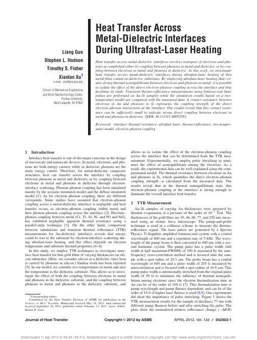
Liang Guo Stephen L.Hodson Timothy S.FisherXianfan Xu1e-mail:xxu@ School of Mechanical Engineering and Birck Nanotechnology Center,Purdue University,West Lafayette,IN47907Heat Transfer AcrossMetal-Dielectric Interfaces During Ultrafast-Laser Heating Heat transfer across metal-dielectric interfaces involves transport of electrons and pho-nons accomplished either by coupling between phonons in metal and dielectric or by cou-pling between electrons in metal and phonons in dielectric.In this work,we investigate heat transfer across metal-dielectric interfaces during ultrafast-laser heating of thin metalfilms coated on dielectric substrates.By employing ultrafast-laser heating that cre-ates strong thermal nonequilibrium between electrons and phonons in metal,it is possible to isolate the effect of the direct electron–phonon coupling across the interface and thus facilitate its study.Transient thermo-reflectance measurements using femtosecond laser pulses are performed on Au–Si samples while the simulation results based on a two-temperature model are compared with the measured data.A contact resistance between electrons in Au and phonons in Si represents the coupling strength of the direct electron–phonon interactions at the interface.Our results reveal that this contact resist-ance can be sufficiently small to indicate strong direct coupling between electrons in metal and phonons in dielectric.[DOI:10.1115/1.4005255]Keywords:interface thermal resistance,ultrafast laser,thermo-reflectance,two-temper-ature model,electron–phonon coupling1IntroductionInterface heat transfer is one of the major concerns in the design of microscale and nanoscale devices.In metal,electrons,and pho-nons are both energy carriers while in dielectric phonons are the main energy carrier.Therefore,for metal-dielectric composite structures,heat can transfer across the interface by coupling between phonons in metal and dielectric or by coupling between electrons in metal and phonons in dielectric through electron-interface scattering.Phonon–phonon coupling has been simulated mainly by the acoustic mismatch model and the diffuse mismatch model[1].As for electron–phonon coupling,there are different viewpoints.Some studies have assumed that electron–phonon coupling across a metal-dielectric interface is negligible and heat transfer occurs as electron–phonon coupling within metal and then phonon–phonon coupling across the interface[2].Electron–phonon coupling between metal(Cr,Ti,Al,Ni,and Pt)and SiO2 has exhibited negligible apparent thermal resistance using a parallel-strip technique[3].On the other hand,comparison between simulations and transient thermal reflectance(TTR) measurements for Au-dielectric interfaces reveals that energy could be lost to the substrate by electron-interface scattering dur-ing ultrafast-laser heating,and this effect depends on electron temperature and substrate thermal properties[4–6].In this study,we employ TTR techniques to investigate inter-face heat transfer for thin goldfilms of varying thicknesses on sili-con substrates.(Here,we consider silicon as a dielectric since heat is carried by phonons in silicon.)Similar work has been reported [5].In our model,we consider two temperatures in metal and also the temperature in the dielectric substrate.This allows us to inves-tigate the effect of both the coupling between electrons in metal and phonons in the dielectric substrate,and the coupling between phonons in metal and phonons in the dielectric substrate,and allows us to isolate the effect of the electron–phonon coupling across the interface that can be determined from the TTR mea-surement.Experimentally,we employ pulse stretching to mini-mize the effect of nonequilibrium among the electrons.As a result,the experimental data can be well-explained using the com-putational model.The thermal resistance between electrons in Au and phonons in Si,which quantifies the direct electron–phonon coupling strength,is calculated from the measured data.The results reveal that in the thermal nonequilibrium state,this electron–phonon coupling at the interface is strong enough to dominate the overall interface heat transfer.2TTR MeasurementAu–Si samples of varying Au thicknesses were prepared by thermal evaporation at a pressure of the order of10À7Torr.The thicknesses of the goldfilms are39,46,60,77,and250nm,meas-ured using an atomic force microscope.The pump-and-probe technique is used in a collinear scheme to measure the thermo-reflectance signal.The laser pulses are generated by a Spectra Physics Ti:Sapphire amplified femtosecond system with a central wavelength of800nm and a repetition rate of5kHz.The wave-length of the pump beam is then converted to400nm with a sec-ond harmonic crystal.The pump pulse has a pulse width(full width at half maximum-FWHM)of390fs measured by the sum-frequency cross-correlation method and is focused onto the sam-ple with a spot radius of20.3l m.The probe beam has a central wavelength of800nm and a pulse width of205fs measured by autocorrelation and is focused with a spot radius of16.9l m.This pump pulse width is intentionally stretched from the original pulse width of50fs to minimize the influence of thermal nonequili-brium among electrons since the electron thermalization time in Au can be of the order of100fs[7].This thermalization time is pump wavelength and pumpfluence dependent,and can be of the order of10fs if higher laserfluence is used[8,9].Our experiments did show the importance of pulse stretching.Figure1shows the TTR measurement results for the sample of thickness77nm with different pumpfluences before and after stretching the pulse.The plots show the normalized relative reflectance change(ÀD R/R)1Corresponding author.Contributed by the Heat Transfer Division of ASME for publication in the J OURNAL OF H EAT T RANSFER.Manuscript received May18,2011;final manuscript received September30,2011;published online February13,2012.Assoc.Editor: Robert D.Tzou.with the delay time between the pump and the probe pulses to show the contrast in cooling rates.With a shorter pulse (Fig.1(a )),a steep initial drop is seen in the signal,which is attributed to the behavior of nonequilibrium among electrons.Since the TTM to be used for simulation assumes a well-defined tempera-ture for electrons,i.e.,the electrons in gold have reached thermal equilibrium (not necessarily a uniform temperature),the model cannot predict the fast initial drop in the signals in Fig.1(a ).As will be shown later,the signals obtained by stretching the pulse can be predicted well using the TTM.3Two-Temperature Model for Thermal Reflectance MeasurementsUltrafast-laser heating induces thermal nonequilibrium between electrons and phonons in metal,which can be described by the TTM [10–13].We note that the heterogeneous interface consid-ered here involves three primary temperature variables (two in the metal and one in the dielectric).The “two-temperature”model is applied to the metal side.For investigating electron–phonon and phonon–phonon coupling at the interface,two thermal resistances are defined:R es (its reciprocal)indicates the coupling strength between electrons in metal and phonons in dielectric,while R ps indicates the coupling strength between phonons in metal and phonons in dielectric.(Large thermal resistance corresponds to weak coupling.)The resulting governing equations,initial,and interface conditions areC e @T e @t ¼k e @2T e@x2ÀG ðT e ÀT p ÞþS (1a )C p @T p @t ¼k p @2T p @x 2þG ðT e ÀT p Þ(1b )C s @T s @t ¼k s @2T s@x(1c )T e ðt ¼0Þ¼T p ðt ¼0Þ¼T s ðt ¼0Þ¼T 0(2)Àk e@T e @xx ¼L ¼T e ÀT s R es x ¼L(3a )Àk p @T px ¼L ¼T p ÀT s ps x ¼L(3b )Àk s@T sx ¼L ¼T e ÀT s es x ¼L þT p ÀT s ps x ¼L(3c )The subscripts e ,p ,and s denote electrons in metal,phonons in metal,and phonons in the dielectric substrate,respectively.C is the volumetric heat capacity,k is the thermal conductivity,G is the electron–phonon coupling factor governing the rate of energy transfer from electrons to phonons in metal,and L is the thickness of the metal layer.At the front surface of the metal layer insula-tion boundary condition is used due to the much larger heat flux caused by laser heating relative to the heat loss to air.At the rear surface of the substrate,since the thickness of the substrate used is large enough (1l m)so that there is no temperature rise during the time period of consideration,the insulation boundary condition is also applied.Thermal properties of phonons in both metal and dielectric are taken as temperature-independent due to the weak temperature dependence.The thermal conductivity of phonons in metal is much smaller than that of the electrons and is taken in this work as 0.001times the bulk thermal conductivity of gold (311W/(mK)).The volumetric heat capacity of the metal phonon is taken as that of the bulk gold.C e is taken as proportional to T e [14]with the proportion coefficient being 70J/(m 3K 2)[15],and k e is calculated by the model and the data used in Ref.[13]which is valid from the room temperature to the Fermi temperature (6.39Â104K in Au,[14]).G can be obtained using the model derived in Ref.[16].In this work,the value of G at the room tem-perature is taken as 4.6Â1016W/(m 3K)[17],and its dependence on electron and phonon temperatures follows [16].The laser heat-ing source term S is represented by the model used in [13]asS ¼0:94ð1ÀR ÞJ t p ðd þd b Þ1Àexp ÀL d þd bexp Àx d þd b À2:77t t p2"#(4)which assumes all the absorbed laser energy is deposited in the metal layer.J is the fluence of the pump laser,R is the surface re-flectance to the pump,t p is the pulse width (FWHM),d is the opti-cal penetration depth,and d b is the electron ballistic length (around 100nm in Au,[18]).R es and R ps are treated as free pa-rameters for fitting the experimental data.The wavelength of the probe laser in the experiment is centered at 800nm.For this wavelength,the incident photon energy is below the interband transition threshold in Au,which is around 2.47eV [18],and the Drude model can be used to relate the tem-peratures of electrons and phonons to the dielectric function and then the index of refraction,which is expressed as [19]e ¼e 1Àx 2px ðx þi x s Þ(5)x is the frequency of the probe laser and x p is the plasma fre-quency (1.37Â1016rad/s in Au evaluated using the data in Ref.[14]).x s is the electron collisional frequency,the inverse of the electron relaxation time.The temperature dependence ofelectricalFig.1TTR measurement results for the Au–Si sample of Authickness 77nm with different fluences.(a )Results before pulse stretching;(b )results after pulse stretching.resistivity indicates that x s is approximately proportional to pho-non temperature at high temperature [14]and from the Fermi liq-uid theory,its variation with electron temperature is quadratic (T e 2)[20].Therefore,x s is related to T e and T p approximately asx s ¼A ee T 2e þB ep T p(6)A ee is estimated from the low-temperature measurement [21]andB ep is usually estimated from the thermal or electrical resistivity near the room temperature [14].In this work,A ee is taken as the lit-erature value 1.2Â107s À1K À2[6]while e 1and B ep are evaluated by fitting the room-temperature value of the complex dielectric con-stant at 800nm wavelength provided in Ref.[22],which are found to be 9.7and 3.6Â1011s À1K À1,respectively.The complex index of refraction n 0þin 00is the square root of the dielectric ing Eqs.(5)and (6),n 0and n 00are evaluated as 0.16and 4.90,respectively,which agree with the empirical values [23].The re-flectance is then calculated from n 0and n 00by the method of transfer matrix [24],which considers multiple reflections in thin films.4Results and DiscussionThe results of TTR measurements with a pump fluence of 147J/m 2are plotted in Fig.2.The fast decrease of the reflectance indicates that energy transfer between electrons and phonons in metal,followed by a relatively slow decrease after several ps which indicates electrons and phonons have reached thermal equi-librium.The initial cooling rates are smaller for samples with thicknesses less than the electron ballistic length since the electron temperature is almost uniform across the thin film,and coupling with phonons within the metal film and the dielectric substrate is the only cooling mechanism.For a thicker sample of thickness 250nm,the initial decrease is much faster due to thermal diffu-sion in the gold film caused by a gradient of the electron tempera-ture in the film.We investigate the effect of R es and R ps using the thermo-reflectance signal.Two values of R ps ,1Â10À10m 2K/W and 1Â10À7m 2K/W,are used,each with a parameterized range of values for R es .Figure 3shows the calculated results for the sample with a 39nm-thick gold film.Little difference can be seen between Figs.3(a )and 3(b )while different cooling rates are obtained with varying R es in either plot,indicating that the cooling rate is not sensitive to the coupling strength between phonons in metal and dielectric.Note that an interface resistance of 1Â10À10m 2K/W is lower than any reported value,indicating a very high coupling strength between the phonons in metal and dielectric.Conversely,the results vary greatly with the coupling strength between electrons in metal and phonons in dielectric at the interface.This is because the lattice (phonon)temperature rise in metal is much smaller than the elec-tron temperature that the interface coupling between phonons in metal and dielectric does not influence the surface temperature,which directly determines the measured reflectance.On the other hand,the temperature rise of electrons is much higher,and conse-quently,the cooling rate is sensitive to R es .The relatively high sensitivity of R es to that of R ps demonstrates that the former can be isolated for the study of the coupling between electrons in metal and phonons in dielectric.We now use the measured TTR data to estimate R es ,the thermal resistance between electrons in metal and phonons in dielectric.R es is adjusted by the least square method to fit the simulation results with the measured data,and the results are shown in Fig.4.We note that it is impossible to fit the measured results using insu-lation interface condition (i.e.,no coupling or extremely large thermal resistance between electrons in metal and phonons in the dielectric substrate),which will significantly underestimate the cooling rate.For thin samples,we find that the value of R es is of the order of 10À10to 10À9m 2K/W.This value is below the ther-mal resistances of representative solid–solid interfaces measured in thermal equilibrium [25].This indicates that the direct coupling between electrons in metal and phonons in dielectric is strong.It is also noted that the resistance values increases with the thickness of the gold film,indicating a decrease in the coupling strength between electrons in metal and the dielectric substrate.This could be due to the lower electron temperature obtained in thicker films,and a decrease of the coupling strength with a decrease in the electron temperature [5].For the sample of thickness 250nm,R es has little effect on the simulation result since the interface is too far from the absorbing surface to influence the surface tempera-ture,and therefore it is not presented here.The agreement between the fitted results and the measured data is generally good.The small discrepancy between the measured and the fitted results can result from inaccuracy in computingtheFig.2TTR measurement results on Au–Si samples of varying AuthicknessesFig.3Simulation results with varying R es for the Au–Si sample of Au thickness 39nm.(a )R ps 51310210m 2K/W;(b )R ps 5131027m 2K/W.absorption or the temperature.Figure 1(b)shows the normalized TTR measurement results on the sample of thickness 77nm with three laser fluences.It is seen that small variations in the shape of the TTR signals can be caused by different laser fluences and thus the maximum temperature reached in the film.Absorption in metal,multiple reflections between the metal surface and the Au–Si inter-face,and possible deviations of the properties of thin films from those of bulk can all contribute to uncertainties in the temperature simulation;therefore affecting the calculated reflectance.With the values of R es shown in Fig.4,the calculation shows that the highest electron temperature,which is at the surface of 39nm–thick gold film,is about 6700K.The highest temperature of electrons is roughly inversely proportional to the thickness of the films for the four thinner films.The highest temperature of elec-trons is much less than the Fermi temperature and thus ensures the validity of the linear dependence of C e on T e [14].The highest temperature for the lattice in metal is about 780K,also in the 39nm-thick gold film.This large temperature difference between electrons and lattice indicates that the interface heat transfer is dominated by the coupling between electrons in metal and the phonons in the dielectric substrate.As shown in Fig.4,the meas-ured R es is very low,of the order of 10À10to 10À9m 2K/W.Even if R ps ,which is not determined in this study,is also that low (note that 10À10to 10À9m 2K/W is lower than any reported values),because of the large difference in temperatures between electrons and the phonons in metal,the interface heat transfer rate (Eqs.(3a )–(3c ))due to the coupling between electrons in metal and the substrate is much larger than that due to the coupling between phonons in metal and the substrate.5ConclusionsIn conclusion,TTR measurements using femtosecond laser pulses are performed on Au–Si samples and the results are analyzed using the TTM model.It is shown that due to the strong nonequilibrium between electrons and phonons during ultrafast-laser heating,it is possible to isolate the effect of the direct electron–phonon coupling across the interface,allowing investiga-tion of its ing stretched femtosecond pulses is shown to be able to minimize the nonequilibrium effect among electrons,and is thus more suitable for this study.The TTR measurement data can be well-represented using the TTM parison between the TTR data and the TTM results indicates that the direct coupling due to electron-interface scattering dominates the interface heat transfer during ultrafast-laser heating of thin films.AcknowledgmentThis paper is based upon work supported by the Defense Advanced Research Projects Agency and SPAWAR Systems Cen-ter,Pacific under Contract No.N66001-09-C-2013.The authors also thank C.Liebig,Y.Wang,and W.Wu for helpful discussions.NomenclatureA ee ¼coefficient in Eq.(6),s À1K À2B ep ¼coefficient in Eq.(6),s À1K À1C ¼volumetric heat capacity,J/(m 3K)G ¼electron–phonon coupling factor,W/(m 3K)i ¼unit of the imaginary number J ¼fluence of the pump,J/m 2k ¼thermal conductivity,W/(mK)L ¼metal film thickness,mn 0¼real part of the complex index of refractionn 00¼imaginary part of the complex index of refraction R ¼interface thermal resistance,m 2K/W;reflectance S ¼laser source term,W/m3Fig.4Comparison between the measurement and the simulation results for Au–Si samples of different Au thicknesses.The open circle represents the meas-ured data and the solid line represents the simulation results.(a )39nm fitted by R es 55310210m 2K/W;(b )46nm fitted by R es 56310210m 2K/W;(c )60nm fitted by R es 51.231029m 2K/W;and (d )77nm fitted by R es 51.831029m 2K/W.T¼temperature,Kt¼time,st p¼pulse width of the pump(FWHM),sx¼spatial coordinate,me¼complex dielectric constante1¼constant in the Drude modeld¼radiation penetration depth,md b¼electron ballistic depth,mx¼angular frequency of the probe,rad/sx p¼plasma frequency,rad/sx s¼electron collisional frequency,rad/sSubscripts0¼initial statee¼electron in metales¼electron in metal and phonon in dielectricp¼phonon in metalps¼phonon in metal and phonon in dielectrics¼phonon in dielectricReferences[1]Cahill,D.G.,Ford,W.K.,Goodson,K.E.,Mahan,G.D.,Majumdar,A.,Maris,H.J.,Merlin,R.,and Phillpot,S.R.,2003,“Nanoscale Thermal Trans-port,”J.Appl.Phys.,93(2),pp.793–818.[2]Majumdar,A.,and Reddy,P.,2004,“Role of Electron–Phonon Coupling inThermal Conductance of Metal–Nonmetal Interfaces,”Appl.Phys.Lett., 84(23),pp.4768–4770.[3]Chien,H.-C.,Yao,D.-J.,and Hsu,C.-T.,2008,“Measurement and Evaluationof the Interfacial Thermal Resistance Between a Metal and a Dielectric,”Appl.Phys.Lett.,93(23),p.231910.[4]Hopkins,P.E.,and Norris,P.M.,2007,“Substrate Influence in Electron–Phonon Coupling Measurements in Thin Au Films,”Appl.Surf.Sci.,253(15), pp.6289–6294.[5]Hopkins,P.E.,Kassebaum,J.L.,and Norris,P.M.,2009,“Effects of ElectronScattering at Metal–Nonmetal Interfaces on Electron-Phonon Equilibration in Gold Films,”J.Appl.Phys.,105(2),p.023710.[6]Hopkins,P.E.,2010,“Influence of Electron-Boundary Scattering on Thermore-flectance Calculations After Intraband and Interband Transitions Induced by Short-Pulsed Laser Absorption,”Phys.Rev.B,81(3),p.035413.[7]Sun,C.-K.,Vallee,F.,Acioli,L.,Ippen,E.P.,and Fujimoto,J.G.,1993,“Femtosecond Investigation of Electron Thermalization in Gold,”Phys.Rev.B, 48(16),pp.12365–12368.[8]Fann,W.S.,Storz,R.,Tom,H.W.K.,and Bokor,J.,1992,“Electron Thermal-ization of Gold,”Phys.Rev.B,46(20),pp.13592–13595.[9]Fann,W.S.,Storz,R.,Tom,H.W.K.,and Bokor,J.,1992,“Direct Measure-ment of Nonequilibrium Electron-Energy Distributions in Subpicosecond Laser-Heated Gold Films,”Phys.Rev.Lett.,68(18),pp.2834–2837.[10]Kaganov,M.I.,Lifshitz,I.M.,and Tanatarov,L.V.,1957,“RelaxationBetween Electrons and the Crystalline Lattice,”Sov.Phys.JETP,4(2),pp.173–178.[11]Anisimov.S.I.,Kapeliovich,B.L.,and Perel’man,T.L.,1974,“ElectronEmission From Metal Surfaces Exposed to Ultrashort Laser Pulses,”Sov.Phys.JETP,39(2),pp.375–377.[12]Qiu,T.Q.,and Tien,C.L.,1993,“Heat Transfer Mechanisms During Short-Pulse Laser Heating of Metals,”ASME Trans.J.Heat Transfer,115(4),pp.835–841.[13]Chowdhury,I.H.,and Xu,X.,2003,“Heat Transfer in Femtosecond LaserProcessing of Metal,”Numer.Heat Transfer,Part A,44(3),pp.219–232. [14]Kittel,C.,1976,Introduction to Solid State Physics,John Wiley&Sons,Inc.,New York.[15]Smith,A.N.,and Norris,P.M.,2001,“Influence of Intraband Transitions onthe Electron Thermoreflectance Response of Metals,”Appl.Phys.Lett.,78(9), pp.1240–1242.[16]Chen,J.K.,Latham,W.P.,and Beraun,J.E.,2005,“The Role of Electron–Phonon Coupling in Ultrafast Laser Heating,”ser Appl.,17(1),pp.63–68.[17]Hostetler,J.L.,Smith,A.N.,Czajkowsky,D.M.,and Norris,P.M.,1999,“Measurement of the Electron-Phonon Coupling Factor Dependence on Film Thickness and Grain Size in Au,Cr,and Al,”Applied Optics,38(16),pp.3614–3620.[18]Hohlfeld,J.,Wellershoff,S.-S.,Gudde,J.,Conrad,U.,Jahnke,V.,and Mat-thias,E.,2000,“Electron and Lattice Dynamics Following Optical Excitation of Metals,”Chem.Phys.,251(1–3),pp.237–258.[19]Maier,S.A.,2007,Plasmonics:Fundamentals and Applications,SpringerScienceþBusiness Media,New York.[20]Ashcroft,N.W.,and Mermin,N.D.,(1976),Solid State Physics,W.B.Saun-ders,Philadelphia.[21]MacDonald,A.H.,1980,“Electron-Phonon Enhancement of Electron-ElectronScattering in Al,”Phys.Rev.Lett.,44(7),pp.489–493.[22]Johnson,P.B.,and Christy,R.W.,1972,“Optical Constants of the Noble Met-als,”Phys.Rev.B,6(12),pp.4370–4379.[23]Palik,E.D.,(1998),Handbook of Optical Constants of Solids,Academic,SanDiego.[24]Pedrotti,F.L.,Pedrotti,L.S.,and Pedrotti,L.M.,(2007),Introduction toOptics,Pearson Prentice Hall,Upper Saddle River,NJ.[25]Incropera,F.P.,Dewitt,D.P.,Bergman,T.L.,and Lavine,A.S.,2007,Funda-mentals of Heat and Mass Transfer,John Wiley&Sons,Inc.,Hoboken,NJ.。
伊朗法尔斯地区第三系砂岩的古地磁

a,
Dominique
Frizon de Lamotte b
a ~
' , C h a r l e s A u b o u r g a,
Jamshid Hassanzadeh
" Universitg de Cergy-Pontoise, Dept. des Sciences de la Terre (CNRS, URAI759), F95011, Cergy-Pontoise Cedex, France I~Institute of Geophysics, Tehran UniversiO, PO. Box 14155-6466, Tehran, lran
Keywords: fold-thrust belt; magnetic fabric; sandstone; weak deformation; Arc of Fars; Zagros (Iran)
1. I n t r o d u c t i o n In sedimentary rocks undergoing horizontal shortening, the initial sedimentary fabric is progressively erased and replaced by a tectonic one (Ramsay and Huber, 1983). The analysis of these initial stages of deformation during which the inherited sedimentary fabric and the tectonic fabric interact, is generally not well documented due to the subtlety of the ini-
里德堡原子微波电场测量

doi:10.11823/j.issn.1674-5795.2021.01.01里德堡原子微波电场测量白金海,胡栋,贡昊,王宇(航空工业北京长城计量测试技术研究所,北京100095)摘要:里德堡原子是处于高激发态的原子,其主量子数大、寿命高,具有极化率高、电偶极矩大等特点,对外电场十分敏感。
基于热蒸气室中里德堡原子的量子干涉原理(电磁感应透明和Autler-Towns分裂效应)的微波电场精密测量不仅具有远高于传统偶极天线的灵敏度,且具有自校准、对外电场干扰少、测量频率范围大等优点,是下一代电场测量标准。
本文综述了里德堡原子的微波电场测量研究,详细介绍了其基本原理和当前研究进展,并讨论了未来发展方向。
关键词:量子精密测量;里德堡原子;微波电场;电磁感应透明中图分类号:TB97文献标识码:A文章编号:1674-5795(2021)01-0001-09Rydberg Atoms Based Microwave Electric Field SensingBAIJinhai,HU Dong,GONG Hao$WANG Yu(Changcheng Institute of Metrology&Measurement,Beijing100095,China)Abstract:Rydberg atoms are the atoms in highly excited states with lar-e principaO quantum numbers n,and long lifetimes.The lar-e Ryd-ber-atom polarizabilitu and strong dipole transitions between enereetically nearby states are highly sensitive to electris fielOs.The new developed scheme for microwave electric field precision measurement is based on quantum interference effects(electromaaneticclly induced transparency and Autler-Townes splitting)in Rydbere atoms contained in a dielectric vapoe cell.The mininium measured strengths of microwave electric fieies of the new scheme are far below the standard values obtained by traditional antenna methods.And it has several advantages,such as self-calibration,non-perturbation to the measured field,a broadband measurement frequency range,etc,is the next-generation electric field standard.In this review,we describe work on the new method for measuring microwave electric field based on Rydberg atoms.We introducc the basic theory and experimental techniques of the new method,and discuss the future development direction.Key words:quantum precision measurement;Rydberg atoms;microwave electric fielO;electromagnetically induced transparency0引言原子是一种典型的量子体系,具有可复现、性能稳定、能级精确等优点。
压电材料的研究新进展

压电材料的研究新进展温建强;章力旺【摘要】压电材料作为机电转换的功能材料,在高新技术领域扮演着重要的角色.锆钛酸铅压电陶瓷凭借其优良的性能,自投入使用以来成为最广泛使用的压电材料.近年来,探索和发展潜在的替代新型材料备受重视.本文就近些年来国内外压电材料技术研究进展中呈现的无铅化、高性能化、薄膜化的新趋势进行了综述,并对今后的研究提出一些发展性的建议.【期刊名称】《应用声学》【年(卷),期】2013(032)005【总页数】6页(P413-418)【关键词】压电材料;压电性能;无铅压电材料;压电薄膜【作者】温建强;章力旺【作者单位】中国科学院声学研究所北京100190;中国科学院声学研究所北京100190【正文语种】中文【中图分类】TM2821 引言1880年P.Curie和J.Curie首次发现石英晶体有压电效应,1954年美国 B.Jaffe 发现了锆钛酸铅(PZT)压电陶瓷,此后逐渐发展为国内外主流的压电材料,在功能材料领域占有重要的地位[1]。
压电材料发展的类型主要有单晶、多晶、微晶玻璃、有机高分子、复合材料等。
20世纪80年代以来,随着压电陶瓷材料从二元系向三元、多元系的开发研究高潮的结束,压电材料的研究一度进展缓慢。
随着科学技术快速发展,应用需求牵引下的开发探索给予了压电材料研究的新动力,加上科技工作者在基础性研究和生产工艺改进上的不懈努力,近十几年来,新型的压电材料不断涌现出,并呈现出无铅化、高性能化、薄膜化的态势,使得压电材料研究的面貌焕然一新,带动相应的应用器件研究也日趋活跃。
本文就近些年来国内外压电材料技术研究中所呈现出的新趋势和最新进展进行介绍,并对今后研究的努力发展方向进行展望,并提出一些建议。
2 压电材料研究的新趋势2.1 无铅化随着环境保护和社会可持续发展的要求,发展环境协调性材料及技术已是公认的大势所趋。
为了防止环境污染,国内外科研人员对无铅压电材料开展了大量的研究工作并取得了令人鼓舞的进展[2]。
太赫兹波段超材料的制作、设计及应用
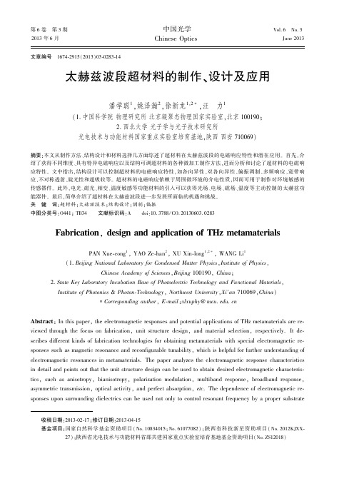
第6卷 第3期2013年6月 中国光学 Chinese Optics Vol.6 No.3June 2013 收稿日期:2013⁃02⁃17;修订日期:2013⁃04⁃15 基金项目:国家自然科学基金资助项目(No.10834015;No.61077082);陕西省科技新星资助项目(No.2012KJXX⁃27);陕西省光电技术与功能材料省部共建国家重点实验室培育基地基金资助项目(No.ZS12018)文章编号 1674⁃2915(2013)03⁃0283⁃14太赫兹波段超材料的制作、设计及应用潘学聪1,姚泽瀚2,徐新龙1,2∗,汪 力1(1.中国科学院物理研究所北京凝聚态物理国家实验室,北京100190;2.西北大学光子学与光子技术研究所光电技术与功能材料国家重点实验室培育基地,陕西西安710069)摘要:本文从制作方法、结构设计和材料选择几方面综述了超材料在太赫兹波段的电磁响应特性和潜在应用。
首先,介绍了获得不同维度、具有特异电磁响应以及结构可调超材料的各种微加工制作方法,进而分析和讨论了超材料的电磁响应特性。
文中指出,结构设计可以控制超材料的电磁响应特性,如各向异性、双各向异性、偏振调制、多频响应、宽带响应、不对称透射、旋光性和超吸收等。
超材料的电磁响应依赖于周围微环境的介电性质,因而可用于制作对环境敏感的传感器件。
此外,电光、磁光、相变、温度敏感等功能材料的引入可以获得光场、电场、磁场、温度等主动控制的太赫兹功能器件。
最后,简单介绍了超材料在太赫兹波段进一步发展所面临的机遇和挑战。
关 键 词:超材料;太赫兹技术;结构设计;调制;偏振中图分类号:O441;TB34 文献标识码:A doi:10.3788/CO.20130603.0283Fabrication ,design and application of THz metamaterialsPAN Xue⁃cong 1,YAO Ze⁃han 2,XU Xin⁃long 1,2∗,WANG Li 1(1.Beijing National Laboratory for Condensed Matter Physics ,Institute of Physics ,Chinese Academy of Sciences ,Beijing 100190,China ;2.State Key Laboratory Incubation Base of Photoelectric Technology and Functional Materials ,Institute of Photonics &Photon⁃Technology ,Northwest University ,Xi′an 710069,China )∗Corresponding author ,E⁃mail :xlxuphy@ Abstract :In this paper,the electromagnetic responses and potential applications of THz metamaterials are re⁃viewed through the focus on fabrication,unit structure design,and material selection,respectively.It de⁃scribes different kinds of fabrication technologies for obtaining metamaterials with special electromagnetic re⁃sponses such as magnetic resonance and reconfigurable tunability,which is helpful for further understanding of electromagnetic resonances in metamaterials.The paper analyzes the electromagnetic response characteristics in detail and points out that the unit structure design can be used to obtain desired electromagnetic characteris⁃tics,such as anisotropy,bianisotropy,polarization modulation,multiband response,broadband response,asymmetric transmission,optical activity,and perfect absorption,etc .The dependence of electromagnetic re⁃sponses upon surrounding dielectrics can be used not only to control resonant frequency by a proper substrateselection,but also for sensing applications.Furthermore,the introduction of functional materials with control⁃lable dielectric properties by external optical field,electrical field,magnetic field and temperature has the po⁃tential to achieve tunable metamaterials,which is highly desirable for THz functional devices.Finally,the op⁃portunities and challenges for further developments of THz metamaterials are briefly introduced.Key words:metamaterials;THz technology;structure design;modulation;polarization1 引 言 通过对自然材料的裁剪、加工和设计,从而实现对电子、光子以及其他一些元激发准粒子的人为调控,一直是光电科学研究的重点。
advanced optical materials分区
Advanced Optical MaterialsIntroductionAdvanced optical materials are a class of materials that possess unique optical properties and are engineered to enhance light-matter interactions. These materials have revolutionized various fields such as photonics, optoelectronics, and nanotechnology. In this article, we will explore the different types of advanced optical materials, their applications, and the future prospects of this exciting field.Types of Advanced Optical MaterialsPhotonic CrystalsPhotonic crystals are periodic structures that can manipulate the propagation of light. They consist of a periodic arrangement ofdielectric or metallic components with alternating refractive indices. These structures can control the flow of light by creating energy bandgaps, which prohibit certain wavelengths from propagating through the material. Photonic crystals find applications in optical communication, sensing, and solar cells.MetamaterialsMetamaterials are artificially engineered materials that exhibit properties not found in nature. They are composed of subwavelength-sized building blocks arranged in a periodic or random manner. Metamaterials can manipulate electromagnetic waves by achieving negative refractive index, perfect absorption, and cloaking effects. These unique properties have led to applications in invisibility cloaks, super lenses, and efficient light harvesting.Plasmonic MaterialsPlasmonic materials exploit the interaction between light and free electrons at metal-dielectric interfaces to confine light at nanoscale dimensions. This confinement results in enhanced electromagnetic fields known as surface plasmon resonances. Plasmonic materials have diverse applications such as biosensing, photothermal therapy, and enhanced solar cells.Quantum DotsQuantum dots are nanoscale semiconductor crystals with unique optical properties due to quantum confinement effects. Their size-tunable bandgap enables them to emit different colors of light depending ontheir size. Quantum dots find applications in display technologies (e.g., QLED TVs), biological imaging, and photovoltaics.Organic Optoelectronic MaterialsOrganic optoelectronic materials are based on organic compounds that exhibit electrical conductivity and optical properties. These materials are lightweight, flexible, and can be processed at low cost. They find applications in organic light-emitting diodes (OLEDs), organic photovoltaics (OPVs), and organic field-effect transistors (OFETs).Applications of Advanced Optical MaterialsInformation TechnologyAdvanced optical materials play a crucial role in information technology. Photonic crystals enable the miniaturization of optical devices, leading to faster and more efficient data transmission. Metamaterials offer possibilities for creating ultra-compact photonic integrated circuits. Plasmonic materials enable the development of high-density data storage devices.Energy HarvestingAdvanced optical materials have revolutionized energy harvesting technologies. Quantum dots and organic optoelectronic materials are used in next-generation solar cells to enhance light absorption and efficiency. Plasmonic nanoparticles can concentrate light in solar cells, increasing their power output. These advancements contribute to the development of sustainable energy sources.Sensing and ImagingThe unique optical properties of advanced optical materials make them ideal for sensing and imaging applications. Quantum dots are used as fluorescent probes in biological imaging due to their bright emissionand excellent photostability. Metamaterial-based sensors offer high sensitivity for detecting minute changes in refractive index ormolecular interactions.Biomedical ApplicationsAdvanced optical materials have significant implications in biomedical research and healthcare. Plasmonic nanomaterials enable targeted drug delivery, photothermal therapy, and bioimaging with high spatial resolution. Organic optoelectronic materials find applications in wearable biosensors, smart bandages, and flexible medical devices.Future ProspectsThe field of advanced optical materials is rapidly evolving with continuous advancements being made in material synthesis, characterization techniques, and device fabrication processes. Thefuture prospects of this field are promising, with potential breakthroughs in areas such as:1.Quantum Optics: Integration of advanced optical materials withquantum technologies could lead to the development of quantumcomputers, secure communication networks, and ultra-precisesensors.2.Flexible and Wearable Electronics: Organic optoelectronicmaterials offer the potential for flexible and wearable electronic devices, such as flexible displays, electronic textiles, andimplantable medical devices.3.Optical Computing: Photonic crystals and metamaterials may pavethe way for all-optical computing, where photons replace electrons for faster and more energy-efficient data processing.4.Enhanced Optoelectronic Devices: Continued research on advancedoptical materials will lead to improved performance and efficiency of optoelectronic devices such as solar cells, LEDs, lasers, andphotodetectors.In conclusion, advanced optical materials have opened up newpossibilities in various fields by enabling unprecedented control over light-matter interactions. The ongoing research and development in this field promise exciting advancements in information technology, energy harvesting, sensing and imaging, as well as biomedical applications. The future looks bright for advanced optical materials as they continue to revolutionize technology and shape our world.。
泰山医学院材料导论题库
泰山医学院《材料导论》试题库1、The nucleus of an atom containsA ProtonsB ElectronsC NeutronsD All of the abovev E Both A and C2、What type(s) of electron subshell(s) does an L shell contain?A a p f sB s and fv C s and p3、What is the maximum number of electrons that an M shell may contain?v A.18B.32C.84、Match the electron structure below with the element type it represents.1s22s22p63s23p63d104s1A. Inert gasB. HalogenC. Alkali metalD. Alkaline earth metalv E. Transition metal5、What is the predominant type of bonding for titanium (Ti)?A. IonicB. HydrogenC. CovalentD. van der Waalsv E. Metallic6、Of those elements in the list situated below the periodic table, select the one that is one electron short of having its outer shell of electrons completely filled.v A. IB. NC. SD. SrE. Ar7、Which of the following materials may form crystalline solids?A. PolymersB. MetalsC. Ceramicsv D. All of the above8、Which of the following are the most common coordination numbers for ceramic materials?A. 2B. 3 and 6C. 4 and 12v D. 4,6 and 89、Which crystal system(s) listed below has (have) the following relationship for the unit cell edge lengths?a =b ≠cA. CubicB. HexagonalC. TriclinicD. MonoclinicE. RhombohedralF. OrthorhombicG. Tetragonalv H. Both C and E10、Which crystal system(s) listed below has (have) the following interaxial angle relationship? α= β = γ = 90°v A. CubicB. HexagonalC. TriclinicD. MonoclinicE. RhombohedralF. OrthorhombicG. Both A and D11、把a、b、c、d四块金属片浸入稀硫酸中,用导线两两相连组成原电池。
Effect of alloying elements on the microstructure and mechanical properties of nanostructured
LetterEffect of alloying elements on the microstructure and mechanical properties of nanostructured ferritic steels produced by spark plasmasinteringSomayeh Pasebani,Indrajit Charit ⇑Department of Chemical and Materials Engineering,University of Idaho,Moscow,ID 83844,USAa r t i c l e i n f o Article history:Received 23November 2013Received in revised form 23January 2014Accepted 29January 2014Available online 15February 2014Keywords:NanostructuresMechanical alloying Powder metallurgyTransmission electron microscopy High temperature alloya b s t r a c tSeveral Fe–14Cr based alloys with varying compositions were processed using a combined route of mechanical alloying and spark plasma sintering.Microstructural characteristics of the consolidated alloys were examined via transmission electron microscopy and atom probe tomography,and mechanical prop-erties evaluated using microhardness nthanum oxide (0.5wt.%)was added to Fe–14Cr leading to improvement in microstructural stability and mechanical properties mainly due to a high number den-sity of La–Cr–O-enriched nanoclusters.The combined addition of La,Ti (1wt.%)and Mo (0.3wt.%)to the Fe–14Cr base composition further enhanced the microstructural stability and mechanical properties.Nanoclusters enriched in Cr–Ti–La–O with a number density of 1.4Â1024m À3were found in this alloy with a bimodal grain size distribution.After adding Y 2O 3(0.3wt.%)along with Ti and Mo to the Fe–14Cr matrix,a high number density (1.5Â1024m À3)of Cr–Ti–Y–O-enriched NCs was also detected.For-mation mechanism of these nanoclusters can be explained through the concentrations and diffusion rates of the initial oxide species formed during the milling process and initial stages of sintering as well as the thermodynamic nucleation barrier and their enthalpy of formation.Ó2014Elsevier B.V.All rights reserved.1.IntroductionNanostructured ferritic steels (NFSs),a subcategory of oxide dis-persion strengthened (ODS)steels,have outstanding high temper-ature strength,creep strength [1,2]and excellent radiation damage resistance [3].These enhanced properties of NFSs have been attrib-uted to the high number density of Y–Ti–O-enriched nanoclusters (NCs)with diameter of 1–2nm [4].The Y–Ti–O-enriched NCs have been found to be stable under irradiation and effective in trapping helium [5].These NCs are formed due to the mechanical alloying (MA)of Fe–Cr–Ti powder with Y 2O 3during high energy ball milling followed by hot consolidation route such as hot isostatic pressing (HIP)or hot extrusion [6–8].Alinger et al.[4]have investigated the effect of alloying elements on the formation mechanism of NCs in NFSs processed by hot isostatic pressing (HIP)and reported both Ti and high milling energy were necessary for the formation of ler and Parish [9]suggested that the excellent creep properties in yttria-bearing NFSs result from the pinning of thegrain boundaries by a combined effect of solute segregation and precipitation.Although HIP and hot extrusion are commonly used to consoli-date the NFSs,anisotropic properties and processing costs are con-sidered challenging issues.Recently,spark plasma sintering (SPS)has been utilized to sinter the powder at a higher heating rate,low-er temperature and shorter dwell time.This can be done by apply-ing a uniaxial pressure and direct current pulses simultaneously to a powder sample contained in a graphite die [10].Except for a few studies on consolidation of simple systems such as Fe–9Cr–0.3/0.6Y 2O 3[11]and Fe–14Cr–0.3Y 2O 3[10],the SPS process has not been extensively utilized to consolidate the NFSs with complex compositions.Recently,the role of Ti and Y 2O 3in processing of Fe–16Cr–3Al–1Ti–0.5Y 2O 3(wt.%)via MA and SPS was investigated by Allahar et al.[12].A bimodal grain size distribution in conjunc-tion with Y–Ti–O-enriched NCs were obtained [12,13].In this study,Fe–14Cr (wt.%)was designed as the base or matrix alloy,and then Ti,La 2O 3and Mo were sequentially added to the ferritic matrix and ball milled.This approach allowed us to study the effect of individual and combined addition of solutes on the formation of NCs along with other microstructural evolutions.Furthermore,SPS instead of other traditional consolidation methods was used to consolidate the NFS powder.The mixture/10.1016/j.jallcom.2014.01.2430925-8388/Ó2014Elsevier B.V.All rights reserved.⇑Corresponding author.Tel.:+12088855964;fax:+12088857462.E-mail address:icharit@ (I.Charit).of Fe–Cr–Ti–Mo powder with Y2O3was also processed and characterized in a similar manner for comparison with the rest of the developed alloys.2.ExperimentalThe chemical compositions of all the developed alloys along with their identi-fying names in this study are given in Table1.High energy ball milling was per-formed in a SPEX8000M shaker mill for10h using Ar atmosphere with the milling media as steel balls of8mm in diameter and a ball to powder ratio(BPR) of10:1.A Dr.Sinter Lab SPS-515S was used to consolidate the as-milled powder at different temperatures(850,950and1050°C)for7min using the pulse pattern 12–2ms,a heating rate of100°C/min and a pressure of80MPa.The SPSed samples were in the form of disks with8mm in height and12mm in diameter.The density of the sintered specimens was measured by Archimedes’method. Vickers microhardness tests were performed using a Leco LM100microhardness tester operated at a load of1000g–f(9.8N).A Fischione Model110Twin-Jet Elec-tropolisher containing a mixture of CH3OH–HNO3(80:20by vol.%)as the electrolyte and operated at aboutÀ40°C was used to prepare specimens for transmission elec-tron microscopy(TEM).A FEI Tecnai TF30–FEG STEM operating at300kV was used. The energy dispersive spectroscopy(EDS)attached with the STEM was used to roughly examine the chemical composition of the particles.A Quanta3D FEG instrument with a Ga-ion source focused ion beam(FIB)was used to prepare spec-imens for atom probe tomography(APT)studies on14L,14LMT and14YMT sam-ples.The APT analysis was carried out using a CAMECA LEAP4000X HR instrument operating in the voltage mode at50–60K and20%of the standing volt-age pulse fraction.The atom maps were reconstructed using CAMECA IVAS3.6soft-ware and the maximum separation algorithm to estimate the size and chemical composition of NCs.This was applied to APT datasets each containing20–30million ions for each specimen.Lower evaporationfield of the nanoparticles and trajectory aberrations caused estimation of higher Fe atoms in the nanoclusters.Although the contribution of Fe atoms from the matrix was examined here,the matrix-correction was not addressed in this study.3.Results and discussionThe TEM brightfield micrographs for the various alloys SPSed at 950°C for7min are illustrated in Fig.1a–d.The microstructure of 14Cr alloy shown in Fig.1a revealed a complex microstructure with submicron subgrain-like structures,relatively high density of dislocations and low number density of oxide nanoparticles. The nanoparticles were larger(25–65nm)than the other SPSed al-loys and found to have chemical compositions close to Cr2O3and FeCr2O4as analyzed by energy dispersive spectroscopy.The microstructure of the consolidated14L alloy is shown in Fig.1b.The microstructure consisted of more ultrafine grains (<1l m but>100nm),a few nanograins with sharp boundaries and a higher number of nanoparticles mainly in the grain interiors. The number density of nanoparticles was higher than that of14Cr alloy shown in Fig.1a but lower than14LMT(Fig.1c)and14YMT (Fig.1d).In14L alloy,the nanoparticles with2–11nm in diameter were found inside the grains(hard to be observed at magnification given in Fig.1b and micrographs taken at higher magnifications was used for this purpose)whereas the nanoparticles with 50–80nm in diameter were located at the grain boundary regions. The particles on the boundaries are likely to be mainly Cr2O3and LaCrO3,but the chemical analysis of those smallest particles could not be done precisely due to the significant influence of the ferritic matrix.Fig.1c shows the microstructure of the SPSed14LMT alloy, consisting of both ultrafine grains(as defined previously)and nanograins(6100nm).The nanoparticles present in the micro-structure were complex oxides of Fe,Cr and Ti.The nanoparticles with faceted morphology and smaller than10nm in diameter were enriched in La and Ti.No evidence of stoichiometric La2TiO5or La2Ti2O7particles was observed based on the EDS and diffraction data.A similar type of microstructure was revealed in the SPSed 14YMT alloy as shown in Fig.1d.The particle size distribution histograms of the14Cr,14L, 14LMT and14YMT alloys are plotted in Fig.2a–d,respectively. Approximately1000particles were sampled from each alloy to de-velop the histograms.The average particle size decreased in order of14Cr,14L,14LMT and14YMT.The highest fraction of the particle size as shown in the histograms of14Cr,14L,14LMT and14YMT was found to be associated with25±5nm(18±2.5%),10±5nm (28±3%),5±1nm(40±6%)and5±1nm(46±5%)in diameter, respectively.The number density of nanoparticles smaller than 5±1nm was higher in14YMT than14LMT alloy.The3-D APT maps for14L alloy revealed a number density (%3Â1022mÀ3)of CrO–La–O-enriched NCs.The average Guinier radius of these NCs was1.9±0.6nm.The average composition of the NCs in14L was estimated by using the maximum separation algorithm to be Fe–17.87±3.4Cr–32.61±3.2O–8.21±1.1La(at.%).A higher number density(%1.4Â1024mÀ3)and smaller NCs with average Guinier radius of 1.43±0.20nm were observed in the APT maps for14LMT alloy as shown in Fig.3a.The NCs were Cr–Ti–La–O-enriched with the average composition of Fe–10.9±2.8Cr–30.9±3.1O–17.3±2.5Ti–8.2±2.2La(at.%).According to the LEAP measurements,the chemical composition of NCs dif-fered considerably from stoichiometric oxides.A large amount of Fe and Cr was detected inside the NCs,and La/Ti and La/O ratios were not consistent with La2TiO5or La2Ti2O7as expected based on thermodynamic calculations,rather the ratios were sub-stoichi-ometric.The3-D APT maps for14YMT alloy were similar to14YMT alloy as shown in Fig.3b.The NCs with an average radius of 1.24±0.2nm and a number density of1.5Â1024mÀ3were Cr–Ti–Y–O-enriched.The chemical composition of NCs was estimated close to Fe–8.52±3.1Cr–37.39±4.5O–24.52±3.1Ti–10.95±3.1Y (at.%).The matrix-corrected compositions are currently being ana-lyzed and will be reported in a full-length publication in near future.The relative density of various alloys sintered at850–1050°C is shown in Fig.4a.Generally,a higher density was obtained in the specimens sintered at higher temperatures.At850and950°C, the density of unmilled14Cr specimen(97.2%and97.5%)was higher than the milled/SPSed14Cr(92.8%and95.5%)because the unmilled powder particles were less hard(due to absence of strain hardening)and plastically deformed to a higher degree than the milled powder leading to a higher density.Adding0.5and 0.7wt.%of La2O3and0.3wt.%Y2O3to the14Cr matrix significantly decreased the density of the specimen,especially at850and 950°C;however,adding Ti to14L and14Y improved the density to some extent.The microhardness data of various alloys processed at different temperatures are shown in Fig.4b.In general,microhardness in-creased with increasing SPS temperatures up to950°C and then decreased.Both Y and La increased the hardness due to the disper-sion hardening effect.The hardness increased at the higher content of La due to the greater effect of dispersion hardening.Adding Ti separately to the14Cr matrix improved the hardness due to theTable1The alloy compositions and processing conditions(milled for10h and SPSed at850-1050°C for7min).Alloy ID Elements(wt.%)Cr Ti La2O3Y2O3Mo Fe14Cr-unmilled140000Bal.14Cr140000Bal.14T141000Bal.14L1400.500Bal.14Y14000.30Bal.14LM1400.500.3Bal.14LT1410.500Bal.14LMT(0.3)1410.300.3Bal.14LMT1410.500.3Bal.14LMT(0.7)1410.700.3Bal.14YMT14100.30.3Bal.S.Pasebani,I.Charit/Journal of Alloys and Compounds599(2014)206–211207dispersion hardening but only at lower temperature(850°C).The coarsening of Ti-enriched particles at above850°C plausibly decreased the hardness.However,at950°C,higher hardness (457HV)was achieved by a combined addition of La and Ti toFig.2.Particle size frequency histogram for(a)14Cr,(b)14L,(c)14LMT and(d)14YMT alloys. Fig.1.TEM brightfield micrographs for various alloys(a)14Cr,(b)14L,(c)14LMT and(d)14YMT.the14Cr matrix to produce14LT.Further addition of Mo to14LT improved the hardness through solid solution strengthening in 14LMT(495HV).High dislocation density and no well-defined grain boundaries were characteristics of14Cr alloy as shown in Fig.1a.The presence of a low number density and larger oxide particles(FeCr2O4and Cr2O3)at the boundaries could not create an effective pinning effect during sintering.As a result,some of these particles became confined within the grain interiors.The coarse grains had the capacity to produce and store high density of dislocations that subsequently resulted in the strain hardening effect.The hardening mechanism in14Cr alloy can thus be attributed to greater disloca-tion activities and resulting strain hardening effect.The grain boundary or precipitation hardening cannot be the dominant mechanism because of larger particles,greater inter-particle spac-ing and weakened Zener drag effect at the temperature of sinter-ing.Such strain hardening capability in nanocrystalline Fe consolidated via SPS was reported by other researchers,too [14,15].Interestingly,the high hardness in Fe–14Cr alloy consoli-dated via SPS at1100°C for4min by Auger et al.[10]wasFig.3.Three-dimensional atom maps showing NCs for(a)14LMT–91Â34Â30nm3and(b)14YMT–93Â30Â30nm3.Fig.4.(a)The relative density and(b)microhardness values for different SPSed alloys processed at different SPS temperatures for a dwell time of7min.attributed to the formation of martensitic laths caused by higher carbon content diffusing from the die,possible Cr segregation and rapid cooling during SPS.It is noteworthy to mention that no martensite lath was observed in the consolidated14Cr alloy in the present study.The level of solutes in the bcc matrix could be much greater than the equilibrium level,associated with a large number of vacancies created during milling.Our recent study[16]has shown that high energy ball milling has a complex role in initiating nucle-ation of La–Ti–O-enriched NCs in14LMT alloy powder,with a mean radius of%1nm,a number density of3.7Â10À24mÀ3and a composition of Fe–12.11Cr–9.07Ti–4.05La(at.%).The initiation of NCs during ball milling of NFSs has also been investigated by other researchers[8,17,18].According to Williams et al.[8],due to a low equilibrium solubility of O in the matrix,the precipitation of nanoparticles is driven by an oxidation reaction,subsequently resulting in reduction of the free energy.As the SPS proceeds,the number density of NCs would decrease and larger grain boundary oxides would form with the grain structure developing simulta-neously during the sintering process[8].Formation of larger grain boundary oxides as shown in Fig.1a could have been preceded by segregation of O and Cr to grain boundaries leading to a decrease in the level of the solutes in the ferritic matrix.The initial oxides forming in a chromium-rich matrix can be Cr2O3as suggested by Williams et al.[8].However,formation of LaCrO3in14L alloy (shown in Fig.1b)was associated with a higher reduction in the free energy according to the enthalpy of formation of various oxi-des given in Table2.The presence of nanoparticles caused grain boundary pinning and subsequently stabilized the nanocrystalline grains.The high density of defects(dislocations and vacancies)in a supersaturated solid solution,such as14LMT and14YMT alloys, could dramatically increase the driving force for accelerated sub-grain formation during the initial stage of sintering.At the initial stage,the vacancies created during the milling are annihilated [8,17].Meanwhile,the temperature is not high enough to produce a significant number of thermal vacancies;subsequently,any nucleation of new NCs will be prevented.As the SPS proceeds with no nucleation of new NCs,the high concentrations of extra solutes in the matrix are thermodynamically and kinetically required to precipitate out to form larger oxide particles.The larger solute-enriched oxide particles can be formed more favorably on the grain boundaries due to the higher boundary diffusivity.On the other hand,it should be considered that there is a dynamic plastic deformation occurring within the powder particles during SPS. The interaction of larger particles and dislocations introduced by dynamic hot deformation can explain the coarsening in some grains;because larger particles could not effectively pin the dislo-cations and the grain boundary migration could be facilitated fol-lowing the orientation with lower efficiency of Zener drag mechanism[19].Once the extra solutes present in the matrix pre-cipitated out,the microstructure will remain very stable because of the grain boundary pinning by triple-junctions of the grain bound-aries themselves[20],along with the high density of NCs and other ultrafine oxide particles[8].Further coarsening of the grains will be prevented even for longer dwell times at950°C.Therefore,a bi-modal grain size distribution emerged.The hardening of14LMT and14YMT alloys were attributed to a combined effect of solid solution strengthening,Hall-Petch strengthening and precipitation hardening.Based on the APT studies of the as-milled powder[16]and for-mation mechanism of the oxide particles suggested by Williams et al.[8]it could be speculated that in14LMT and14YMT alloys, Cr–O species formfirst and then absorb Ti and La/Y.This is associ-ated with a change in the interfacial energy of Cr–O species even though it is not thermodynamically the most favorable oxide.It has been established that the driving force for the oxide precipi-tates to form is the low solubility limit of oxygen in the ferritic ma-trix.The change in free energy due to oxidation reaction and nucleation of oxide nanoparticles is the leading mechanism[8].The majority of the oxygen required to generate the oxide nano-particles may be provided from the surface oxide during milling process.Furthermore,higher concentrations of Cr led to greater nucleation of Cr–O by influencing the kinetics of oxide formation. Concentrations and diffusivities of the oxide species along with the energy barrier for nucleation will control the nucleation of oxide nanoparticles.After the Cr–O formed during sintering,the Ti–O and Y/La-enriched clusters could form.The sub-stoichiome-tric NCs in14LMT and14YMT alloys were not due to insufficient level of O in the matrix[8].Formation of stoichiometric Y2Ti2O7 and Y2TiO5requires very high temperatures[8],which were outside the scope of this study.4.ConclusionThe SPSed Fe–14Cr alloy was found to have a higher hardness at room temperature due to the strain hardening effect.The stability of its microstructure at high temperatures was improved by addi-tion of La forming the Cr–La–O-enriched NCs.Adding La and Ti to Fe–14Cr matrix significantly improved the mechanical behavior and microstructural stability further due to the high number density of Cr–Ti–La–O-enriched NCs in14LMT alloy.It is demon-strated that the potential capability of La in developing new NFSs is promising but further investigations on their thermal and irradiation stability will still be required.AcknowledgementThis work was supported partly by the Laboratory Directed Research and Development Program of Idaho National Laboratory (INL),and by the Advanced Test Reactor National Scientific User Facility(ATR NSUF),Contract DE-AC07-05ID14517.The authors gratefully acknowledge the assistance of the staff members at the Microscopy and Characterization Suite(MaCS)facility at the Center for Advanced Energy Studies(CAES).References[1]M.J.Alinger,G.R.Odette,G.E.Lucas,J.Nucl.Mater.307–311(2002)484.[2]R.L.Klueh,J.P.Shingledecker,R.W.Swindeman,D.T.Hoelzer,J.Nucl.Mater.341(2005)103.[3]M.J.Alinger,G.R.Odette,D.T.Hoelzer,J.Nucl.Mater.329–333(2004)382.[4]M.J.Alinger,G.R.Odette,D.T.Hoelzer,Acta Mater.57(2009)392.Table2The standard enthalpies of formation of various oxide compounds at25°C[8,21,22].Element CompositionÀD H f(kJ molÀ1(oxide))Cr Cr2O31131CrO2583Fe Fe3O41118Fe2O3822Ti TiO543TiO2944Ti2O31522Ti3O52475Y Y2O31907YCrO31493Y2Ti2O73874La La2O31794La2Ti2O73855LaCrO31536210S.Pasebani,I.Charit/Journal of Alloys and Compounds599(2014)206–211[5]G.R.Odette,M.L.Alinger,B.D.Wirth,Annu.Rev.Mater.Res.38(2008)471.[6]ai,T.Okuda,M.Fujiwara,T.Kobayashi,S.Mizuta,H.Nakashima,J.Nucl.Sci.Technol.39(2002)872.[7]ai,M.Fujiwara,J.Nucl.Mater.307–311(2002)749.[8]C.A.Williams,P.Unifantowicz,N.Baluc,G.D.Smith,E.A.Marquis,Acta Mater.61(2013)2219.[9]ler,C.M.Parish,Mater.Sci.Technol.27(2011)729.[10]M.A.Auger,V.De Castro,T.Leguey,A.Muñoz,Pareja,R,J.Nucl.Mater.436(2013)68.[11]C.Heintze,M.Hernández-Mayoral, A.Ulbricht, F.Bergner, A.Shariq,T.Weissgärber,H.Frielinghaus,J.Nucl.Mater.428(2012)139.[12]K.N.Allahar,J.Burns,B.Jaques,Y.Q.Wu,I.Charit,J.I.Cole,D.P.Butt,J.Nucl.Mater.443(2013)256.[13]Y.Q.Wu,K.N.Allahar,J.Burns,B.Jaques,I.Charit,D.P.Butt,J.I.Cole,Cryst.Res.Technol.(2013)1,/10.1002/crat.201300173.[14]K.Oh-Ishi,H.W.Zhang Hw,T.Ohkubo,K.Hono,Mater.Sci.Eng.A456(2007)20.[15]B.Srinivasarao,K.Ohishi,T.Ohkubo,K.Hono,Acta Mater.57(2009)3277.[16]S.Pasebani,I.Charit,Y.Q.Wu, D.P.Butt,J.I.Cole,Acta Mater.61(2013)5605.[17]M.L.Brocq,F.Legendre,M.H.Mathon,A.Mascaro,S.Poissonnet,B.Radiguet,P.Pareige,M.Loyer,O.Leseigneur,Acta Mater.60(2012)7150.[18]M.Brocq,B.Radiguet,S.Poissonnet,F.Cuvilly,P.Pareige,F.Legendre,J.Nucl.Mater.409(2011)80.[19]H.K.D.H.Bhadeshia,Mater.Sci.Eng.A223(1997)64.[20]H.K.D.H.Bhadeshia,Mater.Sci.Technol.16(2000)1404.[21]W.Gale,T.Totemeier,Smithells Metals Reference Book,Amsterdam,Holland,2004.[22]T.J.Kallarackel,S.Gupta,P.Singh,J.Am.Ceram.Soc.(2013)1,http:///10.1111/jace.12435.S.Pasebani,I.Charit/Journal of Alloys and Compounds599(2014)206–211211。
热变性
Direct measurement of the melting temperature of supported DNA by electrochemical methodRita Meunier-Prest*,Suzanne Raveau,Eric Finot 1,Guillaume Legay 1,Mustapha Cherkaoui-Malki 2and Norbert Latruffe 2Laboratoire de SyntheÁse et d'Electrosynthe Áse Organome Âtalliques,UMR CNRS 5188,Universite Âde Bourgogne,6Bd.Gabriel,21000Dijon,France,1Laboratoire de Physique,UMR CNRS 5027,F-21011Dijon,France and 2Laboratoire de Biologie MoleÂculaire et Cellulaire,GDR CNRS 2583,Universite Âde Bourgogne,F-21000Dijon,FranceReceived July 18,2003;Revised September 29,2003;Accepted October 7,2003ABSTRACTThe development of biosensors based on DNA hybridization requires a more precise knowledge of the thermodynamics of the hybridization at a solid interface.In particular,the selectivity of hybridiza-tion can be affected by a lot of parameters such as the single-strand (ss)DNA density,the pH,the ionic strength or the temperature.The melting tempera-ture,T m ,is in part a function of the ionic strength and of the temperature and therefore provides a useful variable in the control of the selectivity and sensitivity of a DNA chip.The electrochemical tech-nique has been used to determine the T m values when the probe is tethered by a DNA self-assembled monolayer (SAM).We have built a special thin layer cell,which allows the recording of the cyclic voltam-mogram under controlled temperature conditions.T m has been determined by recording the thermo-gram (current versus temperature)of a redox indica-tor on a double-stranded hybrid (dsDNA)modi®ed electrode and comparison with the corresponding ssDNA response.T m of supported DNA varies linearly with the ionic strength.The stability of the SAMs has been considered and comparison between T m in solution and on a solid support has been discussed.INTRODUCTIONThe knowledge of the melting temperature,T m ,is of technological interest to understand the hybridization mech-anism involved in a DNA chip.T m is generally used as a parameter to adjust the properties of the cell in a DNA chip.The number of bases of DNA is modi®ed so that T m is maintained constant for each cell.The T m value used is that measured in liquid medium.T m in solution is well determined by spectroscopy and many empirical formulas were developed to account for both the ionic strength and the mole fraction ofG-C base pairs (1,2).More precise T m values can be obtained through on-line T m calculators (/)(3).However,the environment of oligomers can differ between a solid interface and the bulk solution due to difference between ionic strengths.The change in surface charge density induced by the hybridization is expected to in¯uence the T m value.There is rather scarce information on T m when DNA strands are immobilized on to a surface.The dif®culty is to measure the true surface temperature of the substrate and therefore ®nd the more appropriate method to heat the DNA support.The nature of the substrate onto which the DNA is immobilized is generally governed by the choice of the signal transduction.For example,in classical tests involving ¯uorescent or radiolabeled arrays,DNA probes are attached mostly to silica or glass surfaces (4±7)whereas piezoelectric,surface plasmon resonance or electrochemical detection involve nucleic acids immobilized on gold elec-trodes (4,8,9).For DNA on silica,the `supported'T m values have been determined by using ¯uorescence (10)and impedance meas-urements (11).The thermodynamic stability of immobilized double-stranded (ds)DNA is different from that of dsDNA in bulk solution and depends on the DNA density,namely the nearest-neighbor interactions (10).Concerning the DNA attached to gold via an alkanethiol anchor,T m has been measured by two-color surface plasmon resonance spectroscopy (12).As the substrate is deposited on a prism,the immobilized DNA is heated indirectly by means of the solution.These three techniques give T m values close to those in solution,varying by <10°C.Nevertheless,some key issues are still unclear:the thermal stability of SAMs is of crucial importance in the determination of T m ;aliphatic alkanethiols have been reported to thermally desorb (13±16).The desorption temperature ranges from 37°C to >100°C depend-ing on the aliphatic chain length and on the surface state.We propose a new approach that can provide an alternative and easy way to both measure the T m of supported DNA ®lm and verify the stability of the immobilization.The electro-chemistry has the advantage of combining the analytical power of electrochemical methods with the speci®city of the biological recognition process.The present work aims to*To whom correspondence should be addressed.Tel/Fax:+33380396086;Email:rita.meunier-prest@u-bourgogne.frNucleic Acids Research,2003,Vol.31,No.23e150DOI:10.1093/nar/gng150at Istanbul University Central Library on December 14, 2010 Downloaded frominvestigate the capability of the electrochemical methods to determine the T m of supported DNA.We have adapted the electrochemical cell for heating the substrate within0.1°C accuracy and measuring the electrical signal of a redox indicator.Different redox indicators have been tested to select the best candidates for thermal studies.The high packing density of the DNA monolayer is controlled using permeabil-ity experiments.In such experiments,the stability of self-assembled monolayer(SAM)versus the applied potential is very important.SAMs have been shown to be stable to potentials between approximately+0.8and±1.4V versus saturated calomel electrode(SCE)depending on the type of thiol derivative and on the properties of the metallic surface(17±22).Within these limits,thiol SAMs do retain structural order and high packing density especially in aqueous medium. Therefore,the indicators used in this study are electroactive within this potential window.Discussion focuses on the comparison between T m in solution and on the electrochemical probe to correlate the T m with the ionic strength.MATERIALS AND METHODSMaterialsMethylene blue(MB)(Aldrich),potassium ferricyanide (Aldrich)and hexaammineruthenium(III)chloride(Aldrich) were used as received at a concentration of5Q10±5,10±4and 10±4M,respectively.HPSFâpuri®ed5¢-TTT TTT TTT TTT TTT-(CH2)6-SH-3¢and underivatized complement were purchased from MWG Biotech(Evry,France).Mercaptohexyloligonucleotides were stored frozen to prevent oxidation of the thiol. HybridizationMercapto-and underivatized oligonucleotides(0.1mM)were hybridized in5mM phosphate/50mM NaCl by heating to 90°C for10min followed by slow cooling to room tempera-ture.In all experiments,hybridization is performed before the immobilization on to the gold electrode. Derivatization of gold electrodesAu(III)surfaces were prepared by thermal evaporation at a pressure of10±6Pa(0.1nm/s)of a thick gold layer(175nm)on to glass plated with4nm of chromium.Freshly evaporated gold electrodes were then modi®ed by incubation in0.1mM solutions of derivatized DNA duplexes in5mM phosphate/ 50mM NaCl(pH7.4)for18±48h at ambient temperature. Modi®ed electrodes were rinsed in phosphate buffer prior to use.The DNA density was previously quanti®ed by 32P-radiolabeling(23).We obtained a surface coverage of 8Q1011strands/cm2.ElectrochemistryAll the electrochemical experiments were carried out in a deoxygenated buffer made of5mM phosphate/x mM NaCl (x=35,50,100,200)Millipore water(pH7.4).The electrochemical instrumentation used for these experiments includes an EG&G283potentiostat connected to a PC.Data collection and analysis were performed using a Princeton Applied Research Software Model270.The DNA modi®ed electrodes were used as working electrodes.Potentials were measured relative to the Ag|AgCl|NaCl xmM reference elec-trode and then recalculated with respect to the SCE.The electrochemical techniques used are cyclic voltammetry and square-wave voltammetry.We have shown previously(23) that the electrochemical response and in particular the signal-to-noise ratio is greatly improved by using square-wave voltammetry.Square-wave voltammetry(24)is a dynamic method in which a train of pulses is applied at a stationary electrode.A rather large amplitude symmetrical square-wave perturbation is applied,each cycle of the square-wave coinciding with one cycle of an underlying staircase (Fig.1A).The waveform is characterized by D E S,the step height of the staircase,E SW,the half-peak-to-peak amplitude of the square-wave and t,the period of the square-wave excitation.The time parameters may be described alterna-tively by the frequency,f=t±1,or the pulse width,t p=t/2.The pulse width is the characteristic time of the experiment. Current is sampled over sampling interval t s.The current sampled on the forward-going or®rst half-cycle is referred to as the forward current(i f).The reverse current(i r)corresponds to the second half-cycle.Generally the net peak current (D i=i f±i r)is used because it is greater than i f since i r for a reversible system is opposite in sign to i f near the peak.W1/2is de®ned as the net peak half-height width.After optimization of the different parameters,the best results have been obtained with f=100Hz,D E S=1mV and E SW=50mV.All the square-wave voltammograms have been carried out under these conditions.Measurement cellA special cell was developed to control the temperature of the DNA modi®ed electrode(Fig.1B),as described previously (23).The main characteristic of the cell is its small internal volume(3Q1.5Q9mm)thereby permitting us to handle only a few microliters of solution using a microsyringe.Inlets and outlets of liquid of110m m in diameter are located in the cell base.The tightness of the cell is ensured by pressing all elements using four screws.All solutions passing through the cell are deoxygenated prior to experiments.Due to the small size of the cell,deoxygenation is not necessary during experiments.The electrode support constitutes the upper part of the cell.Located in the lower part,the auxiliary electrode is a platinum disk of2mm in diameter and the reference is a thermodynamic Ag|AgCl|NaCl xmM electrode, which relies on chloride concentration in the¯ow stream.The temperature is controlled within0.1°C accuracy from20up to 80°C using a Peltier heating plate in contact with the electrode support.To ensure a good equilibrium in temperature, electrochemical measurements are performed10min after the increase in temperature.RESULTS AND DISCUSSIONSurface controlThe negative anion Fe(CN)64±was chosen since it does not bind to the DNA,a poly-anionic molecule,due to repulsive effects(25)and is electro-inactive even at over-potentials as high as+1V.Fe(CN)64±becomes particularly interesting toe150Nucleic Acids Research,2003,Vol.31,No.23P AGE2OF8at Istanbul University Central Library on December 14, Downloaded fromestimate the DNA coverage on the electrode.Therefore,when the electrode is covered with a densely built-up monolayer,the cyclic voltammogram presents a lack of signal.Alternatively,when the gold electrode is partially uncovered,Fe(CN)64±is oxidized on the gold surface leading to a characteristic electrochemical response of ferrocyanide at 0.18V whose intensity is proportional to the amount of desorbed DNA.Cyclic voltammetry of Fe(CN)64±is used then as a routine method to guarantee a good derivatization of the probe.Choice of the redox indicatorFigure 2shows the square-wave voltammograms of three redox species at a DNA modi®ed electrode:ferrocyanide Fe(CN)64±,hexaammineruthenium(III)Ru(NH 3)63+and MB.The second redox indicator,Ru(NH 3)63+,is a groove binding agent (26).Its reduction proceeds through the facilitated diffusion of the ruthenium complex along the grooves of the DNA helix (25).Recording the electrochemical response of Ru(NH 3)63+as a function of temperature does not yield measurable differences.This may be due to the binding modeof Ru(NH 3)63+,which remains rather far from the stacked bases responsible for the electron transfer.The best results have been obtained with MB.The intensity of the square-wave voltammogram is 12t-fold higher than that of Ru(NH 3)63+.MB behaves as an adsorbed molecule:in cyclic voltammetry,the peak current varies like v and the shape of the peak corresponds to a strong adsorbed system (27).MB intercalates into the DNA base stack and therefore participates in electron transfer mediated by the stacked bases.This is the reason why MB has been chosen as the electrochemical intercalator in the following.At ambient temperature,the peak intensity is nearly the same whether the DNA is hybridized or not.The DNA duplex helices are tightly packed on the gold surface necessitating that MB binds at sites close to the DNA/solvent interface.In contrast,diffusion of MB into the single strand (ssDNA)monolayer becomes facilitated (28,29).This phenomenon counterbalances the rapid electron transfer observed with hybridized DNA (30,31)and therefore provides approximately the same signal inten-sity for both modi®ed electrodes.It is worth noting that the electrochemical study of Ozsoz et al .(28,29),which presents a diminution of the peak height after hybridization,involves DNA strands lying on the surface of the electrode,therefore ET through the p -stacks of the double helical DNA does not occur;in dsDNA,the bases are less accessible than in the ssDNA so the signal of dsDNA is reduced.In our case,the DNA strands form a densely packed monolayer upright oriented with respect to the gold electrode,favorable to ET.The monolayer thickness has been estimated by AFM between 4and 6nm for a 15mer oligonucleotide.This corresponds to upright or slightly bent strands.The same observations,obtained by ellipsometry measurements,have also been reported by Kelley and Barton (32).Desorption phenomenaFigure 3shows the variation of the maximum net peak current of MB in square-wave voltammetry as a function of the electrode temperature varying between 20up to 80°C bystepsFigure 2.Square-wave voltammetry of:(black line)10±4M Fe(CN)64±;(red line)10±4M Ru(NH 3)63+and (blue line)5Q 10±5M MB at a gold electrode modi®ed with 5¢-TTT TTT TTT TTT TTT-(CH 2)6-SH-3¢hybridized to its complement in 5mM phosphate/50mM NaCl.Voltammograms were obtained with f =100Hz,D E S =1mV and E SW =50mV.Figure 1.(A )Potential time waveform for square-wave voltammetry and de®nition of the different parameters:E sw is the square-wave amplitude,D E s the staircase step height,t p =t /2the pulse width.(B )The cell design.P AGE 3OF 8Nucleic Acids Research,2003,Vol.31,No.23e150at Istanbul University Central Library on December 14, 2010 Downloaded fromof 0.5°C.When the temperature increases,the signal of MB with both ssDNA and dsDNA grows until a temperature of 28.5°C for ssDNA and 32°C for dsDNA,then falls down until a value of D i/W 1/2=1.8m A.mV ±1.Such a bell-shaped curve has been observed with alkanethiol SAMs and imputed to dynamic movements of the SAMs (13,33).Molecular dynamic simulations predict that at a low temperature the chains are orientationally ordered.When increasing the temperature,chain-disordering processes occur passing from a crystalline-like to a melted state.Partial desorption and surface migration of thiolates have also been observed.The experiment has been repeated with other 15mer DNA duplexes containing guanine bases.The thermograms present the same aspect,namely a maximum of the curve coupled with a limiting value D i/W 1/2=1.8m A.mV ±1at temperatures >70°C.The maximum intensity 20%higher with a 15mer DNA containing seven guanines indicates a greater af®nity of MB to guanine and cytosine bases (34,35).The current decrease does not depend on the DNA sequence reaching the same limiting value at high temperatures (T >70°C).Lets ®nd the possible origin explaining such a current decrease.It is well known that in square-wave voltammetry,moderately slow quasi-reversible redox reactions give responses larger than much fasterreversible reactions (36±38).It has been shown theoretically (36)that in the quasi-reversible region,the contributions of the forward and reverse currents to the net current are approxi-mately equal near the maximum net peak height,then the net peak splits into two.Experimentally,when the net intensity decreases,a split has never been observed and both contribu-tions of the forward and reverse currents remain of the same order.Moreover,the forward and reverse peaks were found to be symmetrical even at high temperatures.These results suggest that the increase in the reaction rate induced by the temperature increase cannot explain the current fall.Alternatively,some authors have suggested that a thermal desorption of alkanethiols SAMs can occur (14±16).This can be considered as the ultimate stage of the SAMs dynamic movements'process.The electrochemical response of MB on a bare gold electrode has been recorded as a function of the temperature (Fig.3).MB presents the characteristics of an adsorbed system;in particular,the cyclic voltammogram has a shape corresponding to an electrochemical reaction occurring on the electrode surface and the current is proportional to the scan rate (27,39,40).The low current value at the initial temperature reveals a smaller amount of MB adsorbed on the bare electrode compared with the DNA modi®ed electrode.From 20to 35°C the net peak decreases due to the apparition of a pre-peak (39,41)close to the other peak on the forward current.This induces a broadening of the net peak and a decrease of its height.When increasing the temperature,the two peaks merge.The current of MB at the gold electrode increases as expected for an activated process (42)until D i/W 1/2=1.8m A.mV ±1is reached at T =70°C,which matches with the minimum of the DNA modi®ed electrode signal at high temperature.Moreover,cyclic voltammograms have been carried out with Fe(CN)64±on a gold electrode tethered with 5¢-TTT TTT TTT TTT TTT-(CH 2)6-SH-3¢hybridized with its complementary strand.A study in function of the temperature shows a lack of electrochemical signal until 60°C (Fig.4A and B).Then,the electrochemical response of Fe(CN)64±merges progressively with increasing the tempera-ture and reaches nearly the same intensity as that observed on a bare gold electrode at T =80°C (Fig.4A).Note that Fe(CN)64±is not oxidized on a well covered electrode due to repulsion of the DNA.The electrochemical signal at high temperatures reveals a partial destruction of the DNA monolayer and a strip of the gold surface where oxidation of Fe(CN)64±can occur.The thermal desorption of thiol SAMs has already been reported for aliphatic alkanethiol SAMs (13±16).Let us de®ne by T 1/2the temperature corresponding to desorption of half of the monolayer.Figure 4C represents the variation of T 1/2with the logarithm of the salt concentration.The thermal desorption of the SAMs is dramatically emphasized by an increase of the ionic strength.The sensibility of DNA SAMs to temperatures is of great importance in the practical use of such DNA probes.In particular,it has been shown that hybridization of an ssDNA immobilized by a thiol anchor has to be realized under mild temperature conditions and at rather low ionic strength.T m determination and effect of ionic strengthWe have reported in Figure 5B the literature `supported'T m values (solid lines)and compared them to the corresponding T m in solution (dotted lines).For the 25mer DNA (12)aFigure 3.Variation of the ratio of the square-wave peak current on the half-height width (D i/W 1/2)as a function of the temperature for 5Q 10±5M MB in 5mM phosphate/35mM NaCl (black solid circle)at a bare gold electrode and at a gold electrode modi®ed with:(red open circle)the single strand 5¢-TTT TTT TTT TTT TTT-(CH 2)6-SH-3¢and (blue open circle)the duplex 5¢-TTT TTT TTT TTT TTT-(CH 2)6-SH-3¢hybridized to its complement.(Blue solid line)Fitted curve obtained by calculation of a 6order polynomial regression on the whole experimental curve after elimination of the points that form the bulge.e150Nucleic Acids Research,2003,Vol.31,No.23P AGE 4OF 8at Istanbul University Central Library on December 14, 2010 Downloaded fromdecrease of ~10°C between the DNA in solution and the supported DNA has been observed.Different results have been obtained for the dA20:dT20duplex:the solution T m values calculated with an empirical formula (/)(3)are of the same order as those for DNA on silica (10).In that case,the slope d T m /dlog(c NaCl )is little different.An easy way to determine the T m is to compare the electrochemical responses given by both an electrode tethered with an ssDNA,i.e.5¢-TTT TTT TTT TTT TTT-(CH 2)6-SH-3¢and a second electrode tethered with the corresponding hybridized strands (dsDNA).The signal obtained for both ssDNA and dsDNA increases with increasing temperature up to 28.5°C for ssDNA and 32°C for dsDNA (Fig.3).Contrary to the rise of the current that is regular for the ssDNA,the one obtained with the dsDNA presents a bulge at 24°C (for a salt concentration of c NaCl =35mM).A ®ne procedure has been developed to determine precisely the temperature related to the peak maxima.The ®tted curve has been obtained by calculating a high order polynomial ®t on the whole experimental curve after elimin-ation of the experimental points that form the bulge.For example,the curve corresponding to dsDNA with a salt concentration of c NaCl =35mM (blue circles in Fig.3)can be ®tted by a polynomial equation of order 6or more (blue solid line in Fig.3).Figure 5A shows the difference between the experimental measurements and the `regular'®t (blue solid line in Fig.3).As the temperature approaches T m ,the progressive separation of the two strands of the helicalDNAFigure 4.(A )Cyclic voltammetry of 10±4M Fe(CN)64±in 5mM phosphate/50mM NaCl (black dotted line)at a bare gold electrode at T =80°C and at a gold electrode modi®ed with 5¢-TTT TTT TTT TTT TTT-(CH 2)6-SH-3¢hybridized to its complement at different temperatures:(red solid line)T =21°C;(green solid line)T =60°C and (blue solid line)T =80°C.(B )Peak current height of 10±4M Fe(CN)64±in 5mM phosphate/50mM NaCl as a function of the temperature (same DNA as A).(C )Variation of the half desorption temperature (T 1/2)with the logarithm of the ionic strength (log c NaCl )for the 15mer duplex 5¢-TTT TTT TTT TTT TTT-(CH 2)6-SH-3¢hybridized to its complement and tethered on a gold electrode.P AGE 5OF 8Nucleic Acids Research,2003,Vol.31,No.23e150at Istanbul University Central Library on December 14, 2010 Downloaded fromfacilitates the diffusion of MB into the DNA monolayer,leading to an increase in the electrochemical response.Then,the complement strand is completely dehybridized and the signal falls down.To make sure that this temperature can be attributed to T m ,which is known to vary as a function of ionic strength,the experiment has been repeated at different salt concentrations (35mM `c NaCl `200mM)and theelectrochemical thermograms (current versus temperature)have been drawn.For ssDNA a regular curve is obtained while for dsDNA a bulge is observed.The same procedure as described previously has been performed and the results presented in Figure 5.When increasing the ionic strength,T m is shifted towards higher temperatures,indicating stabilization by greater Na +concentrations.To compare our results with those in solution,we have determined the T m of the DNA±MB complex in solution by UV spectroscopy.The equivalent oligonucleotide concentration has been calculated as follows:the electrode area is 0.15Q 0.9=0.135cm 2on which the DNA density is 8Q 1011strands/cm 2.This corresponds to 1.79Q 10±13mol in a cell volume of 4.05Q 10±5l,i.e.a concentration of 4Q 10±9M.The absorbance for l =260nm has been reported as a function of the temperature carefully measured with a thermocouple plunged into the solution.This melting curve has been repeated with different ionic strengths.The straight line obtained is presented in Figure 5B (blue dotted line).The T m of the DNA±MB complex in solution is lowed by 10°C with respect to the DNA without MB in solution.MB intercalates between the bases and therefore provides a deformation of the DNA,which induces a lower stability of the DNA and facilitates pletely different results have been observed with major groove binding agents (43,44),which contribute to increase the DNA cohesion:it has been shown that DNA is stabilized by iridium or ruthenium complexes and T m increases with nearly 5±10°C (43,44).When the DNA±MB complex is tethered on a support,the stability increases.The `supported'T m varies linearly as a function of log(c NaCl )with approxi-mately the same slope as that obtained in solution but shifted by >12°C compared with the solution.The T m increase observed for supported DNA can be interpreted as an increase of the salt concentration in the monolayer.Moreover,it appears that high packing density facilitates some destabiliza-tion of hybridized immobilized oligonucleotides and therefore diminished the T m (45).Figure 5B regroups our results together with the literature results obtained with a 20base (10)and a 25base tethered DNA (12).The melting temperature rises as the DNA length increases and the slope [d T m /d(log c NaCl )]is of the same order of magnitude whatever the DNA sequence,indicating an identical sensitivity of T m to the ionic strength.In the study of Peterlinz et al.(12),comparison between T m in solution and tethered on the gold electrode shows a decrease of 5°C for immobilized oligonucleotides.These results seem to be under estimated values due to thermal gradients in the SPR apparatus between the modi®ed prism surface and the thermal regulator as noticed by the authors.In our case,the temperature measurement corresponds well to the temperature of the DNA probe because the Peltier element is directly in contact with the electrode.CONCLUSIONSA more precise knowledge of the hybridization occurring at a solid interface is important in the development of DNA chip.Our work provides a comparison between tethered and untethered DNA.We have shown that the melting tempera-ture,T m ,of immobilized DNA can be obtained via the square-wave voltammetric response of MB as a function of the temperature probe.The supported melting temperaturesvaryFigure 5.(A )Current difference obtained by subtraction of the experimental points with the `regular'®t (blue solid line in the inset of Fig.3)as a function of the temperature for 5Q 10±5M MB in 5mM phosphate/x mM NaCl at a gold electrode modi®ed with the duplex 5¢-TTT TTT TTT TTT TTT-(CH 2)6-SH-3¢hybridized to its complement.Magenta open diamond,x =35mM;green open up triangle,x =50mM;blue open circle,x =100mM and red open square,x =200mM.(B )Variation of the T m with the logarithm of the ionic strength (log c NaCl ).Solid lines correspond to DNA tethered on solid support,dotted lines to the corresponding DNA in solution.Experimental results for (blue solid square)the 15mer duplex 5¢-TTT TTT TTT TTT TTT-(CH 2)6-SH-3¢hybridized to its complement and tethered onto a gold electrode in presence of MB,(blue solid circle)the 15mer duplex 5¢-TTT TTT TTT TTT TTT-(CH 2)6-SH-3¢hybridized to its complement in presence of MB in solution and literature results obtained with:(red open up triangle)silica coated with dA20:dT20(10);(green cross)5¢-HS-(CH 2)6-CAC GAC GTT GTA AAA GCA CGG CCA G-3¢hybridized to its complement (12).e150Nucleic Acids Research,2003,Vol.31,No.23P AGE 6OF 8at Istanbul University Central Library on December 14, 2010 Downloaded from。
纳米锰基普鲁士白的制备及电化学储钠性能
第34 7期2018年7月无机化学学报CHINESE JOURNAL OF INORGANIC CHEMISTRYVol.34 No.71327-1332纳米锰基普鲁士白的制备及电化学储钠性能陈新1徐丽1沈志龙2刘双宇1李慧1王博1谢健!,2姜银珠2刘海镇1盛鹏1赵广耀1全球能源互联网研究院有限公司,先进输电技术国家重点实验室,北京1022117(2浙江大学材料科学与工程学院,杭州3100277摘要:采用高温共沉淀法制备锰基菱方相的普鲁士白正极材料,研究合成温度对产物微结构和电化学性能的影响。
研究发现,随着合成温度的提高,产物的结晶度、颗粒尺寸和嵌钠容量明显提高。
当合成温度为90 "时,产物在M m A j-1下首次充放电容量分别达到142和U A m A lv i-1。
在30和'O m A.g-1分别循环300和600次时,容量仍保持在111和SAm Ah.g-1。
关键词:钠离子电池(正极材料(普鲁士白(电化学性能中图分类号:TB34 文献标识码:A 文章编号!1001-4861(2018)07-1327-06DOI:10.11862/CJIC.2018.177Preparation and Electrochemical Performance of theNanostructure Mn-Based Prussian WhiteCHEN Xin1XU Li1SHEN Zhi-Long2LIU Shuang-Yu1LI Hui1WANG Bo1XIE Jian!,2JIANG Yin-Zhu2LIU Hai-Zhen1SHENG Peng1ZHAO Guang-Yao1(^State Key Laboratory of A dvanced Transmission Technology, Global Energy InterconnectionResearch Institute Co. Ltd” Beijing 102211, China)(^School of M aterials Science and Engineering, Zhejiang University, Hangzhou310027, China) Abstract:Rhombohedral phase Mn-based Prussian white materials were synthesized by high-temperature coprecipitation method and the effect of synthesis temperature on the microstructure and electrochemical performance of the products was investigated. It is found that the crystallinity,particle size and Na-insertion capacity increase obviously with the increasing synthesis temperature. At a synthesis temperature of 90 ",the first charge and discharge capacities of the product reach 142 and 139 mAh'g-1at 15 mA'g-1.After 300 cycles at 30 mA'g-1 and 600 cycles at 50 mA'g-1,the discharge capacities are kept at 111 and 89 mAh'g-1,respectively. Keywords:sodium-ion batteries; cathode materials; Prussian white; electrochemical performance0引言随着能源和的日重,开发清洁、可持续能已成为球的研究[16。
- 1、下载文档前请自行甄别文档内容的完整性,平台不提供额外的编辑、内容补充、找答案等附加服务。
- 2、"仅部分预览"的文档,不可在线预览部分如存在完整性等问题,可反馈申请退款(可完整预览的文档不适用该条件!)。
- 3、如文档侵犯您的权益,请联系客服反馈,我们会尽快为您处理(人工客服工作时间:9:00-18:30)。
This motivates us to ask how much entanglement exists in a realistic system such as a solid (the likely final arena for quantum computing [8]) at a finite temperature. The 1D Heisenberg model [9,10] is a simple but realistic [11] and extensively studied [12–15] solid state system. We analyze the dependence of entanglement in this system on temperature and external field. We find that the entanglement between two spins in an antiferromagnetic solid can be increased by increasing the temperature or the external field. Increasing the field to a certain value can also create entanglement between otherwise disentangled spins. We show that the presence entanglement can be confirmed by observing the violation of Bell’s inequalities. However, on exceeding a critical value of the field, the entanglement vanishes at zero temperature and decays off at a finite temperature. In the ferromagnetic solid, on the other hand, entanglement is always absent. We compare the entanglement in these systems to the total correlations.
ten less than and at most equal to the average of the entanglement of these states.
1
0.8
0.6
E
0.4
0.2
B = 4.6 0 0
2
4
B
6 88
7
6
5
4
kT
3
2
1
0
FIG. 1. We have plotted the entanglement E between two
The entanglement of formation [5] is a computable en-
tanglement
measure
for
two
spin-
1 2
systems
(qubits)
[16].
We will use this measure to compute the entanglement
R ≡ ρ(σy ⊗ σy)ρ∗(σy ⊗ σy).
(2)
Now concurrence is defined by
C = max{λ1 − λ2 − λ3 − λ4, 0}
(3)
where the λi are the square roots of the eigenvalues of R,
in decreasing order. In this method the standard basis,
between
different
ns
in
the
1D
isotropic
spin-
1 2
Heisen-
berg model. This model describes a system of an arbi-
trary number of linearly arranged spins, each interacting
2 Optics Section, Blackett Laboratory, Imperial College, Prince Consort Road, London SW7 2BZ, England
We investigate the entanglement between any two spins in a one dimensional Heisenberg chain as a function of temperature and the external magnetic field. We find that the entanglement in an antiferromagnetic chain can be increased by increasing the temperature or the external field. Increasing the field can also create entanglement between otherwise disentangled spins. This entanglement can be confirmed by testing Bell’s inequalities involving any two spins in the solid.
0 as B crosses the critical value of Bc = 4. E always becomes
zero for values of T exceeding Tc = 8/k ln 3
1
We first examine the 2 qubit antiferromagnetic chain. We will use the entanglement of formation [5,16,17] to calculate the entanglement of the two qubits. To calculate this entanglement measure, starting from the density matrix ρ, we first need to define the product matrix R of the density matrix and its time-reversed matrix
Heisenberg antiferromagnet has been computed. But en-
tanglement in the natural state of a system as a function
of its temperature remains to be studied and the pos-
sibilities of increasing this entanglement by an external
magnetic field remains to be explored. The Hamiltonian
for the 1D Heisenberg chain in a constant external mag-
only with its nearest neighbors. Recently, entanglement
in linear arrays of qubits have attracted interest [18–20]
and in Ref. [19] the entanglement in the ground state of a
arXiv:quant-ph/0009060v2 9 Mar 2001
It is well known that distinct quantum systems can be correlated in a ”stronger than classical” manner [1–3]. This ”excess correlation”, called entanglement, has recently become an important resource in quantum information processing [4]. Like energy, it is quantifiable [5–7].
The state of the above system at thermal equilibrium (temperature T ) is ρ(T ) = e−H/kT /Z where Z is the partition function and k is Boltzmann’s constant. To find the entanglement between any two qubits in the chain, the reduced density matrix ρr(T ) of those two qubits is obtained by tracing out the state of the other qubits from ρ(T ). Entanglement is then computed from ρr(T ) following Ref. [16]. As ρ(T ) is a thermal state, we refer to this
coupling J = 1. The B = 4.6 line pointed out in the figure
shows that for certain values of B it is possible to increase E