闪存PIN介绍
BitLocker 驱动器加密

了解有关BitLocker驱动器加密的更多信息BitLocker驱动器加密可为丢失或被盗的操作系统驱动器、固定数据驱动器和可移动数据驱动器提供保护。
BitLocker是通过以下方法来提供保护的:加密驱动器的内容并要求用户对其凭据进行身份验证来访问该信息。
在安装Windows 的驱动器上,BitLocker使用受信任的平台模块(TPM) 来检测计算机的关键启动进程是否已被篡改。
另外,可能要求用户提供PIN 或启动密钥才能访问驱动器数据。
在固定数据驱动器和可移动数据驱动器上,用户可以通过使用密码、通过使用智能卡或通过自动解锁驱动器来访问受BitLocker保护的驱动器。
操作系统驱动器的BitLocker专门用于处理具有兼容TPM 安全硬件和BIOS 的系统。
若要与BitLocker兼容,计算机制造商必须遵守受信任计算组(TCG) 定义的标准。
有关TCG 的详细信息,请访问受信任计算组网站(/fwlink/?LinkId=67440)。
启用BitLockerBitLocker安装向导可以从控制面板或Windows 资源管理器启动,它用于在计算机上安装的固定数据驱动器或可移动数据驱动器上启用BitLocker,或者用于在具有兼容TPM 的计算机的操作系统驱动器上启用BitLocker。
如果希望在不带TPM 的计算机的操作系统驱动器上启用BitLocker,或者使用其他BitLocker功能和选项,则可以修改BitLocker组策略设置,这些设置控制通过BitLocker安装向导可以访问哪些功能。
在带有兼容TPM 的计算机上,可以使用以下四种方式解锁受BitLocker保护的操作系统驱动器:仅TPM。
使用“仅TPM”验证不要求与用户进行任何交互来解密驱动器及提供对驱动器的访问。
如果TPM 验证成功,则用户登录体验与标准登录相同。
如果缺少或已更改TPM,或者如果TPM 检测到关键的操作系统启动文件发生更改,则BitLocker将进入其恢复模式,需要恢复密码才能重新获得对数据的访问权限。
闪存卡简介
(一)各类闪存卡介绍所谓闪存卡(Flash Card):它是利用闪存(Flash Memory)技术达到存储电子信息的存储器,一般应用在数码相机,掌上电脑PDA,MP3等小型数码产品中作为存储介质,样子小巧,有如一张卡片,所以称之为闪存卡。
闪存技术:闪存的英文名称是”Flash Memory“,一般简称为“Flash”,它也属于内存器件的一种。
不过闪存的物理特性与常见的内存有根本性的差异:(1)目前各类DDR、SDRAM或者RDRAM都属于挥发性内存,只要停止电流供应内存中的数据便无法保持,因此每次电脑开机都需要把数据重新载入内存;闪存则是一种不挥发性(Non-Volatile)内存,在没有电流供应的条件下也能够长久地保持数据,其存储特性相当于硬盘(2)闪存的存储密度比各类DRAM都高得多,有较高存储容量的同时还能保持袖珍的体积,耗电量也相当低。
它的缺点是读写速度较慢,因此不可能作为电脑的主内存,但对移动存储器、数码相机、掌上电脑、MP3播放器之类的设备来说,这个速度并不算太慢分类:根据内部电路的逻辑结构不同,闪存主要可分为NOR(异或)和NAND(与非)两大类,前者为Intel公司在1988年发布,后者为东芝公司在1989年首次推出。
两者在结构和特性上存在较大的差异:(1)NOR型闪存的存储单元采用并行排列,储存块大小在64到128KB之间,其存储结构和读写方式都与大家常用的内存相近。
NOR闪存具有读速度快、故障率少、可擦写次数高等优点,此外它还具有独一无二的“芯片内执行”(XIP,eXecute In Place)特性:也就是应用程序可在NOR型闪存内直接运行、而不必像其他类型产品一样将代码读到系统内存后方能操作。
该特性使NOR型闪存很适合用作嵌入式代码存储,这类应用包括手机、PDA或其他嵌入式家电的操作系统。
不过在容量、写入/擦除速度等指标方面NOR闪存就较显逊色。
(2)NAND闪存的存储单元则采用串行结构,存储单元的读写是以页和块为单位来进行(一页包含若干字节,若干页则组成储存块,NAND的存储块大小为8到32KB),这种结构最大的优点在于容量可以做得很大。
认识SSD固态硬盘主控芯片和闪存芯片详解

认识SSD固态硬盘,主控芯片和闪存芯片详解SSD是何物SSD是英文Solid State Disk缩写,中文名为固态硬盘,就是有闪存芯片替代传统碟片制造出来的硬盘。
尽管固态硬盘在接口规范、产品尺寸上与机械硬盘相同。
但正是因为固态硬盘没有传统硬盘中哪些电机、磁头等机械部件,所以其抗震性能很好,完全没有噪音,还降低了功耗与发热量。
主控芯片和闪存芯片是SSD中最为重要的两个原件,也是影响SSD性能的主要因素。
其中主控芯片是SSD的大脑,而闪存芯片则是SSD的数据仓库。
所以要走进SSD的内部世界,我们就要详细了解主控芯片和闪存芯片的作用。
固态硬盘拆解图固态硬盘中的“CPU”在SSD中,主控看上去只是一颗躲在某个角落、并不起眼的小芯片。
有句老话叫“秤砣小,压千斤”,这用来形容主控芯片一点也不为过,除了存储部分由闪存芯片负责之外,固态硬盘的功能、规格、工作方式等正是由这颗小小的芯片控制的。
主控芯片在SSD中的作用就跟CPU一样,主要是面向调度、协调和控制整个SSD系统而设计的。
主控芯片一方面负责合理调配数据在各个闪存芯片上的负荷,另一方面承担了整个数据中转,连接闪存芯片和外部SATA接口。
除此之外,主控还负责ECC纠错、耗损平衡、坏块映射、读写缓存、垃圾回收以及加密等一系列的功能。
典型SSD架构,主控占据了相当重要的位置由于SSD主控的技术含量不低,能玩得转的其实没几家,主要有Marvell、英特尔、三星、OCZ、SandForce、Jmicro等几个厂商。
主控性能的好换主要取决于这些主控厂商的技术实力,以及拥有什么样的绝技。
例如不同厂商推出的主控芯片在数据处理能力、算法、对闪存芯片的读取写入控制上会有非常大的不同,直接会导致固态硬盘产品在性能上差距高达数十倍。
所以在挑选SSD,首先得挑选主控,这是SSD性能的基础。
另外再多说一句,主控性能的发挥也和firmware固件有关,后者相当于SSD的“操作系统”,而固件更新能给性能带来大幅的提升。
Pixhawk简介
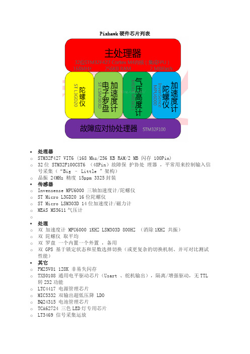
Pixhawk硬件芯片列表•处理器o STM32F427 VIT6 (168 Mhz/256 KB RAM/2 MB 闪存 100Pin)o32位 STM32F100C8T6 (48Pin)故障保护协处理器,平常用来控制输入信号采集(“Big –Little ”架构)o晶振 24MHz 精度 15ppm 3325封装•传感器o Invensense MPU6000 三轴加速度计/陀螺仪o ST Micro L3GD20 16位陀螺仪o ST Micro LSM303D 14位加速度计/磁力计o MEAS MS5611气压计o•处理o双加速度计 MPU6000 1KHZ LSM303D 800HZ (消除1KHZ 共振)o双陀螺仪取平均o双罗盘一个内置一个外置,备用o双 GPS 基于锁定状态和星数选择切换(或更复杂的切换机制、并可对比测试性能)•其它o FM25V01 128K 非易失闪存o TXS0108 通用电平驱动芯片(Usart 、舵机输出),隔离/增强驱动,无TTL 转232功能o LTC4417 电源管理芯片o MIC5332 双输出超低压降 LDOo BQ24315 电池管理芯片o TCA62724 三色LED灯专用芯片o LT3469 信号采集运放o可外接 MS4522D 数字差压空速计(6.6V ADC 输入)3.Pixhawk传感器列表空速计---IIC接口电源管理SMbus---IIC航灯接口---IICBMA180角速度传感器----SPI地磁HMC5883---IIC/SPIL3GD20陀螺仪----SPILSM303D角速度/地磁-----SPI超声波MB12xx----IICMD25---IICMPU6000----SPIMS5611气压计----SPI板载灯控制器TCA62724FMG-----IICPC8574(IIC转并) ----IICPCA9685(IIC/PWM)-----IIC光流模块----IIC4.pixhawk硬件构架5.pixhawk硬件连接关系(1)对照原理图查看所有传感器及接口方式,在F4上的接口;(2)研究下F4和F1的沟通连接方式,以及F1的主要任务;(3)基于以上两点,结合框架文档丰富对硬件架构的认识;规定以下没有括号()的表示网络标号,有括号()的表示具体引脚stm32f427Invensense MPU6000三轴加速度计/陀螺仪PC2(stm32f427)---MPU_CS---CS(MPU6000)PA6(stm32f427)---SPI_INT_MISO---AD0/SDO(MPU6000)PD15(stm32f427)---MPU_DRDY---INT(MPU6000)PA7(stm32f427)---SPI_INT_MOSI---SDA/SDI(MPU6000)PA5(stm32f427)---SPI_INT_SCK---SCL/SCLK(MPU6000)电源VDD_3V3_SENSORSST Micro L3GD20 16位陀螺仪PC13(stm32f427)---GYRO_CS---CS(L3GD20)PA6(stm32f427)---SPI_INT_MISO---SDO/SA0(L3GD20)PB0(stm32f427)---GYRO_DRDY---INT(L3GD20)PA7(stm32f427)---SPI_INT_MOSI---SDA/SDI/SDO(L3GD20) PA5(stm32f427)---SPI_INT_SCK---SCL/SPC(L3GD20)电源VDD_3V3_SENSORSST Micro LSM303D 14位加速度计/磁力计PC15(stm32f427)---ACCEL_MAG_CS---CS(LSM303D)PA6(stm32f427)---SPI_INT_MISO---SDO/SA0(LSM303D)PB4(stm32f427)---ACCEL_DRDY---INT1(LSM303D)PA7(stm32f427)---SPI_INT_MOSI---SDA/SDI/SDO(LSM303D) PA5(stm32f427)---SPI_INT_SCK---SCL/SPC(LSM303D)PB1(stm32f427)---MAG_DRDY---INT2(LSM303D)电源VDD_3V3_SENSORSMEAS MS5611气压计PD7(stm32f427)---BARO_CS---CS(MS5611)PA6(stm32f427)---SPI_INT_MISO---SDO (MS5611)PA7(stm32f427)---SPI_INT_MOSI---SDI/SDA (MS5611)PA5(stm32f427)---SPI_INT_SCK---SCLK(MS5611)电源VDD_3V3_SENSORS存储器PB13(stm32f427)---FRAM_SCK---C(FM25V01)PB14(stm32f427)---FRAM_MISO---Q(FM25V01)PB13(stm32f427)---FRAM_MOSI---D(FM25V01)PD10(stm32f427)---FRAM_CS---S(FM25V01)电源FMU-VDD_3V3高亮LEDPB8(stm32f427)---FMU-I2C1_SCLPB9(stm32f427)---FMU-I2C1_SDAPB10(stm32f427)---FMU-I2C2_SCLPB11(stm32f427)---FMU-I2C1_SDAUSBPA9(stm32f427)---VBUS 电源PA11(stm32f427)---OTG_FS_DMPA12(stm32f427)---OTG_FS_DPPC0(stm32f427)--- VBUS_VALID USB电源有效标志TF卡PC8(stm32f427)---SDIO_D0PC9(stm32f427)---SDIO_D1PC10(stm32f427)---SDIO_D2PC11(stm32f427)---SDIO_D3PC12(stm32f427)---SDIO_CKTEL2_OSDPD8(stm32f427)---FMU-USART3_TXPD9(stm32f427)---FMU-USART3_RXPD11(stm32f427)---FMU-USART3_CTSPD12(stm32f427)---FMU-USART3_RTSTEL1_数传PD3(stm32f427)---FMU-USART3_ CTSPD4(stm32f427)---FMU-USART3_ RTSPD5(stm32f427)---FMU-USART3_TXPD6(stm32f427)---FMU-USART3_RX面板GPSPA0(stm32f427)---FMU-UART4_TXPA1(stm32f427)---FMU-UART4_RX面板CANPD0 (stm32f427)---CAN1_RXPD1 (stm32f427)---CAN1_TX6路辅助PWMPE14(stm32f427)---FMU-CH1PE13(stm32f427)---FMU-CH2PE11(stm32f427)---FMU-CH3PE9 (stm32f427)---FMU-CH4PD13(stm32f427)---FMU-CH5PD14(stm32f427)---FMU-CH6LEDPE12(stm32f427)---FMU-LED_AMBERstm32f427与stm32f100连接PC6(stm32f427)---SERIAL_FMU_TO_IO---PA3(stm32f100) PC7(stm32f427)---SERIAL_IO_TO_FMU---PA2(stm32f100) stm32f1008路主PWMPA0(stm32f100)---IO-CH1PA1(stm32f100)---IO-CH2PB8(stm32f100)---IO-CH3PB9(stm32f100)---IO-CH4PA6(stm32f100)---IO-CH5PA7(stm32f100)---IO-CH6PB0(stm32f100)---IO-CH7PB1(stm32f100)---IO-CH8安全开关PB5(stm32f100)---SAFTYLEDPB13(stm32f100)---IO-LED_SAFTY PB14(stm32f100)---IO-LED_BLUE PB15(stm32f100)---IO-LED_AMBER PPM接收PA8(stm32f100)---PPM_INPUTS.BUSPB4(stm32f100)---SBUS_OUTPUT_EN PB10(stm32f100)---SBUS_OUTPUT PB11(stm32f100)---SBUS_INPUT JTAG电源IO-VDD_3V3PA13(stm32f100)---IO-SWDIOPA14(stm32f100)---IO-SWCLKPB3(stm32f100)---IO-SWO卫星接收机PA10(stm32f100)---IO-USART1_RX PB15(stm32f100)---IO-LED_AMBERPA10(stm32f100)--- VDD_3V3_SPEKTRUM 电源。
FLASH和主控关系

描述:图1,TSOP48封装的FLASH 图片:描述:图2,8位和16位FLASH对比图片:描述:图3,FLASH引脚说明图片:一,基础知识现在数码设备上常用的FLASH基本都是TSOP48封装,其引脚比较密,焊接的时候最好用尖头的烙铁。
见图1,闪存芯片,不同容量是Pin to Pin 的,即芯片的封装、引脚的功能、外围电路都是基本相同的。
可以说是硬件间的兼容,这为FLASH代换提供了基础。
常用的FLASH都属于并行FLASH,是同时可以传输多位数据,分为8位和16位,8位就是说FLASH 有8个数据脚(I/O0-I/O7)也有的是标为(D0-D7),一次可以同时传输8位数据。
16位以此类推。
常用设备中用8位的较多,占到9成以上。
在图2中可以看到,除了数据脚,8位和16位的FLASH其他引脚是一致的。
在图2中我们发现,FLASH的48个引脚中很多都是空的(NC),特别是8位的FLASH(因为16位FLASH用得很少,所以下面的说明都是以位的FLASH作为例子),一共才用了19个脚,这其中我们需要了解的只有2个,CE和R/B脚。
这2个脚对FLASH代换升级有较大影响。
CE是片选,和主控的CE脚相连,只有CE被主控相连选中,FLASH才能工作。
R/B:就绪/忙输出,R/B的输出能够显示设备的操作状态。
R/B处于低电平时,表示有编程、擦除或随机读操作正在进行。
操作完成后,R/B会自动返回高电平。
由于该端是漏极开路输出,所以即使当芯片没有被选中或输出被禁止时,它也不会处于高阻态。
描述:图4,4CE的FLASH 图片:描述:图5,2CE的FLASH 图片:描述:图6,1CE的FLASH图片:前面提到,闪存芯片,不同容量是Pin to Pin 的,即芯片的封装、引脚的功能、外围电路都是基本相同的。
为什么说是基本相同呢?因为不同容量FLASH可能采用的管芯数量不同,从而造成引脚的细微差别。
什么是管芯呢?这要从闪存起源说起。
3-bit-per-cell NAND闪存
特 征 , 试 验证 实 , 以 有 效 地进 行字 符 识 别 。 且 当纸 币 序 经 可 并 列 号 图像 出 现较 大 噪 声 甚 至 字 体 出 现 不 规 则 情 况 时 , 字 符 该 提 取 方 法 具 有 很 高 的 抗 干 扰 能 力 。同 时 , 于径 向 基 函 数 神 由
N N 闪存 , N N 设 备拥 有 业界 最 大的 容 量 和 最 小 的 尺 寸 。两 家公 司 已将 初 始 产 品 样 品 送 到 部 分 客 户 手 中 。美 光 与 英特 A D 该 A D
尔预 计 在 今 年 年 底 时量 产该 产品 。
与 竞 争 对 手 U B、D Scr ii1闪存 卡和 消 费 电子 产 品 相 比 , 推 出的 2 m 6 b3b c存 储 设 备 的 性 价 比更 高且 S S (eueDgt ) a 新 5n 4G p 存 储 量 更 大 。 闪存 主要 用 于存 储 数 据 、 片或 其 它 多媒 体 , 计 算 机 应 用 和数 码 设 备 ( 码 相 机 、 携 式媒 体播 放 器 、 携 式 数 照 如 数 便 便
(4 :5 — 5 . 2 ) 1 3 1 5
YUAN e— i W iq .A a tr c g to y tm o a rc r nc fs e o niin s se fr p pe ure y
【3 i o 1】Bs p C M.N ua n tok rpt r eont nM】 h e r e rsf a e rcg io 【 . l w o tn i
经 网络 结 构 简 单 , 别 率 高 , 不 论 在 P 识 故 C或 者 嵌 入 式 的 应 用
【0 王 瑞 玲 . 币序 列 号 识 别 方 法【1哈 尔滨 : 尔滨 工 业 大 11 纸 D. 哈
Apricorn 硬盘加密 USB 闪存驱动器说明说明书

ON-THE-FLY 256-BIT AES-XTS HARDWARE ENCRYPTION SOFTWARE-FREE INSTALLATION & OPERATION; COMPLETELY CROSS-PLATFORM COMPATIBLE HIGH-QUALITY RUGGED ALUMINUM HOUSING Water and Dust Resistant EMBEDDED 7-16 DIGIT PIN AUTHENTICATION No Security Parameters Shared with HostsADMIN MODE FOR SECURE DEPLOYMENTINDEPENDENT USER AND ADMIN PINSFORCED ENROLLMENT AT FIRST USETOUGH EPOXY INTERNAL FILLING FOR PHYSICAL-ATTACK PROTECTIONBRUTE-FORCE PROTECTIONSELF-DESTRUCT PIN FEATURE COMPATIBLE WITH ANY OS Windows ®, Mac ®, Linux SUPER-FAST USB 3.0 10X Faster than USB 2.0VARIABLE TIMING CIRCUIT LOCK-OVERRIDE MODE DRIVE-RESET FEATURE AUTO-LOCK FEATURE READ-ONLY MODE Visit our web site at or call 1-800-458-5448©2014 Apricorn, Inc. Corporate Offices: 12191 Kirkham Rd., Poway, CA. 92064HARDWARE ENCRYPTED USB FLASH DRIVE Inside This Tiny Key is a World Of Advanced Data Protection.Software-free operation, cross-platform compatibility, USB 3.0 speed, increased capacities of up to 240GB, plus a host of high-level security features that you’d never expect to find in a itary Grade 256-bit AES XTS Hardware Encryption: All data on theAegis Secure Key is encrypted on-the-fly with built-in 256-bit AES XTS.Software-Free Design: The Aegis Secure Key is ready to use right out of the box–no software, no drivers, no updates involved. It can even be utilized where no keyboard is present (e.g., cockpits, medical equipment, A V gear.) Completely cross-platform compatible, the Aegis Secure Key excels just about anywhere–PCs, MACs, Linux, or any OS with a powered USB port and a storage file system. Embedded Keypad: All PIN entries and controls are performed on the keypad of the Aegis Secure Key. Since there is no host involvement in the key’s authentication or operation, the risk of software hacking and key-logging is completely circumvented.Super Tough, Inside and Out: IP-58 certified as tough enough to go anywhere, the Aegis Secure Key’s resilient design makes it perfect for travel. Its rugged, extruded aluminum casing is resistant to dust and water, and the keypad is wear-resistant. Inside, another layer of protection is added with the injection of a tough epoxy compound to prevent physical access to the key’s encryption circuitry. Independent User and Admin PINs: The Aegis Secure Key can be configured independent User and Admin PINs, making it an ideal device for corporate and government deployment. Should the User forget his or her PIN, the drive can still be unlocked with the Admin PIN and a new User PIN can be created.Auto-Lock Feature: Locks automatically whenever it’s unplugged from its powered USB port, and is further programmable to lock after a predetermined period of inactivity.Drive Reset Feature: Effectively clears both the User and Admin PINs, performs a crypto-erase onthe drive, creates a new randomly generated encryption key, and allows the drive to be redeployed. Capable of generating an infinite number of randomly generated encryption keys, The Aegis Secure Key permits the admin to reset the drive as many times as desired.Brute-Force Protection: After a predetermined number (programmable; up to 20) of incorrect PIN entry attempts, the Aegis Secure Key will conclude that it is under Brute Force Attack and will respond by performing a crypto-erase – deleting the encryption key which will render all of the key’s data useless. VTC Technology: Apricorn’s Variable Time Circuit (VTC) technology is designed to thwart Timing Attacks aimed at accessing the drive by studying usage patterns and infiltrating the Secure Key’s electronics. Lock-Override Mode Feature: Designated for specific cases in which the key needs unlocked, e.g., during reboot, passing the key through a virtual machine, or other similar situations that would normally prompt the key to automatically lock. When enabled, Lock-Override Mode allows the key to remain unlocked through USB port re-enumeration and will not re-lock until USB power is interrupted.Read-Only Mode Feature: Perfect for accessing data on the key in a public setting to protect against USB viruses or Trojan attachments. Particularly important in forensics, Read-Only Mode is ideal for applications that require data to be preserved in its original, unaltered state and can’t be overwritten or modified.Self-Destruct Feature: The last line of defense for data security where all of the drive’s contents must be wiped to avert breach. The Secure Key’s Self-Destruct PIN defends against physically compromising situations by erasing the key’s contents, leaving it in normal working order and to appear as if it has yet to be deployed.Aegis Secure Key 3.0WORKS WITH:For more information on Aegis Secure Key and other innovativeApricorn products visit our web site at or call 1-800-458-5448©2014 Apricorn, Inc. Corporate Offices: 12191 Kirkham Rd., Poway, CA. 92064*One gigabyte (GB) = one billion bytes; accessible capacity will be less and actual capacity depends on the operating environment and formatting.STEP 1Enter your PINPlug & Play Press Lock or Unplug to Lock STEP 2STEP 3rev 09-18-15。
固态硬盘闪存大揭秘:白片、黑片、划线片、拆机片

固态硬盘闪存大揭秘:白片、黑片、划线片、拆机片我们在选择SSD的时候,最为关注的除了SSD主控,便是SSD 的闪存了。
SSD的闪存类型和闪存芯片级别是SSD性能的根本。
SSD的闪存类型,市场上主流的无非四种:TLC、3D TLC、MLC、3D MLC(按照闪存性能从低到高排列)。
准确的说是三种,据我所知采用3D MLC NAND的,目前市面上好像只有阿斯加特AN Series M.2 SSD 256G这一款。
据说是因为全球首发,打开销量才这样不惜血本。
SSD闪存类型没什么好说。
我们今天要讲的是,SSD闪存的芯片级别。
闪存的芯片级别分为:正片:正片闪存通过了全部产品测试,然后激光打标了产品信息。
白片:白片是在测试时部分测试未通过的闪存芯片。
这些闪存芯片再经过一些测试后,如果不影响使用,就打标并和正片一样流向市场。
由于全球晶圆紧缺,闪存价格飞涨,正片供不应求。
正片做SSD 成本高昂,而且还没货。
因此市面上主流的SSD基本上都是使用的白片闪存。
白片闪存相对正片在价格上有优势,做成SSD同样有价格优势。
在性能上,好的白片性能与正片相差无几。
白片SSD可以说是物美价廉。
既然市面上白片很普遍。
那怎样去识别白片呢?我们拿镁光的白片来说。
镁光白片,网友称之为大S或者小S。
不是徐熙媛,也不是徐熙娣,是SpecTek。
SpecTek是镁光旗下的一个子公司。
镁光的白片就是交给它来进行各种测试,在测试完毕后上市的。
测试完以后SpecT ek会给白片闪存一个物料编号。
下面是SpecTek的物料编码规则。
对于这个编码规则,大家不用了解太多。
我们稍微讲一些重点问题。
镁光的SpecTek闪存芯片,物料编码前两位只能是FN/FT/FB/FX,如果不是,可能你就遇到黑片了。
由于上面说到,镁光的白片几乎都经过SpecTek才出货的,所以我们通过识别闪存物料号的前两位,也基本上能够识别出镁光的白片和黑片了。
镁光的SpecTek闪存芯片第4位是显示闪存的类型。
- 1、下载文档前请自行甄别文档内容的完整性,平台不提供额外的编辑、内容补充、找答案等附加服务。
- 2、"仅部分预览"的文档,不可在线预览部分如存在完整性等问题,可反馈申请退款(可完整预览的文档不适用该条件!)。
- 3、如文档侵犯您的权益,请联系客服反馈,我们会尽快为您处理(人工客服工作时间:9:00-18:30)。
Secure Digital I/O Card DescriptionSecure Digital Input/Output [SDIO] is a flash based removable memory card. The card format may also be used for other device functions in addition to data storage. Secure Digital IO uses a 9-Pin connector [1 row of 9 pins]. SDIO is based on the Secure Digital SD card. SDIO is compatible with the SD memory card, and fits in the same socket.The Secure Digital I/O card dimensions are: 24mm wide x 32mm long x 2.1mm thick.There are two types of SDIO cards; a full-speed version, and a slow-speed version. The full-speed version will operate with a 1-bit and 4-bit SD transfer mode, both with a clock ranging from 0Hz to 25MHz. The 4-bit version operating at 25MHz has a transfer rate of 100Mbps. The slow-speed version will use the 1-bit mode and may have the 4-bit mode, but only operates at a transfer rate of between 0Hz and 400kHz. The slow-speed version is not intended for memory functions. The SDIO card support the SPI bus interface. The SDIO mechanical form factor is shown above; however a few gaps "lock notches" are not shown. The SDIO card may exceed 24mm in width after 37mm in length, and the width may be thicker then 2.1mm after 37mm in lengthT he Secure Digital memory card is a memory specifically developed to meet security requirements which have appeared in the field of electronic audio and video devices. It includes a Copyright protection mechanism which complies with the SDMI standard (Secure Digital Music Initiative). The file protection and encryption system (CPRM: Content Protection for Recordable Media) is integrated into the SD card. The SD card's interface supports standard MMC card operations.Secure Digital I/O Card, Pin OutMemory Stick description and Pin OutMemory Stick is another type of Removable NAND-type small flash memory card format which was introduced in 1998. There are a few different Memory Stick formats: the Standard-size Memory Stick media measures 50.0mm x 21.5mm x 2.8mm [Width x Height x Depth], and the Memory Stick Duo media measures 31.0mm x 20.0mm x 1.6mm [Width x Height x Depth]. Pins 1 and 10 are longer then the other pins so ground is the first pin to make contact and the last to break contact. Pin 6 is recessed and make contact last as the stick is inserted. The pins are flat electrodes. The maximum transfer rate is 2.54MBps, with a maximum clock frequency of 40MHz. Memory Stick requires a power supply voltage of 2.7v to 3.6 volts.Memory Stick - Memory Stick Pro - 10 pin connectorNote: both Pin 1 and Pin 10 shall be connected to VSS.Memory Stick, Memory Stick Duo, MagicGate, MagicGate Memory Stick, MemoryStick PRO are registered trademarks or trademarks of Sony Corporation.Multi Media Card, Pin OutMultiMedia Card uses a 7-Pin connector [1 rows of 7 pins]. The 7-pin connector is on 2.5-mil centers. The seven pin interface consists of three pins dedicated to the SPI serial bus [SCK, SI, and SO], a Chip Select signal [CS], a Chip Reset [RESET], a Write Protect line [WP], and an output Ready/Busy [RDY/Busy] signal. All of the control signals execpt the RDY signal are active low. The SPI interface uses the Serial Clock [SCK] line, Serial Input [SI], and the Serial Output [SO] line. How ever the physical DataFlash card does not have all the signals listed above, refer to the pinout table shown below. A few of the signals listed above may only be found on the DataFlash Integrated Circuits [ICs]. A smaller form factor of MMC is called Reduced Size MultiMedia Card [RS-MMC]. The RS-MMC card is 24mm x 16mm x 1.5mm. The RSMMC remains pin compatible with the MMC module, but shorterThe newer versions of the standard; MMCplus, MMCmobile and MMCmicro, offer the higher transfer speeds up to 52MB/sec, or 416 Mbits/sec, and support for dual-voltage operation (1.8 and 3/3.3V), and multiple bus widths (x1, x4 and x8 bit). MMCplus, MMCmobile and MMCmicro utlize 13 pins while remaining backwards compatible with the previous version of 7-pin MMC cardsMultiMedia Card - 7 pin connectorSmartMedia Description and Pin OutSmartMedia is another type of Removable NAND-type small flash memory card format. The SmartMedia device size is 45 mm x 37 mm x 0.76 mm [thick]. SmartMedia cards operate using either 3.3 volt or 5 volt. Solid State Floppy Disk Card [SSFDC] is the old name for SmartMedia, which was changed in 1996. SSFDC was Developed by Toshiba Corp. Current SmartMedia storage format include 16-Mbit, 32-Mbit, and 64-Mbit NAND-type flash memory chips. The SmartMedia card does not use a connector, instead it uses a contact area as shown in the graphic below. The graphic also defines the pinout.Pin assignment of 5V and 3.3V SmartMedia TM。