SiC功率器件产品选型手册
碳化硅功率器件 最大频率
碳化硅(SiC)功率器件因其高电子迁移率、高击穿电压、高热稳定性和低损耗等特性而在高频、高功率应用中表现出优异的性能。
这些特性使得SiC器件能够在高频率下工作,从而提高电力转换效率,降低系统尺寸和重量,减少能源消耗。
碳化硅功率器件的最大工作频率取决于多个因素,包括器件的设计、制造工艺、材料质量、电路设计和应用条件等。
一般来说,SiC器件可以工作的频率范围远高于传统的硅(Si)功率器件。
对于特定的SiC器件,其最大工作频率可能在几百kHz到几MHz之间,甚至更高。
例如,对于SiC肖特基二极管(SiC Schottky Diode),其开关速度可以达到几百kHz甚至更高,这使得它们非常适合用于高频开关应用,如可再生能源、电动汽车、高频通信和工业自动化等。
而对于SiC金属氧化物半导体场效应晶体管(SiC MOSFET),其开关速度通常较低,可能在几十kHz到几MHz之间,但它们仍然比传统的Si MOSFET具有更高的开关频率能力。
实际应用中,除了器件本身的物理特性,电路设计、驱动电路、散热条件等因素也会限制器件的实际工作频率。
因此,确定SiC功率器件的最大工作频率时,需要考虑这些综合因素。
sic437规格书
sic437规格书SIC437规格书是指由美国半导体工业协会(SIA)和欧洲电子元器件工业协会(EECA)共同制定的半导体产品的标准规范。
该规格书的制定旨在规范半导体产品的设计、生产、测试和质量控制等方面的标准,以确保半导体产品的性能和质量达到了一定的水平,同时也方便半导体相关行业企业的生产和管理。
具体而言,SIC437规格书包括了以下内容:1.产品类型:此规范适用于单晶硅、多晶硅、氮化硅等材料生产的半导体知识产权产品,例如集成电路、光电器件、功率半导体等。
2.产品特性:该规范对半导体产品的电气和物理特性进行了严格的规定,例如工作电压、电流、功率、温度范围、封装方式、尺寸等。
3.测试规范:该规范对半导体产品的测试方法和测试环节进行了规定,包括测试设备、测试方式、测试流程、测试结果分析等。
4.质量标准:该规范对半导体产品的生产过程和质量进行了详细的规范,包括原材料的选择、生产工艺的规范、质量控制流程等,以确保产品的质量稳定和可靠。
5.其他:该规范还包括了一些其他的工业标准,例如耐受性规范、环境适应性规范、封装标准等,以保证半导体产品的可靠性和性能稳定性。
SIC437规格书对于半导体相关企业和行业来说非常重要,它不仅规范了产品的设计和生产过程,提高了产品的质量和稳定性,也为行业间的交流和合作提供了一个标准的基础。
同时,在国际贸易中,也可以作为一项交流和合作的重要工具,为企业之间的商业合作提供更为通畅的环境。
总之,SIC437规格书的制定凝聚了国际半导体行业的智慧和努力,它的出现标志着半导体行业产品标准化的进一步发展和提高,对于半导体企业和相关行业的可持续发展有着积极的推动作用。
碳化硅sbd规格书导读
碳化硅sbd规格书导读一、引言随着科技的飞速发展,碳化硅(SiC)半导体材料因其卓越的性能逐渐成为业界关注的焦点。
其中,碳化硅肖特基二极管(SBD)在电子行业中的应用越来越广泛。
本文将为大家详细解读碳化硅SBD规格书,帮助大家更好地了解这一材料及其应用。
二、碳化硅SBD简介1.碳化硅材料特点碳化硅(SiC)具有良好的导电性能、高热导率、高击穿电压、低导通电阻等特点。
这些特性使得碳化硅器件在高温、高功率、高压等应用场景下具有优越的性能。
2.SBD结构和工作原理碳化硅SBD的结构类似于普通肖特基二极管,由n型碳化硅基片、p型碳化硅层和n+型碳化硅接触层组成。
其工作原理是利用p型层与n型层之间的PN结,实现电子与空穴的复合,从而实现电流的流动。
三、碳化硅SBD规格书主要内容1.参数分类碳化硅SBD规格书主要包括以下参数:- 正向电压(V Forward)- 反向电压(V Reverse)- 漏极电流(ID)- 开关速度(ts)- 热阻(Rth)- 寿命(Tb)2.参数解读通过对这些参数的解读,可以了解到碳化硅SBD的电气特性、热性能等方面的信息,为器件选型和应用提供依据。
3.应用场景和建议碳化硅SBD规格书还会给出推荐的应用场景和注意事项,帮助用户正确选用合适的碳化硅SBD。
四、碳化硅SBD在电子行业的应用1.电源管理碳化硅SBD在电源管理领域具有很高的潜力,可以应用于开关电源、直流-直流转换器、充电器等场景,提高能源转换效率。
2.电动汽车碳化硅SBD在电动汽车中的应用主要包括电池保护、电机控制、充电系统等,有助于减小系统体积、降低能耗。
3.工业控制碳化硅SBD在工业控制领域可应用于变频器、逆变器等高压、高功率场景,提高系统性能。
五、碳化硅SBD的未来发展趋势随着碳化硅材料制备技术的不断进步,碳化硅SBD的成本将逐步降低,性能将进一步提高。
在未来,碳化硅SBD在电子、能源、交通等领域具有广阔的应用前景。
MSCSM120TAM11CTPAG 三相三导线SiC MOSFET电源模块说明书

MSCSM120TAM11CTPAGDatasheet Triple Phase Leg SiC MOSFET Power ModuleJanuary2020ContentsRevision History (1)1.1Revision 1.0 (1)Product Overview (2)2.1Features..............................................................................................................................................................32.2Benefits...............................................................................................................................................................32.3Applications.. (3)Electrical Specification (4)3.1SiC MOSFET Characteristics (Per MOSFET).........................................................................................................43.2Reverse SiC Diode Ratings and Characteristics (Per SiC Diode)..........................................................................63.3Thermal and Package Characteristics.................................................................................................................63.4Typical SiC MOSFET Performance Curves...........................................................................................................83.5Typical SiC Diode Performance Curves. (11)Package Specifications (12)4.1Package Outline Drawing (12)Contents1Revision HistoryThe revision history describes the changes that were implemented in the document.The changes are listed by revision,starting with the most current publication.1.1Revision 1.0Revision 1.0was published in January 2020.It is the first publication of this document.Revision HistoryThe MSCSM120TAM11CTPAG device is a3phase leg1200V/251A full Silicon Carbide(SiC)power module.Figure1•MSCSM120TAM11CTPAG Electrical SchematicFigure2•MSCSM120TAM11CTPAG Pinout LocationAll ratings at T J=25°C,unless otherwise specified.Caution:These devices are sensitive to electrostatic discharge.Proper handling procedures should befollowed.2.1FeaturesThe following are key features of the MSCSM120TAM11CTPAG device:•SiC Power MOSFET◦Low R DS(on)◦High temperature performance•SiC Schottky Diode◦Zero reverse recovery◦Zero forward recovery◦Temperature Independent switching behavior◦Positive temperature coefficient on VF•Very low stray inductance•Internal thermistor for temperature monitoring•Aluminum nitride(AlN)substrate for improved thermal performance 2.2BenefitsThe following are benefits of the MSCSM120TAM11CTPAG device:•High power and efficient converters and inverters•Outstanding performance at high frequency operation•Direct mounting to heatsink(isolated package)•Low junction-to-case thermal resistance•Solderable terminals for power and signal,for easy PCB mounting•Low profile•RoHS compliant2.3ApplicationsThe MSCSM120TAM11CTPAG device is designed for the following applications:•Uninterruptible power supplies•Switched Mode power supplies•EV motor and traction drive•Welding converters3Electrical SpecificationsThis section shows the electrical specifications of the MSCSM120TAM11CTPAG device.3.1SiC MOSFET Characteristics (Per MOSFET)The following table shows the absolute maximum ratings per MOSFET of the MSCSM120TAM11CTPAG device.Table 1•Absolute Maximum RatingsUnit Max Ratings ParameterSymbol V 1200Drain-source voltage V DSS A2511T C =25°C Continuous drain currentI D2001T C =80°C500Pulsed drain current I DM V –10/25Gate-source voltage V GS mΩ10.4Drain-source ON resistance R DSon W 1042T C =25°CPower dissipationP DNote:1.Specification of SiC MOSFET device,but output current must be limited due to size of power connectors.The following table shows the electrical characteristics per MOSFET of the MSCSM120TAM11CTPAG device.Table 2•Electrical CharacteristicsUnit Max Typ MinTest Conditions CharacteristicSymbol µA 30030V GS =0V;V DS =1200V Zero gate voltage drain current I DSS mΩ10.48.4T J =25°C V GS =20V I D =120ADrain-source on resistanceR DS(on)13.4T J =175°CV 2.81.8V GS =V DS ,I D =3mA Gate threshold voltage V GS(th)nA300V GS =20V,V DS =0VGate-source leakage currentI GSSThe following table shows the dynamic characteristics per MOSFET of the MSCSM120TAM11CTPAG device.Table 3•Dynamic CharacteristicsUnit MaxTyp MinTest Conditions Characteristic Symbol pF9060V GS =0V V DS =1000V Input capacitance C iss 810Output capacitance C oss f =1MHz75Reverse transfer capacitance C rss nC696V GS =–5V/20V V Bus =800V Total gate charge Q g 123Gate-source charge Q gs I D =120A 150Gate-drain charge Q gd ns 30V GS =–5V/20V V Bus =600V Turn-on delay time T d(on)30Rise time T r I D =150A50Turn-off delay time T d(off)R Gon =2.7Ω;R Goff =1.6Ω25Fall time T f mJ 3.0T J =150°C Inductive switching V GS =–5V/20V Turn on energy E on mJ 2.0T J =150°CTurn off energyE offV Bus =600V I D =150A R Gon =2.7ΩR Goff =1.6ΩΩ2.0Internal gate resistanceR Gint °C/W0.144Junction-to-case thermal resistanceR thJCThe following table shows the body diode ratings and characteristics per MOSFET of the MSCSM120TAM11CTPAG device.Table 4•Body Diode Ratings and CharacteristicsUnit MaxTyp MinTest Conditions Characteristic Symbol V4.0V GS =0V;I SD =120A Diode forward voltageV SD4.2V GS =–5V ;I SD =120Ans 90I SD =120A;V GS =–5V V R =800V;d iF /dt =3000A/μsReverse recovery time t rr nC 1650Reverse recovery charge Q rr A40.5Reverse recovery currentI rr3.2Reverse SiC Diode Ratings and Characteristics(Per SiC Diode)The following table shows the SiC diode ratings and characteristics per SiC diode of theMSCSM120TAM11CTPAG device.Table5•Reverse SiC Diode Ratings and Characteristics(per SiC diode)CharacteristicSymbolTest ConditionsTypMaxMinUnit V RRMV Peak repetitive reverse voltage1200Reverse leakage currentI RMV R=1200VT J=25°CμA40015250T J=175°CAI FDC forward current50T C=100°CI F=50AV FDiode forward voltageV1.81.5T J=25°C2.1T J=175°CQcTotal capacitive chargenCV R=600V224Total capacitanceCpF246f=1MHz,V R=400V182f=1MHz,V R=800VR thJC0.573Junction-to-case thermal resistance°C/W 3.3Thermal and Package CharacteristicsThe following table shows the package characteristics of the MSCSM120TAM11CTPAG device.Table6•Package CharacteristicsMaxUnit SymbolCharacteristicMinV ISOLV RMS isolation voltage,any terminal to case t=1min,50Hz/60Hz4000Operating junction temperature rangeT J–40°C175Recommended junction temperature under switching conditionsT JOP–40T Jmax–25 T STGStorage temperature range–40125 T COperating case temperature–40125To heatsinkTorqueMounting torqueN.mM653Wtg250Package weightThe following table shows the temperature sensor NTC(see application note APT0406on)of the MSCSM120TAM11CTPAG device.Table7•Temperature Sensor NTCSymbolCharacteristicTypMaxMinUnit Resistance at25°CR2550kΩ∆R25/R255% B25/85T25=298.15K3952K∆B/BT C=100°C4%3.4Typical SiC MOSFET Performance CurvesThis section shows the typical SiC MOSFET performance curves of the MSCSM120TAM11CTPAG device.Figure3•Maximum Thermal ImpedanceFigure4•Output Characteristics,T J=25°CFigure6•Normalized R DS(on)vs.TemperatureFigure8•Switching Energy vs.Rg Figure9•Switching Energy vs.CurrentFigure10•Capacitance vs.Drain Source VoltageFigure12•Body Diode Characteristics,T J=25°C°CFigure16•Operating Frequency vs.Drain Current3.5Typical SiC Diode Performance CurvesThis sections shows the typical SiC diode performance curves of the MSCSM120TAM11CTPAG device.Figure17•Maximum Thermal ImpedanceFigure18•Forward CharacteristicsThis section shows the package specification of the MSCSM120TAM11CTPAG device.4.1Package Outline DrawingThe following figure illustrates the package outline of the MSCSM120TAM11CTPAG device.The dimensionsin the following figure are in millimeters.Figure20•Package Outline Drawingat .Microsemi's product warranty is set forth in Microsemi's Sales Order Terms and rmation contained in this publication is provided for the sole purpose of designing with and using Microsemi rmation regarding device applications and the like is provided only for your convenience and may be superseded by updates.Buyer shall not rely on any data and performance specifications or parameters provided by Microsemi.It is your responsibility to ensure that your application meets with your specifications.THIS INFORMATION IS PROVIDED "AS IS."MICROSEMI MAKES NO REPRESENTATIONS OR WARRANTIES OF ANY KIND WHETHER EXPRESS OR IMPLIED,WRITTEN OR ORAL,STATUTORY OR OTHERWISE,RELATED TO THE INFORMATION,INCLUDING BUT NOT LIMITED TO ITS CONDITION,QUALITY ,PERFORMANCE,NON-INFRINGEMENT,MERCHANTABILITY OR FITNESS FOR A PARTICULAR PURPOSE.IN NO EVENT WILL MICROSEMI BE LIABLE FOR ANY INDIRECT,SPECIAL,PUNITIVE,INCIDENTAL OR CONSEQUENTIAL LOSS,DAMAGE,COST OR EXPENSE WHATSOEVER RELATED TO THIS INFORMATION OR ITS USE,HOWEVER CAUSED,EVEN IF MICROSEMI HAS BEEN ADVISED OF THE POSSIBILITY OR THE DAMAGES ARE FORESEEABLE.TO THE FULLEST EXTENT ALLOWED BY LAW,MICROSEMI’S TOTAL LIABILITY ON ALL CLAIMS IN RELATED TO THIS INFORMATION OR ITS USE WILL NOT EXCEED THE AMOUNT OF FEES,IF ANY ,YOU PAID DIRECTLY TO MICROSEMI FOR THIS e of Microsemi devices in life support,mission-critical equipment or applications,and/or safety applications is entirely at the buyer’s risk,and the buyer agrees to defend and indemnify Microsemi from any and all damages,claims,suits,or expenses resulting from such use.No licenses are conveyed,implicitly or otherwise,under any Microsemi intellectual property rights unless otherwisestated.Microsemi2355W.Chandler Blvd.Chandler,AZ 85224USAWithin the USA:+1(480)792-7200Fax:+1(480)792-7277 ©2020Microsemi andits corporate affiliates.All rights reserved.Microsemi and the Microsemi logo aretrademarks of Microsemi Corporation and itscorporate affiliates.All other trademarks andservice marks are the property of theirrespective owners.Microsemi Corporation,a subsidiary of Microchip Technology Inc.(Nasdaq:MCHP),and its corporate affiliates are leading providers of smart,connected and secure embedded control solutions.Their easy-to-use development tools and comprehensive product portfolio enable customers to create optimal designs which reduce risk while lowering total system cost and time to market.These solutions serve more than 120,000customers across the industrial,automotive,consumer,aerospace and defense,communications and computing markets.Headquartered in Chandler,Arizona,the company offers outstanding technical support along with dependable delivery and quality.Learn more at .MSCC-0344-DS-01064-1.0-0120Legal。
sicmos栅极电阻选型标准
sicmos栅极电阻选型标准摘要:I.前言- 栅极电阻在SiCmos 器件中的重要性II.SiCmos 栅极电阻选型标准1.电阻值选择- 影响电阻值的参数- 电阻值的选择方法2.功率处理能力- 决定因素- 选型建议3.工作温度- 温度对电阻性能的影响- 选型建议4.封装选择- 常见封装类型- 选型建议III.总结- 栅极电阻选型的关键要点- 未来发展趋势正文:I.前言栅极电阻在SiCmos 器件中具有至关重要的作用。
作为功率半导体器件的关键组成部分,栅极电阻对器件的性能和可靠性具有重要影响。
因此,在选择SiCmos 栅极电阻时,必须依据一定的选型标准以保证器件的性能和可靠性。
II.SiCmos 栅极电阻选型标准1.电阻值选择电阻值是SiCmos 栅极电阻选型的关键参数。
电阻值的选择需考虑多种因素,如器件的额定电压、电流,以及控制电路的驱动能力等。
合适的电阻值应保证在正常工作条件下,驱动电流足够大,从而使得器件能可靠地工作。
2.功率处理能力SiCmos 栅极电阻需要承受较高的功率处理能力。
这一参数主要由电阻材料、电阻值和额定电压决定。
在选型时,应确保所选电阻器的功率处理能力不低于器件的最大功率需求,以防止因过载导致的损坏。
3.工作温度工作温度对SiCmos 栅极电阻的性能具有重要影响。
高温环境可能导致电阻性能降低,影响器件的工作可靠性。
因此,在选型时,应充分考虑电阻器的工作温度范围,确保其在器件的工作温度范围内能稳定工作。
4.封装选择合适的封装形式对于SiCmos 栅极电阻的性能和可靠性同样重要。
常见的封装类型有贴片式、插件式等。
在选型时,应根据实际应用需求和安装条件选择合适的封装形式。
III.总结SiCmos 栅极电阻的选型是器件设计和应用过程中的关键环节。
合理的选型能够保证器件的性能和可靠性,提高整个系统的稳定性和安全性。
在选型过程中,需综合考虑电阻值、功率处理能力、工作温度和封装形式等因素,确保所选电阻器满足实际应用需求。
sic功率器件应用场景

标题:应用场景:SIC功率器件SIC(碳化硅)功率器件是一种新型的半导体功率器件,具有许多优点,如高温稳定性、高频操作能力和低开关损耗等。
由于这些独特的特性,SIC功率器件在许多领域都有广泛的应用。
以下是一些常见的SIC功率器件应用场景:1.工业领域: SIC功率器件在工业领域中的应用非常广泛。
例如,它们可以用于驱动电机和控制电流的变频器。
由于SIC器件具有高温稳定性和高频操作能力,它们在高温和高频环境下可以提供更高的效率和更好的性能。
此外,SIC器件还可以用于工业照明系统和电力传输设备等高功率应用。
2.电动车和混合动力车:由于SIC功率器件具有低开关损耗和高温稳定性,它们在电动车和混合动力车中的应用越来越受到重视。
SIC器件可以提高电动车系统的效率并延长电池寿命。
此外,SIC器件还可以减小电动车的体积和重量,提高整体性能。
3.新能源发电:在新能源发电领域,如风能和太阳能发电中,SIC功率器件也有广泛的应用。
SIC器件可以提高能量转换效率,减少能量损失。
此外,由于SIC器件的高温稳定性,它们可以在高温环境下运行,适应太阳能发电板和风力发电机等设备的工作条件。
4.航空航天和国防领域:在航空航天和国防领域,对高温和高频操作能力的需求非常高。
SIC功率器件可以满足这些需求,并提供更高的性能和可靠性。
它们可以用于飞机和导弹的电力系统,提供更高的功率密度和更好的热管理。
5.医疗设备: SIC功率器件还可以在医疗设备中得到应用。
例如,它们可以用于高频电切和电凝手术仪器,提供更高的精确性和效率。
此外,SIC器件还可以用于医疗成像设备和激光治疗系统等高功率应用。
总结: SIC功率器件在工业、电动车、新能源发电、航空航天和国防、医疗设备等领域都有广泛的应用。
它们的高温稳定性、高频操作能力和低开关损耗等特点使其成为许多应用场景的理想选择。
随着技术的不断发展,SIC功率器件的应用前景将继续扩大。
sic mosfet 器件手册解读
一、SIC MOSFET器件简介1. 介绍SIC MOSFET器件的基本结构和工作原理2. 分析SIC MOSFET器件的优势和应用领域二、SIC MOSFET器件的性能参数解读1. 主要包括导通特性、开关特性、静态特性和动态特性等方面的参数2. 对每个性能参数进行详细解读和分析三、SIC MOSFET器件的设计与制造工艺1. 介绍SIC MOSFET器件的设计流程和关键技术2. 分析SIC MOSFET器件的制造工艺及其对器件性能的影响四、SIC MOSFET器件在电力电子领域的应用1. 分析SIC MOSFET器件在变流器、逆变器、充电桩等领域的应用2. 探讨SIC MOSFET器件在电力电子领域的发展趋势五、SIC MOSFET器件的可靠性与封装技术1. 分析SIC MOSFET器件的可靠性测试技术和参数2. 探讨SIC MOSFET器件的封装技术及其对器件可靠性的影响六、SIC MOSFET器件的市场前景与发展趋势1. 分析SIC MOSFET器件在全球范围内的市场占有率和竞争态势2. 探讨SIC MOSFET器件的未来发展趋势和发展方向七、结语总结SIC MOSFET器件的特点和优势,展望其在未来的应用前景。
一、SIC MOSFET器件简介SIC MOSFET器件是一种新型的金属氧化物半导体场效应晶体管,基于碳化硅(SiC)材料制造。
相比传统的硅基MOSFET器件,SIC MOSFET器件具有更低的导通损耗、更快的开关速度、更高的工作温度和更好的耐压性能,适用于高压高温环境下的电力电子系统和射频功率放大器。
SIC MOSFET器件的工作原理是通过控制栅极电压来控制漏极电流,因而在电力电子领域有着广泛的应用前景。
SIC MOSFET器件的优势主要表现在以下几个方面:SIC MOSFET器件的导通损耗较低,能够显著降低功率器件在工作状态下的热量损失,提高整体功率系统的效率。
SIC MOSFET器件的开关速度非常快,开启和关闭时间短,这对于电路的稳定性和响应速度都有着显著的提升。
SiC系列产品选型指南肖特基二极管和MOSFET说明书
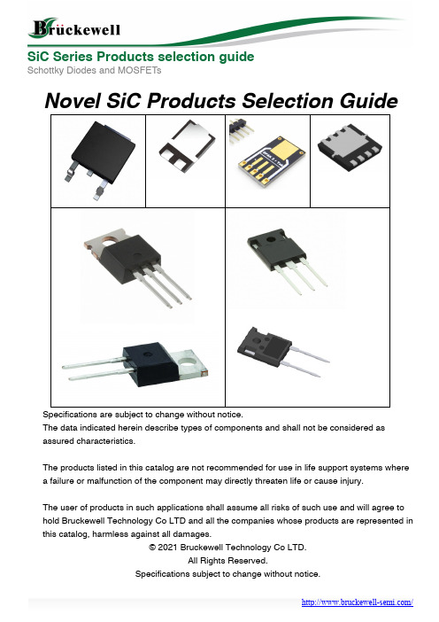
Schottky Diodes and MOSFETsNovel SiC Products Selection GuideSpecifications are subject to change without notice.The data indicated herein describe types of components and shall not be considered as assured characteristics.The products listed in this catalog are not recommended for use in life support systems where a failure or malfunction of the component may directly threaten life or cause injury.The user of products in such applications shall assume all risks of such use and will agree to hold Bruckewell Technology Co LTD and all the companies whose products are represented in this catalog, harmless against all damages.© 2021 Bruckewell Technology Co LTD.All Rights Reserved.Specifications subject to change without notice.Schottky Diodes and MOSFETsIn the recent decades, the Silicon carbide (SiC), turned out to be an excellent semiconductor material. Composed of carbon and silicon, and used in power applications in which it showed excellent performance,far superior to those of silicon.Significant progress has been made in the field of the semiconductor industry, in which the technologies forthe processing of silicon carbide have become increasingly more sophisticated, and have produced semiconductor devices with excellent performance.In the facts those devices during the applications have shown a remarkable capacity to reduce losses and ahigh switching speed in comparison to that offered by silicon. The use of silicon carbide (SiC) as a semiconductor begins to expand into multiple applications and always proves to be more and more the candidate to replace silicon in the most important applications such as automotive and E-Bike motor control.For these reasons, Bruckewell Semi decided to launch the production of the SiC Products, including the SiC Schottky Diode and SiC MOSFET, support the 650V to 1200V, and give the opportunity to its customers totake advantage of the benefits that the products offer in the SiC high-voltage power applications.Present our SiC products line as belowSMD PackageAmp DFN3X3 DFN5X6 TO-277 DFN 8X8 TO-252(DPak) TO-263(D2Pak)4 CBR04P65D6 CBR06P65HL CBR06P65D8 CBR08P65HL CBR08P65D10 CBR10P65HM CBR10P65SCBR10120SCBR10P65HLCBR10P65DCBR10120D20 CBR20120S30 CBR30120H CBR30120S40DFN 3X3 is unique package and CBR10P65HM is first smallest SiC SBD Diode in the industry.TO-277 has same foot print with TO-252 (DPak), and has better thermal performance.Through Hole PackageAmp TO-220AC TO-220AB TO-247 TO-247 (Dual Die)4 CBR04P656 CBR06P658 CBR08P6510 CBR10P65CBR10120 CBR10120PCBR10120W20 CBR20P65CBR20120CBR20P65PCCBR20120PCBR20P65WCBR20120WCBR20P65WCCBR20120WC30 CBR30120W40 CBR40P65WC CBR40120WCSchottky Diodes and MOSFETsPart NomenclatureExample: CBR20P65PC CBR SiC Barrier RectifierCMS SiC MOSFET20 IF, Forward current, as 20AP65 Breakdown Voltage, as P65=650V, 120=1200VPC Package CodeBlank: TO-220AC-2LP: TO-220ABPC: TO-220AB, Dual Die D: TO-252-2L, DPAKW: TO-247-2LWC: TO-247-3L, Dual Die WU: TO-247-3L, Single Die S: TO-277A: SMA, B: SMB, C: SMC B: TO-263, D2PAKH: DFN5x6HM: DFN3x3HL: DFN8x8When the diodes are used simultaneously:ΔTj(diode1) = P(diode1) x Rth(j-c) (per diode) + P(diode2) x Rth(c)To evaluate the conduction losses use the following equation:P = 1.35 x IF(AV) + 0.144 x IF2(RMS)Schottky Diodes and MOSFETsComparison with industry supplier-TO-220AC/ABAmpBruckewellST-MicroInfineonTO-220ACTO-220ABTO-220ACTO-220ABTO-220AC TO-220AB2 IDH02G65C5IDH02G120C53 IDH03SG60C IDH03G65C5 4CBR04P65IDH04SG60C IDH04G65C55 IDH05SG60C IDH05G65C5 IDH05G120C56 CBR06P65 STPSC6TH13TI IDH06SG60C IDH06G65C58 CBR08P65STPSC8TH13TI STPSC8H065CIDH08SG60C IDH08G65C5 IDH08G120C5 9IDH09SG60C IDH09G65C510CBR10P65 CBR10120CBR10120PSTPSC10H065D STPSC10H12D STPSC10TH13TIIDH10SG60CIDH10G65C5 IDH10G120C512 STPSC12065 STPSC1206 STPSC12H065CIDH12SG60C IDH12G65C515 STPSC15H1216STPSC16H065C IDH16G65C5IDH16G120C520CBR20P65 CBR20120CBR20P65PC CBR20120PSTPSC20065D STPSC20H12DSTPSC20H065CIDH20G65C5 IDH20G120C5Note:The suffix C5 in the Infineon Parts means the CoolSiC™ 5G, others are CoolSiC™ 3GSchottky Diodes and MOSFETsComparison with Japan suppliers-TO-220AC/ABAmpBruckewell Rohm Toshiba TO-220AC TO-220AB TO-220AC ITO-220AC TO-220AC ITO-220AC4 CBR04P65 SCS304AP TRS4E65F TRS4A65F5 SCS205KG6 CBR06P65 SCS306APSCS206AGSCS206AM TRS6E65F TRS6A65F8 CBR08P65 SCS308APSCS208AGSCS208AM TRS8E65F TRS8A65F10 CBR10P65CBR10120 CBR10120PSCS310APSCS210AGSCS210KGSCS210AM TRS10E65F TRS10A65F12 SCS212AG SCS212AM15 SCS215AGSCS215KGSCS215AM20 CBR20P65CBR20120CBR20P65PCCBR20120PSCS220AGSCS220KGSCS220AMNote:The suffix of Rohm Parts means the breakdown voltage, A means 650V, K means 1200VSchottky Diodes and MOSFETsComparison with industry supplier-TO-247 Single/ Dual DieAmpBruckewellST-MicroInfineonTO-247 TO-247 DualTO-247TO-247 DualTO-247TO-247 Dual 10 CBR10120WIDW10G65C5 IDW10G120C5B 20 CBR20P65W CBR20120W CBR20P65WC CBR20120WC STPSC20065WSTPSC20H065CWIDW20G65C5IDW20G65C5B IDW20G120C5B12 IDW12G65C515IDW15G120C5B16 IDW16G65C524IDW24G65C5B 30 CBR30120WIDW30G65C5IDW30G120C5B 32IDW32G65C5B 40CBR40120WCSTPSC40065CWIDW40G65C5IDW40G65C5B IDW40G120C5BComparison with Japan suppliers-TO-247 Single/ Dual DieAmpBruckewellRohmFuji electricTO-247 TO-247 DualTO-247TO-247 Dual TO-247 TO-247 Dual10 CBR10120WSCS210KE2FDCY10S6515SCS215AE20 CBR20P65W CBR20120W CBR20P65WC CBR20120WCSCS220AESCS220AE2 SCS220KE2FDCY18S120 FDCY20C6525 FDCY25S6530 CBR30120WSCS230AE2 SCS230KE240 CBR40120WCSCS240AE2 SCS240KE2FDCY36C120 50FDCY50C65Schottky Diodes and MOSFETsProduct IO(A)VB min (V)VF typ(V)IR Max (uA)PackageNumber of Diodes CBR04P65 4 650 1.5 10 TO-220AC 1 CBR04P65D 4 650 1.5 10 DPAK (TO-252) 1 CBR06P65 6 650 1.5 10 TO-220AC 1 CBR06P65D 6 650 1.5 10 DPAK (TO-252) 1 CBR 06P65HL 6 650 1.5 10 DFN 8X8 1 CBR08P65 8 650 1.5 10 TO-220AC 1 CBR08P65D 8 650 1.5 10 DPAK (TO-252) 1 CBR08P65HL 8 650 1.5 10 DFN 8X8 1 CBR10P65 10 650 1.5 10 TO-220AC 1 CBR10P65D 10 650 1.5 10 DPAK (TO-252) 1 CBR10P65S 10 650 1.5 10 TO-277 1 CBR10P65HM 10 650 1.5 10 DFN3.3 1 CBR10P65HL 10 650 1.5 10 DFN8X8 1 CBR20P65PC 20 650 1.5 10 TO-220AB 2 CBR20P65 20 650 1.5 10 TO-220AC 1 CBR20P65W 20 650 1.5 10 TO-247 1 CBR20P65WC 20 650 1.5 10 TO-247 2 CBR40P65WC 40 650 1.5 10 TO-247 2 CBR10120 10 1200 1.5 10 TO-220AC 1 CBR10120P 10 1200 1.5 10 TO-220AB 1 CBR10120D 10 1200 1.5 10 DPAK (TO-252) 1 CBR10120S 10 1200 1.5 10 TO-277 1 CBR10120W 10 1200 1.5 10 TO-247 1 CBR20120WC 20 1200 1.5 10 TO-247 2 CBR20120W 20 1200 1.5 10 TO-247 1 CBR20120 20 1200 1.5 10 TO-220AC 1 CBR20120P 20 1200 1.5 10 TO-220AB 1 CBR20120PC 20 1200 1.5 10 TO-220AB 2 CBR20120S 20 1200 1.5 10 TO-277 1 CBR30120W 30 1200 1.5 10 TO-247 1 CBR30120S 30 1200 1.5 10 TO-277 1 CBR30120H 30 1200 1.5 10 DFN 5X6 1 CBR40120WC 4012001.510 TO-2472Schottky Diodes and MOSFETsDisclaimerALL PRODUCT, PRODUCT SPECIFICATIONS AND DATA ARE SUBJECT TO CHANGE WITHOUT NOTICE TO IMPROVE RELIABILITY, FUNCTION OR DESIGN OR OTHERWISE. Bruckewell Technology Inc., its affiliates, agents, and employees, and all persons acting on its or their behalf (collectively, “Bruckewell”), disclaim any and all liability for any errors, inaccuracies or incompleteness contained in any datasheet or in any other disclosure relating to any product. Bruckewell makes no warranty, representation or guarantee regarding the suitability of the products for any particular purpose or the continuing production of any product. To the maximum extent permitted by applicable law, Bruckewell disclaims(i) Any and all liability arising out of the application or use of any product.(ii) Any and all liability, including without limitation special, consequential or incidental damages. (iii) Any and all implied warranties, including warranties of fitness for particular purpose, non-infringement and merchantability.Statements regarding the suitability of products for certain types of applications are based on Bruckewell’s knowledge of typical requirements that are often placed on Bruckewell products in generic applications.Such statements are not binding statements about the suitability of products for a particular application. It is the customer’s responsibility to validate that a particular product with the properties described in the product specification is suitable for use in a particular application. Parameters provided in datasheets and/or specifications may vary in different applications and performance may vary over time.Product specifications do not expand or otherwise modify Bruckewell’s terms and conditions of purchase, including but not limited to the warranty expressed therein.。
- 1、下载文档前请自行甄别文档内容的完整性,平台不提供额外的编辑、内容补充、找答案等附加服务。
- 2、"仅部分预览"的文档,不可在线预览部分如存在完整性等问题,可反馈申请退款(可完整预览的文档不适用该条件!)。
- 3、如文档侵犯您的权益,请联系客服反馈,我们会尽快为您处理(人工客服工作时间:9:00-18:30)。
Fig. 4 Non-Repetitive Peak Forward Surge Current (Pulse Mode)
Fig. 5 Power Derating
Fig. 6 Current Derating
09 / 10
SiC Schottky Diode
S2D065V010E
Package TO-252-2L Inner Circuit Product Summary
更高的 电能转换效率
更高的 工作温度
更高的 工作频率
更小的 体积和体重
SiC Schottky Diode
S2D065V010A
Package TO-220-2L Inner Circuit Product Summary
S2D065V010A�
Maximum Ratings
VR IF QC
650 V 12A 10A
(Tc= 135 ℃ ) (Tc= 145 ℃ )
Parameter
Symbol
Test Conditions
TC = 25℃, TP = 10 ms Half Sine Wave
Value
on-Repetitive Peak Forward Surge Current I FSM
Benefits
u u u u u u Higher System Efficiency Parallel Device Convenience High Temperature Application High Frequency Operation Hard Switching & High Reliability Environmental Protection Power Dissipation PD TJ Tstg RΘJC Repetitive Peak Forward Surge Current I FRM
S2D065V010E
Package Dimensions TO-252-2L
Fig. 1 Forward Characteristics
Fig. 2 Reverse Characteristics
Fig. 3 Capacitance vs. Reverse Voltage
Fig. 4 Power Derating
QC
Continuous Forward Current
Total Capacitance
C
V R=200V, TJ=25 ℃ , f =1 MHz V R=400V, TJ=25 ℃ , f =1 MHz
pF
11 / 12
SiC Schottky Diode
S2D065V010E
Device Performances
Non-Repetitive Peak Forward Surge Current I FSM
TC = 125℃, TP = 10 ms Half Sine Wave TC = 25℃, TP = 10 µ s Pulse TC = 25℃, TP = 10 ms
55
A
TBD
A
Features
u u u u u u Low Conduction and Switching Loss Positive Temperature Coefficient on V F Temperature Independent Switching Behavior Fast Reverse Recovery High Surge Current Capability Pb-free lead plating
Symbol
V RRM V RSM VR IF
Test Conditions
TJ = 25℃ TJ = 25℃ TJ = 25℃ TC= 25℃ TC= 135℃ TC= 141℃
Value
650 650 650 24 11 10
Unit
V V V A A A
Reverse Current
IR
Total Capacitive Charge
S2D065V010A
Device Performances
S2D065V010A�
Package Dimensions TO-220-2L
Fig. 1 Forward Characteristics
Fig. 2 Reverse Characteristics
Fig. 3 Capacitance vs. Reverse Voltage
Fig. 5 Current Derating
13 / 14
SiC Schottky Diode
S2D065V010G
Package TO-263-2L Inner Circuit Product Summary
QC
Continuous Forward Current
IF
TC = 135 ℃ TC = 145 ℃
Total Capacitance
C
V R=200V, TJ=25 ℃ , f =1 MHz V R=400V, TJ=25 ℃ , f =1 MHz
pF
07 / 08
SiC Schottky Diode
Half Sine Wave, D = 0.1 TC = 125℃, TP = 10 ms Half Sine Wave, D = 0.1 TC = 25℃ TC = 125℃
33
A
25 79 26 175 -55 to 175 1.9
A W W ℃ ℃ ℃/W
Operating Junction and Storage Temperature Thermal Resistance Junction to Case
Symbol
V RRM V RSM VR
Test Conditions
TJ = 25 ℃ TJ = 25 ℃ TJ = 25 ℃ TC = 25 ℃
Value
650 650 650 26 12 10
Unit
V V V A A A
Reverse Current
IR
Total Capacitive Charge
V DC VF
Test Conditions
I R = 100 µA, TJ = 25 ℃ I F = 10A, TJ = 25 ℃ I F = 10A, TJ = 175 ℃ V R = 600V, TJ = 25 ℃ V R = 600V, TJ = 175 ℃ I F = 10A, dI/dt=300A/µs, V R=400V, TJ=25 ℃ V R=1V, TJ=25 ℃ , f =1 MHz
Typ.
> 650 1.5 1.9 <1 15 19 398 53 52
Max.
1.8 2.2 50 160
Unit
V V V µA µA nC
Maximum Ratings
Forward Voltage
Parameter
Peak Repetitive Reverse Voltage Peak Reverse Surge Voltage DC Blocking Voltage
Half Sine Wave, D = 0.1 TC = 125℃, TP = 10 ms Half Sine Wave, D = 0.1 TC = 25℃ TC = 125℃
51
A
46 88 29 175 -55 to 175 1.7
A W W ℃ ℃ ℃/W
Operating Junction and Storage Temperature Thermal Resistance Junction to Case
VC VF
Test Conditions
I R = 100 µA, TJ = 25 ℃ I F = 10A, TJ = 25 ℃ I F = 10A, TJ = 175 ℃ V R = 600V, TJ = 25 ℃ V R = 600V, TJ = 175 ℃ I F = 10A, dI/dt=300A/µs, V R=400V, TJ=25 ℃ V R=1V, TJ=25 ℃ , f =1 MHz
Applications
u u u SMPS PFC Solar/ Wind Renewable Energy u u u Power Inverters Motor Drives UPS
Electrical Characteristics
Parameter
DC Blocking Voltage
Symbol
Applications
u u u SMPS PFC Solar/ Wind Renewable Energy u u u Power Inverters Motor Drives UPS
Electrical Characteristics
Parameter
DC Blocking Voltage
Symbol
上海诺卫卡电子科技有限公司
邮编 Postcode:200000 电话 Tel:13717783997 邮箱 Fax:1023403651@
上海诺卫卡电子科技有限公司
上海诺卫卡电子科技有限公司是一家专业从事宽禁带半导体碳化硅衬底、外延、器件、设备、加 工耗材及相关产品的专业服务商,具有丰富的电子行业经验。 公司拥有国际化的管理团队和专业的运营团队,与众多国际知名半导体厂商建立了良好的合作关 系,竭诚为广大客户提供服务快捷、优质服务。 公司提供国际知名半导体厂商的宽禁带半导体碳化硅衬底、外延、器件、设备、加工耗材及相关 产品等产品; 公司也提供高品质莫桑钻原石及系列产品。 公司客户涵盖国内外主要大型半导体企业及应用厂商,秉承着“专业服务,客户第一”的宗旨, 与广大客户建立了良好的合作关系,获得了广泛的信誉与支持。 公司拥有专业、高效的售后服务团队,并与厂商充分合作,为广大客户提供全程、全方位的优质 服务。 我们期待着与您的合作,携手共创美好明天!