移位寄存器-功率-TI-tpic6b595
HM6B595

单位:英寸(毫米)
HM6B595DW
表面贴装式 (SOP-20)
单位:英寸(毫米)
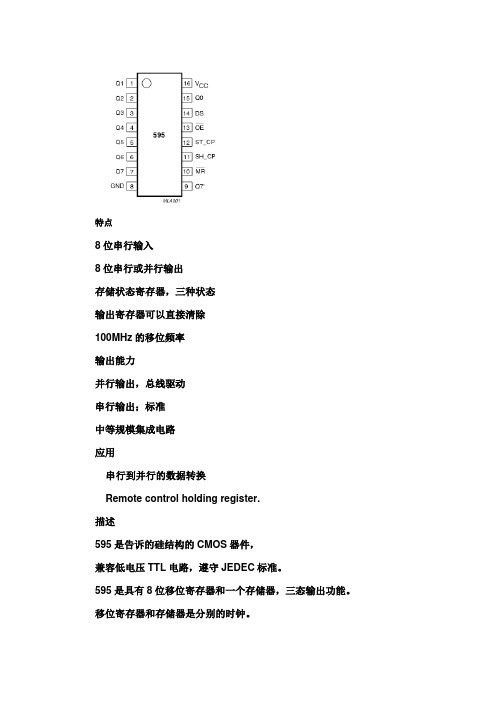
管脚次序 2 3 4--7 14--17 8 9 10, 11, 19 12 13 18 1, 20
符 号 VDD Sin 串行输入数据端.
管 电源端. 低压信息处理的电源.
脚
功
能
Q0--Q3 并行移位输出端. 输出移位寄存器或锁存器的数据. Q4--Q7 R OE GND STR CLK SOUT NC 复位端. 当复位端为低电平时, 移位寄存器被置”0”, 锁存器不受其影响. 输出使能端. 当使能端为低电平时, 锁存器内的数据被送至输出端. 当使能端 为高电平时, 输出端 Q0--Q7 变为高阻抗状态, 即截止态. 地线端. 选通端. 当 ST 脉冲前沿跳变时, 移位寄存器的数据进入到各锁存器. 移位寄存器时钟输入端. 当移位时钟脉冲前沿跳变时, 串行输入的数据被移入 到八位移位寄存器之中. 串行输出端. 移位时钟脉冲前沿跳变时输出第八位移位寄存器的数据. 空脚.
大屏幕显示驱动 LED 的专用电路 一 . 概述 HM6B595 由一个八位串入并出/串入串出移位寄存器, 八位数据锁存器和驱动器三个 主要部分构成. 移位寄存器接收串行输入数据, 输出串行数据, 并提供送往锁存器的并行 数据 . 移位寄存器和锁存器有独立的时钟输入端, 移位寄存器有异步的复位端. 本电路管 脚逻辑与 TPIC6B595 全兼容. 二 . 特点 1. 电源电压范围宽 , 输出驱动级采用集电极开路输出结构 , 工作电压 16V, 可直接驱动 LED 和继电器. 2. 信号端,时钟端带施密特整形, 提高抗干扰能力, 保证数据有效可靠. 3. 数据处理速度高, 电路采用 BiMOS 工艺, 串行最高时钟频率 f 不低于 10MHz. 4. 串行输出电流大, 便于直接级联. 5. 备有双列直插式 HM6B595N(DIP-20)及表面贴装式 HM6B595DW(SOP-20)两种封装. 三 . HM6B595N, HM6B595DW 引脚定义 ( 顶视 ) 及逻辑符号
595芯片管脚的作用
特点8位串行输入8位串行或并行输出存储状态寄存器,三种状态输出寄存器可以直接清除100MHz的移位频率输出能力并行输出,总线驱动串行输出;标准中等规模集成电路应用串行到并行的数据转换Remote control holding register.描述595是告诉的硅结构的CMOS器件,兼容低电压TTL电路,遵守JEDEC标准。
595是具有8位移位寄存器和一个存储器,三态输出功能。
移位寄存器和存储器是分别的时钟。
数据在SCHcp的上升沿输入,在STcp的上升沿进入的存储寄存器中去。
如果两个时钟连在一起,则移位寄存器总是比存储寄存器早一个脉冲。
移位寄存器有一个串行移位输入(Ds),和一个串行输出(Q7’),和一个异步的低电平复位,存储寄存器有一个并行8位的,具备三态的总线输出,当使能OE时(为低电平),存储寄存器的数据输出到总线。
参考数据符号参数条件TYP 单位HC HCttPHL/tPLH 传输延时SHcp到Q7’STcp到QnMR到Q7’CL=15pFVcc=5V161714 212019 NsNsNsfmax STcp到SHcp最大时钟速度10057 MHzCL 输入电容Notes 1 3.5 3.5 pFCPD Power dissipation capacitance per package. Notes2115 130 pFCPD决定动态的能耗,PD=CPD×VCC×f1+∑(CL×VCC2×f0)F1=输入频率,CL=输出电容f0=输出频率(MHz)Vcc=电源电压引脚说明符号引脚描述Q0…Q7 15,1,7 并行数据输出GND 8 地Q7’ 9 串行数据输出MR 10 主复位(低电平)SHCP 11 移位寄存器时钟输入STCP 12 存储寄存器时钟输入OE 13 输出有效(低电平)DS 14 串行数据输入VCC 16 电源功能表输入输出功能SHCP STCP O E MR DS Q7’ Qn× × L ↓ × L NC MR为低电平时紧紧影响移位寄存器× ↑ L L × L L 空移位寄存器到输出寄存器× × H L × L Z 清空移位寄存器,并行输出为高阻状态↑ × L H H Q6’ NC 逻辑高电平移入移位寄存器状态0,包含所有的移位寄存器状态移入,例如,以前的状态6(内部Q6”)出现在串行输出位。
放大器模块常用芯片简介
放大器模块常用芯片简介MAX4106:⑴低成本,高速,单电源运算放大器。
⑵满摆幅输出的运算放大器,-3db带宽为150MHZ,可以采用正负5V或者单电源供电,⑶采用Umax-8和SO-8封装。
THS3092:⑴高速电流反馈双运算放大器芯片⑵160MHZ(G=5,RL=100)电源电源范围正负5-15V. ⑶采用SOIC-8和TSSOP-14封装。
AD624:⑴高精度,低噪声仪表放大器芯片⑵主要用于设计低电平传感器(负荷传感器,应变计和压力传感器)⑶可用于高速数据采集应用。
AD603⑴90MHZ带宽,增益程控可调的集成运算放大器芯片⑵增益与控制电压成线性关系,增益变化范围40dB ⑶采用SOIC-8和CERDIP-8封装AD8055;⑴电压反馈型放大器芯片⑵该芯片0.1dB增益平坦度为40MHZ,带宽达300MHZ,压摆率为1400V/us,建立时间为20ns,适合各种高速应用。
⑶采用正负5V双电源或+12V单电源,仅需5mA的电源电流,负载电流可达60mA,工作温度-40―+125度。
⑷采用PDIP-8,SOIC-8和SOT-23-5封装 AD811⑴视频运算放大器芯片⑵具有高速,高频,宽频带和低噪声等优异特性⑶具有140MHZ带宽,120MHZ带宽,35MHZ带宽,2500V/us摆率,建立时间25ns⑷采用8引脚SOIC(R-8),16,20引脚等ICL7650/53: ⑴运算放大器芯片⑵具有极低的输入失调电压,整个工作温度范围(约100度)内只有1Uv,失调电压的温漂为0.01Uv/度,开环增益极高,转换率SR=2.5V/us………⑶电源电压范围V+到V-为4.5-16V.LM386⑴音频功率放大器⑵工作电压4-12V,5-18V静态功耗约4mA可用于电池供电,电压增益范围20-200,可调;⑶采用8引线双列直插式,贴片式封装 TEA2050⑴双声道立体声音频功率放大集成电路芯片⑵工作电源电压3-15V,工作电压6-9V,输出功率与电源电压和扬声器阻抗有关⑶采用POWERDIP16和SO20封装 LTC1068⑴开关电容滤波器芯片⑵它包含4个同样的二阶滤波器。
英飞凌 ICE5xSAG 第五代固定频率PWM控制器 数据表

ICE5xSAG采用 DSO-8 封装的固定频率 PWM 控制器产品亮点• 可选进入和退出待机功率电平的增强型主动突发模式,其最低待机功率小于 100 mW• 数字降频模式,提高整体系统效率 • 借助共源共栅配置实现快速启动 • 支持频率抖动和软栅极驱动,实现低 EMI • 集成误差放大器• 具备交流输入过压保护,提供全面防护 • 无铅电镀、无卤模塑化合物,符合 RoHS 标准特性• 可选进入和退出待机功率电平的增强型主动突发模式• 数字频率降低,提高整体系统效率 • 借助共源共栅配置实现快速启动• 支持 DCM (非连续导通模式)和 CCM (连续导通模式)运行,具备斜坡补偿• 支持频率抖动和软栅极驱动,实现低 EMI • 内置数字软启动• 集成误差放大器,在非隔离反激式架构中支持直接(原边)反馈• 具备交流输入过压保护、V CC 过压、V CC 欠压、过载/开路及过温保护机制,提供全面防护• 所有保护功能均处于自动重启模式 • 受限的V CC 短接至地的充电电流应用• 适用于家用电器/白色家电、电视、电脑及服务器的辅助电源• 蓝光播放器、机顶盒和 LCD/LED 显示器产品验证完全符合 JEDEC 工业应用标准要求描述ICE5xSAG 是第五代固定频率 PWM 控制器,支持共源共栅配置,并针对离线开关模式电源进行了优化。
其共源共栅配置亦可实现快速启动。
器件通过降低频率并软化栅极驱动和频率抖动,进而在低负载和 50% 负载之间实现低 EMI 效果,并提高了效率。
产品支持主动突发模式,可选进入和退出待机功率,输出电压纹波小且可控,因此可在待机模式下具备较高的灵活性和极低功耗。
此外, ICE5xSAG 有宽的供电电压工作范围 (10.0~25.5 V),功耗较低。
产品具备诸多保护功能,提供可调交流输入过压保护,可在故障情况下为电源系统提供全面防护。
凭借上述特性,第五代 ICE5xSAG 系列得以成为市面上用于固定频率反激式转换器的理想 PWM 控制器。
74HC595PW TI运算放大器
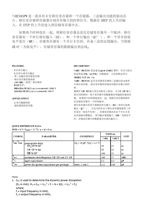
74HC595PW 是一款具有8位移位寄存器和一个存储器,三态输出功能的驱动芯片。
移位寄存器和存储器分别具有独立的时钟信号。
数据在SHCP 的上升沿输入,在STCP 的上升沿进入到存储寄存器中去。
如果两个时钟连在一起,则移位寄存器总是比存储寄存器早一个脉冲。
移位寄存器有一个串行移位输入(DS ),和一个串行输出(Q7’),和一个异步的低电平复位(MR ),存储寄存器有一个并行8位的,具备三态的总线输出,当使能OE 时(为低电平),存储寄存器的数据输出到总线。
FEATURES · 8位串行输入 · 8位串行或并行输出 · 带三态输出的存储寄存器 · 移位寄存器直接清除 · 100 MHz (典型)移出频率 · ESD 防护:HBM EIA/JESD22-A114-A exceeds 2000 V MM EIA/JESD22-A115-A exceeds 200 V.APPLICATIONS · S 串并数据转换 · 遥控器保持寄存器。
QUICK REFERENCE DATAGND = 0 V; T amb = 25 ︒C; t r = t f = 6 ns.DESCRIPTION74HC / HCT595是高速Si-gate CMOS 器件,并且与低功耗肖特基TTL (LSTTL )引脚兼容。
它们的指定符合JEDEC 标准No. 7A 。
74HC / HCT595是具有存储寄存器和三态输出的8级串行移位寄存器。
移位寄存器和存储寄存器具有独立的时钟。
数据在SH_CP 输入的正向跃迁上移动。
在ST_CP 输入的正向转换时,每个寄存器中的数据都会传输到存储寄存器。
如果两个时钟都连接在一起,则移位寄存器将始终比存储寄存器早一个时钟脉冲。
移位寄存器具有用于级联的串行输入(DS )和串行标准输出(Q7’)。
它还为所有8个移位寄存器级提供了异步复位(低电平有效)。
HC595完整中文资料

HC595完整中⽂资料74HC595芯⽚是⼀种串⼊并出的芯⽚,在电⼦显⽰屏制作当中有⼴泛的应⽤。
74HC595是8位串⾏输⼊/输出或者并⾏输出移位寄存器,具有⾼阻、关、断状态。
三态。
特点 8位串⾏输⼊ 8位串⾏或并⾏输出存储状态寄存器,三种状态输出寄存器可以直接清除 100MHz的移位频率输出能⼒并⾏输出,总线驱动串⾏输出;标准中等规模集成电路应⽤串⾏到并⾏的数据转换 Remote contr ol holding register. 描述 595是告诉的硅结构的CMOS器件,兼容低电压TTL电路,遵守JEDEC标准。
595是具有8位移位寄存器和⼀个存储器,三态输出功能。
移位寄存器和存储器是分别的时钟。
数据在SCHcp的上升沿输⼊,在STcp 的上升沿进⼊的存储寄存器中去。
如果两个时钟连在⼀起,则移位寄存器总是⽐存储寄存器早⼀个脉冲。
移位寄存器有⼀个串⾏移位输⼊(Ds),和⼀个串⾏输出(Q7’),和⼀个异步的低电平复位,存储寄存器有⼀个并⾏8位的,具备三态的总线输出,当使能OE时(为低电平),存储寄存器的数据输出到总线。
CPD决定动态的能耗, PD=CPD×VCC×f1+∑(CL×VCC2×f0) F1=输⼊频率,CL=输出电容 f0=输出频率(MHz) Vcc=电源电压引脚说明符号引脚描述内部结构结合引脚说明就能很快理解 595的⼯作情况引脚功能表:真值表:1)74164和74595功能相仿,都是8位串⾏输⼊转并⾏输出移位寄存器。
74164的驱动电流(25mA)⽐74595(35mA)的要⼩,14脚封装,体积也⼩⼀些。
2)74595的主要优点是具有数据存储寄存器,在移位的过程中,输出端的数据可以保持不变。
这在串⾏速度慢的场合很有⽤处,数码管没有闪烁感。
与164只有数据清零端相⽐,595还多有输出端时能/禁⽌控制端,可以使输出为⾼阻态。
3)595是串⼊并出带有锁存功能移位寄存器,它的使⽤⽅法很简单,在正常使⽤时SCLR为⾼电平, G为低电平。
硬件设计说明书

硬件设计说明书一、设计概要本产品主要基于《滴滴标准化电池产品规格书V1.0》《滴滴电池场景和充放电流程图说明》《滴滴电池底仓和NFC的透传协议》等技术规格书设计而成。
满足产品功能需求,具有市场竞争力。
二、BMS功能框图三、功能设计详解1、电源设计①DC-DC设计电源芯片使用TI的LM5164,该芯片具有超低 IQ,100V输入、1A 同步降压直流/直流转换器;空载输入静态电流:10.5µA;关断静态电流:3µA,用以在休眠时降低系统功耗。
电路图如下所示:②LDO设计电源芯片采用TI的TLV70433和TLV70450,分别输出3.3V电源和5V电源。
3.3V电源为BMS系统供电,5V为CAN通信电源供电。
电路如下图所示:另外,部分外设电源采用3V3_Com供电,在休眠状态下关闭3V3_Com,降低功耗。
电路如下图所示:2、主回路设计本产品主回路采用高端驱动的方式,驱动芯片采用TI的BQ76200PWR(bq76200 高压电池组前端充电/放电高侧NFET 驱动器),驱动信号使用中颖的SH367309。
CHG信号控制充电MOS,DCHG信号控制放电MOS,PDCHG 信号控制预充电路。
预充电路如下图所示:主MOS管采用美格纳的MDE1991,Vds最高可达118V,RDS(ON) < 4.4 mΩ @VGS = 10V。
驱动电路和主回路如下图所示3、电压采集,电流采集,温度采集,均衡电路设计前端采集芯片采用中颖的SH367309,13bit VADC用于采集电压/温度/电流/均衡/保护等功能。
采集电路和外围参数配置如下图所示:其中,使用SH367309采集3路电芯温度。
并留有烧写接口。
4、单片机及外围电路设计单片机采用ST的STM32F072RBT6(ARM®-based 32-bit MCU, up to 128 KB Flash,crystal-less USB FS 2.0,CAN,12 timers, ADC,DAC & comm.interfaces,2.0 - 3.6 V)。
74HC595使用笔记

注:SH_CP 输出脉冲与 ST_CP 输出脉冲互不影响,是两个独立的过程,即:可以一边进行数据移 位,一边数据输出,可以同时进行。这是此芯片的优点,在移位的过程中,输出端数据可以保持不变。 在串行速度较慢的数码管应用时,可以利用这个特点,减轻数码管的闪烁。
6.软件代码(未级联)
//宏定义
#define
74HC595(74HCT595)芯片使用笔记
作者:无明 mmdmmyx@ 201503
1.简介 74HC595(74HCT595),是 8-bit 串行输入,实现 8-bit 串行或并行输出,带有移位寄存器和输出
锁存,输出端口带有三态功能; 芯片封装形式有:DIP16、SO16、SSOP16、TSSOP16、DHVQFN16。引脚控制信号可以IO口模拟,也
用时可根据要移位的数据位数,发出相应数量的脉冲数; PIN12(ST_CP):存储寄存器的时钟输入,上升沿时移位寄存器的数据进入数据存储寄存器,下降
沿时存储寄存器数据不变,即当上升沿时,Q0-Q7 按照当前移位寄存器数据进行并行输出;(例:设 输入数据为 0x01,①在每一次移位后,ST_CP 都发出脉冲,则可实现 8 个通道的循环选通;②在所有 移位完成后(SH_CP 脉冲完成),ST_CP 发出脉冲,可实现 8 个通道选通第 1 通道,如此将 0x01 更换 为不同的输入数据,可以实现不同的 1 个或多个通道的并行输出);
for(i=0;i<8;i++) {
if( (uc74595data & 0x01) == 0 ) {
SIO_IN_LOW; } else {
SIO_IN_HIGH; } SIO_CLK_LOW; uc74595data = uc74595data>>1; _nop_( ); _nop_( ); _nop_( ); _nop_( ); _nop_( ); SIO_CLK_HIGH; _nop_( ); } SIO_LATCH_LOW; SIO_CLK_LOW; _nop_( ); _nop_( ); _nop_( ); _nop_( ); SIO_LATCH_HIGH; _nop_( );
- 1、下载文档前请自行甄别文档内容的完整性,平台不提供额外的编辑、内容补充、找答案等附加服务。
- 2、"仅部分预览"的文档,不可在线预览部分如存在完整性等问题,可反馈申请退款(可完整预览的文档不适用该条件!)。
- 3、如文档侵犯您的权益,请联系客服反馈,我们会尽快为您处理(人工客服工作时间:9:00-18:30)。
PACKAGING INFORMATIONOrderable Device Status (1)Package Type Package Drawing Pins Package Qty Eco Plan (2)Lead/Ball Finish MSL Peak Temp (3)TPIC6B595DW ACTIVE SOIC DW 2025TBD CU NIPDAU Level-1-220C-UNLIM TPIC6B595DWG4ACTIVE SOIC DW 2025Green (RoHS &no Sb/Br)CU NIPDAU Level-1-260C-UNLIM TPIC6B595DWR ACTIVE SOIC DW 202000TBDCU NIPDAU Level-1-220C-UNLIM TPIC6B595DWRG4ACTIVE SOIC DW 202000Green (RoHS &no Sb/Br)CU NIPDAU Level-1-260C-UNLIM TPIC6B595NACTIVEPDIPN2020Pb-Free (RoHS)CU NIPDAUN /A for Pkg Type(1)The marketing status values are defined as follows:ACTIVE:Product device recommended for new designs.LIFEBUY:TI has announced that the device will be discontinued,and a lifetime-buy period is in effect.NRND:Not recommended for new designs.Device is in production to support existing customers,but TI does not recommend using this part in a new design.PREVIEW:Device has been announced but is not in production.Samples may or may not be available.OBSOLETE:TI has discontinued the production of the device.(2)Eco Plan -The planned eco-friendly classification:Pb-Free (RoHS),Pb-Free (RoHS Exempt),or Green (RoHS &no Sb/Br)-please check /productcontent for the latest availability information and additional product content details.TBD:The Pb-Free/Green conversion plan has not been defined.Pb-Free (RoHS):TI's terms "Lead-Free"or "Pb-Free"mean semiconductor products that are compatible with the current RoHS requirements for all 6substances,including the requirement that lead not exceed 0.1%by weight in homogeneous materials.Where designed to be soldered at high temperatures,TI Pb-Free products are suitable for use in specified lead-free processes.Pb-Free (RoHS Exempt):This component has a RoHS exemption for either 1)lead-based flip-chip solder bumps used between the die and package,or 2)lead-based die adhesive used between the die and leadframe.The component is otherwise considered Pb-Free (RoHS compatible)as defined above.Green (RoHS &no Sb/Br):TI defines "Green"to mean Pb-Free (RoHS compatible),and free of Bromine (Br)and Antimony (Sb)based flame retardants (Br or Sb do not exceed 0.1%by weight in homogeneous material)(3)MSL,Peak Temp.--The Moisture Sensitivity Level rating according to the JEDEC industry standard classifications,and peak solder temperature.Important Information and Disclaimer:The information provided on this page represents TI's knowledge and belief asof the date that it is provided.TI bases its knowledge and belief on information provided by third parties,and makes no representation or warranty as to the accuracy of such information.Efforts are underway to better integrate information from third parties.TI has taken and continues to take reasonable steps to provide representative and accurate information but may not have conducted destructive testing or chemical analysis on incoming materials and chemicals.TI and TI suppliers consider certain information to be proprietary,and thus CAS numbers and other limited information may not be available for release.In no event shall TI's liability arising out of such information exceed the total purchase price of the TI part(s)at issue in this document sold by TI to Customer on an annual basis.PACKAGE OPTION ADDENDUM29-May-2007Addendum-Page 1IMPORTANT NOTICETexas Instruments Incorporated and its subsidiaries(TI)reserve the right to make corrections,modifications,enhancements,improvements, and other changes to its products and services at any time and to discontinue any product or service without notice.Customers should obtain the latest relevant information before placing orders and should verify that such information is current and complete.All products are sold subject to TI’s terms and conditions of sale supplied at the time of order acknowledgment.TI warrants performance of its hardware products to the specifications applicable at the time of sale in accordance with TI’s standard warranty.Testing and other quality control techniques are used to the extent TI deems necessary to support this warranty.Except where mandated by government requirements,testing of all parameters of each product is not necessarily performed.TI assumes no liability for applications assistance or customer product design.Customers are responsible for their products and applications using TI components.To minimize the risks associated with customer products and applications,customers should provide adequate design and operating safeguards.TI does not warrant or represent that any license,either express or implied,is granted under any TI patent right,copyright,mask work right, or other TI intellectual property right relating to any combination,machine,or process in which TI products or services are rmation published by TI regarding third-party products or services does not constitute a license from TI to use such products or services or a warranty or endorsement e of such information may require a license from a third party under the patents or other intellectual property of the third party,or a license from TI under the patents or other intellectual property of TI.Reproduction of TI information in TI data books or data sheets is permissible only if reproduction is without alteration and is accompanied by all associated warranties,conditions,limitations,and notices.Reproduction of this information with alteration is an unfair and deceptive business practice.TI is not responsible or liable for such altered rmation of third parties may be subject to additional restrictions.Resale of TI products or services with statements different from or beyond the parameters stated by TI for that product or service voids all express and any implied warranties for the associated TI product or service and is an unfair and deceptive business practice.TI is not responsible or liable for any such statements.TI products are not authorized for use in safety-critical applications(such as life support)where a failure of the TI product would reasonably be expected to cause severe personal injury or death,unless officers of the parties have executed an agreement specifically governing such use.Buyers represent that they have all necessary expertise in the safety and regulatory ramifications of their applications,and acknowledge and agree that they are solely responsible for all legal,regulatory and safety-related requirements concerning their products and any use of TI products in such safety-critical applications,notwithstanding any applications-related information or support that may be provided by TI.Further,Buyers must fully indemnify TI and its representatives against any damages arising out of the use of TI products in such safety-critical applications.TI products are neither designed nor intended for use in military/aerospace applications or environments unless the TI products are specifically designated by TI as military-grade or"enhanced plastic."Only products designated by TI as military-grade meet military specifications.Buyers acknowledge and agree that any such use of TI products which TI has not designated as military-grade is solely at the Buyer's risk,and that they are solely responsible for compliance with all legal and regulatory requirements in connection with such use. TI products are neither designed nor intended for use in automotive applications or environments unless the specific TI products are designated by TI as compliant with ISO/TS16949requirements.Buyers acknowledge and agree that,if they use any non-designated products in automotive applications,TI will not be responsible for any failure to meet such requirements.Following are URLs where you can obtain information on other Texas Instruments products and application solutions:Products ApplicationsAmplifiers AudioData Converters AutomotiveDSP BroadbandClocks and Timers Digital ControlInterface MedicalLogic MilitaryPower Mgmt Optical NetworkingMicrocontrollers SecurityRFID TelephonyRF/IF and ZigBee®Solutions Video&ImagingWirelessMailing Address:Texas Instruments,Post Office Box655303,Dallas,Texas75265Copyright©2008,Texas Instruments Incorporated。