Positive magnetoresistance and orbital ordering in La(1-x)Sr(x)MnO(3)
Zero-gap materials零能隙材料
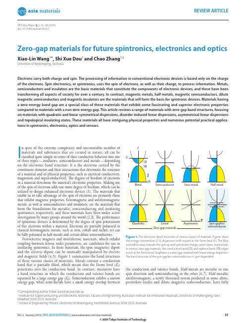
REVIEW ARTICLENPG Asia Mater. 2(1) 31–38 (2010)doi: 10.1038/asiamat.2010.7In spite of the extreme complexity and uncountable number of materials and substances that are created in nature, all can be classifi ed quite simply in terms of their conductive behavior into one of three types — insulators, semiconductors and metals — depending on the electronic band structure. It is the electrons carried by the constituent elements and their interactions that determine the structure of a material and its physical properties, such as electrical conductivity, magnetism and superconductivity. Th e degrees of freedom of electrons in a material determine the material’s electronic properties. Making use of the spin of electrons adds one more degree of freedom, which can be utilized to design enhanced electronic devices [1]. The materials that enable us to take advantage of the spin of electrons are primarily those that exhibit magnetic properties. Ferromagnetic and antiferromagnetic metals, as well as semiconductors and insulators, are the materials that form the foundations for metallic, semiconducting and insulating spintronics, respectively, and these materials have been under active investigation by many groups around the world [2,3]. Th e performance of spintronic devices is determined by the degree of spin polarization of free electrons within a material. Electrons are partially polarized in classical ferromagnetic metals, such as iron, cobalt and nickel, yet can be fully polarized in half-metals and certain dilute semiconductors.Ferroelectric magnets and multiferroic materials, which exhibit coupling between ferroic order parameters, are candidates for use in insulating spintronics. In these materials, the spin (magnetic) dipole and the electric dipole can be mutually manipulated by electric and magnetic fields [4,5]. Figure 1 summarizes the band structures of these various classes of materials. Metals contain a conduction band that is partially filled, which means that the Fermi level (E f ) penetrates into the conduction band. In contrast, insulators have a band structure in which the conduction and valence bands are separated by a large energy gap (E g ). Semiconductors exhibit a narrow energy gap, while semi-metals have a small energy overlap betweenthe conduction and valence bands. Half-metals are metallic in one spin direction and semiconducting in the other [6,7]. Half-metallic antiferromagnets, a newly theorized system predicted in some alloys, perovskite oxides and dilute magnetic semiconductors, have fullyZero-gap materials for future spintronics, electronics and opticsXiao-Lin Wang 1*, Shi Xue Dou 1 and Chao Zhang 1,2University of Wollongong, AustraliaElectrons carry both charge and spin. The processing of information in conventional electronic devices is based only on the charge of the electrons. Spin electronics, or spintronics, uses the spin of electrons, as well as their charge, to process information. Metals, semiconductors and insulators are the basic materials that constitute the components of electronic devices, and these have been transforming all aspects of society for over a century. In contrast, magnetic metals, half-metals, magnetic semiconductors, dilute magnetic semiconductors and magnetic insulators are the materials that will form the basis for spintronic devices. Materials having a zero-energy band gap are a special class of these materials that exhibit some fascinating and superior electronic properties compared to materials with a non-zero energy gap. This article reviews a range of materials with zero-gap band structures, focusing on materials with quadratic and linear symmetrical dispersions, disorder-induced linear dispersions, asymmetrical linear dispersions and topological insulating states. These materials all have intriguing physical properties and numerous potential practical applica-tions in spintronics, electronics, optics and sensors.*Corresponding author. Email: xiaolin@.au 1Institute for Superconducting and Electronic Materials, Faculty of Engineering, Australian Institute for Innovative Materials, University of Wollongong, Fairy Meadow, NSW 2519, Australia 2School of Engineering Physics, University of Wollongong, Northfi elds Avenue, NSW 2522, AustraliaFigure 1. The electronic band structures of various classes of materials. Figures show the energy–momentum (E –k ) dispersions with respect to the Fermi level (E f ). The blue and yellow areas indicate the spin-up and spin-down charge carrier states, respectively. In intrinsic zero-gap materials, the conduction band (CB) and valence band (VB) edges touch at the Fermi level. Graphene is a zero-gap material with linear energy dispersion. The band structure of the spin-gapless semiconductors is spin-dependent.spin-polarized conduction electrons but no net magnetization [8–11]. Dilute magnetic semiconductors and half-metals with full electron spin polarization are the most important candidates with respect to spintronics applications [2,3].If the conduction and valence band edges meet at the Fermi level, the material belongs to a comparatively new class of solids known as gapless semiconductors or zero-gap materials [12]. In these materials, no threshold energy is required to move electrons from occupied states in the valence band to empty states in the conduction band. As a consequence, gapless semiconductors have unique properties including an extreme sensitivity of the band structure to external infl uences such as pressure or magnetic fi eld. Th e electron mobility of a gapless semiconductor is 2–4 orders of magnitude higher than that for classical semiconductors. Th e very recent and exciting discovery of two-dimensional (2D) gapless graphene has aroused great interest worldwide [13]. The features of zero band gap dispersion distinguish zero-gap materials from all other materials in many respects. As shown in Figure 1, materials with zero-gap band structures can have quadratic, linear and asymmetrical energy–momentum (E –k ) dispersions, and various states. This article reviews the fascinating and unusual spintronic, electric and optical properties of these materials and of topological insulators, a new class of quantum matter. It is expected that zero-gap materials with exotic band features and electronic states will constitute a new class of materials that will form the basis for next-generation spintronic, electronic and optical devices.Zero-gap materials with quadratic energy dispersionOnly a few materials have a zero or very narrow band gap with a quadratic energy–momentum dispersion. Mercury telluride (HgTe) is one of a very few parent compounds in this class that have been studied rigorously since the 1950s [12]. The intrinsic charge-carrier concentration (n ) of a zero-gap material varies with temperature (T ) according to a power law, n ∝T 3/2. In a conventional semiconductor with a discrete energy gap, n increases exponentially with temperature [12]. The size of the energy gap can be tuned in solid solutions of Hg 1–x Cd x Te [14], and for this reason these compounds have been used in infrared light detection and emission applications at wavelengths of 1–30 μm in both the civil and military sectors [15]. Th e energy gap of the system at 4.2 K changes from –0.30 eV for undoped HgTe to zero for compositions of x = 0.15–0.16 and 1.65 eV for CdTe.Another material with a quadratic energy–momentum dispersion and near-zero energy gap is α-phase tin (gray tin), which has the same crystal structure as the group-IV elements, such as carbon (diamond),silicon and germanium. Th e energy gap is less than 0.08 eV [16], and the conduction-band minimum and valence-band maximum coincide at k = 0 [17]. An inverted band model in which the p -symmetry band is at higher energy than the s -symmetry band, the reverse of the typical order has been proposed to explain the characteristics of transport, photoconductivity and light reflection for zero-gap HgTe and α-Sn (Figure 2) [18]. Th e zero-gap state can be attained at certain values of external isotropic eff ects, such as hydrostatic pressure, temperature and degree of alloying, that do not change the crystal symmetry. As a result of such accidental degeneracy, certain compositions of solid solutions of Pb 1–x Sn x T e, Pb 1–x Sn x Se and Bi x Sb 1–x are zero-gap materials [12].As both the conduction and valence band edges meet at the Fermi level, the transport and optical properties of zero-gap materials are extremely sensitive to physical perturbations. For example, the zero-gap band can be modifi ed by electric and magnetic fi elds, as well as by pres-sure and chemical inhomogeneity. Electric fi elds infl uence the charge carriers, and the magnetic fi eld changes the size of the gap, which in turn changes the density of charge carriers. An increase in the mean electron energy under an external electric field leads to a non-linear current–voltage curve. An energy gap can be opened by the application of a magnetic field and external pressure, and the zero-gap state can be reinstated at higher pressure, resulting in more than 4–6 orders of magnitude of variation in resistivity [12].In zero-gap mercury selenide (HgSe), another well-studied gapless material, the longitudinal magnetoresistance increases sharply when the crystal is subjected to a magnetic fi eld aligned parallel to the direc-tion of current fl ow. Th is component of magnetoresistance increases exponentially with magnetic fi eld strength. Th e resistivity also varies remarkably with pressure, as shown in Figure 2. Pressure induces a transition in HgSe from a zero-gap material to a semiconductor with a discrete energy gap, and eventually to a metal [12]. Doping with magnetic ions, such as manganese or iron, can lead to giant magneto-resistance in HgTe or HgSe [19], making doped HgSe a suitable mate-rial for magnetoelectronics and magnetic-fi eld sensor applications. Th e energy gap in manganese-doped HgTe (Hg 1–x Mn x Te) varies linearly with manganese content up to manganese concentrations of as much as x = 0.2. In zero-gap HgMnTe, the transverse magnetoresistance fi rst increases sharply with increasing magnetic fi eld, and then falls rather abruptly. The longitudinal magnetoresistance, however, decreases monotonically. This evolution in magnetoresistance with magnetic fi eld strength is caused by magnetic fi eld-induced band adjustments [12]. HgMnTe and HgMnSe change from a paramagnetic state to a spin-glass state at a critical temperature (T s ) as a result of the collapse of the antiferromagnetic interaction in the face-centered cubic lattice. Thus, in addition to their use in infrared photodetectors, zero-gap HgTe and HgSe are also useful as Hall and magnetoresistance sensors and as spin photoconductors [12]. The physics and applications of these classical zero-gap materials have been discussed in great detail in Ref. 12.Generally speaking, the zero-gap state can be obtained in any narrow-band semiconductor through either chemical doping or application of external pressure. It should be noted that all narrow-band or zero-gap materials are non-oxide-based I I I -V or I I -V compounds that contain toxic elements such as mercury and tellurium. It is therefore desirable to fi nd non-toxic zero-gap materials.Zero-gap materials with linear energy dispersion GrapheneRecent progress in isolating single sheets of graphite [20–24] has sparked interest in graphene-based nanoelectronics. Experiments have already demonstrated the anticipated physics of monolayer graphene, including electron–hole symmetry, a half-integer quantum Hall eff ect [21,22], fi nite conductivity at zero charge-carrier concentration [21], and strong suppression of weak localization [23–27]. By further confining the electrons in the graphene plane, one-dimensional1010101010101010P ressure (kb ar )R e s i s t i v i t y (o h m )Figure 2. Pressure dependence of resistivity of HgSe. (Inset) Inverted band model(reversed s and p bands) for HgTe and α-Sn.graphene structures (graphene nanoribbons) can be obtained. This is a unique class of nanosystem in which one-dimensional gapless energy dispersions can be achieved. It has been suggested that graphene nanoribbons could be used as field-effect transistors [28]. The remarkable properties of graphene-based materials make them promising building blocks for technological applications in molecular electronic and optoelectronic devices.In graphene, the conduction and valence bands touch at isolated points (K and K') in the first Brillouin zone (the reciprocal crystal lattice). Undoped graphene is a gapless semiconductor with a vanishing density of states at the Fermi level, and the energy–momentum dispersion is linear (Figure 1). As such, the electrons in graphene travel at a constant speed of 0.0025 times the speed of light, much faster than in typical semiconductors. The low-energy electronic states in graphene at the K and K' corners of the Brillioun zone can thus be described by the relativistic massless Dirac equation, and this relativistic description has been confi rmed in quantum Hall studies [29]. Th ese and subsequent studies have provided theoretical insight into the exotic transport [30–32], magnetic correlation [33–35] and dielectric [36] properties of graphene.In graphene nanoribbons, the form of the gapless dispersion (linear or quadratic) and the location of the gapless point (Γ point or K point) are determined by the width and chirality of the ribbon and are thus predictable. Graphene ribbons have various morphologies, which can be defi ned by the indices p and q [37]. Zigzag ribbons (p,0) are gapless materials with a quadratic energy dispersion at the zero-gap point, which occurs at the K point. The gapless band structure of zigzag ribbons is robust under an applied magnetic fi eld (Figure 3). Armchair ribbons can be gapless or have a finite energy gap depending on the ribbon width. Th ere also exists a class of armchair nanoribbons (3p-1,1) with gapless energy dispersion at the Γ point. Th is class of ribbons can have an unusually strong response to a fi nite magnetic fi eld in the low-frequency regime [38].Th e gapless energy spectrum of electrons and holes in graphene can lead to very specifi c optical properties. Certain types of bilayer ribbons with zero gap can have very high optical response [39]. Very recently, it has been demonstrated experimentally that both the optical and direct-current conductance have constant values [40,41], as shown in Figure 4. As a result, the transmission coeffi cient [42] of graphene in the frequency range of 700–400 nm is very close to a constant value. It is anticipated that the optical spectrum induced by elementary electronic excitations can be used to determine the electronic properties of graphene. It is well known that optical conductivity is one of the central quantities that determine almost all the optical properties of an electron and/or hole system. For the case in which an optical transition is induced mainly by a dielectric response of the carriers through carrier–carrier interaction, the optical conductivity can be obtained simply from the Kubo formula, in which the current–current correlation is primarily attributable to carrier interactions with a weak external light fi eld.Th e optical properties of a zero-gap system at low frequencies can be tuned or enhanced by spintronic eff ects, such as carrier spin–orbit coupling. Around the K point, the energy dispersion is isotropic, and momentum k corresponds to the energy of the laser fi eld. Th is leads to a node in the optical transition, arising from the fact that if the light is polarized perpendicular to the electron wave vector, no absorption is possible because of the linear energy dispersion. The spin–orbit interaction can remove this restriction because the energy is no longer strictly proportional to k. The total absorption in the important terahertz frequency range can be enhanced by up to 100%, opening the way for spintronic applications of zero-gap materials.There is an intrinsic relation between the zero-gap energy dispersion and nanomagnetism. For example, all armchair graphene nanoribbons are nonmagnetic, and all zigzag graphene nanoribbons have antiferromagnetic order [33,43]. It has been shown that the ground-state magnetic ordering within a single nanoribbon, nanodot or nanohole is consistent with the theorem of itinerant magnetism in a bipartite lattice within the one-orbital Hubbard model [44].Under a constant magnetic field, the gapless energy dispersion in graphene nanoribbons splits into magnetic subbands. If only nearest-neighbor coupling is considered, the lowest magnetic subband is at zero energy. In other words, the lowest energy state, under magnetic quantization, for a linear gapless system, is zero. A direct consequence of this is the Hall plateau at zero fi eld. If the next-nearest neighbor is included, the zero-gap point will be shifted to negative energy. In this case, the magnetic subband structure is asymmetric [45].For graphene nanoribbons, the magnetic susceptibility is strongly dependent on the width and orientation of the ribbon. Th e edge states of the ribbons have a dominant eff ect on the low-fi eld susceptibility. For both zigzag and armchair ribbons, the susceptibility increases rapidly as the ribbon width increases. This is mainly due to the fact that as the ribbon width narrows, the edge states become increasingly important. However, these edge states do not carry an orbital magnetic moment at low fields. The gapless dispersion in this case will play–1.000.5 1.0k y aFigure 3. The gapless structure of a 20-unit zigzag graphene nanoribbon is robust under a constant magnetic fi eld. The fi eld strength is equivalent to 1/00 fl ux quanta per unit cell. k y is the wavevector along the long ribbon direction, a is the unit vector of the honeycomb lattice, E is the electronic energy and t is the nearest-neighbor hopping bandwidth in graphene. Figure 4. Frequency dependence of conductance (σyy) of gapless graphene. The x axis denotes the photon frequency (ħω) normalized by the hopping bandwidth (t). At low temperature, the conductivity is on the order of πe2/2h, which can be viewed as a frequency-dependent analog of minimum conductivity [32] as a direct consequence of the zero-gap energy dispersion at the K point.a crucial role in the orbital magnetization. Systems with gapless dispersions at the K and K' points have much stronger magnetization. For ribbons of the same width, the magnetic susceptibility depends on the chirality of the ribbon. For ribbon widths of 50b (b = 1.42 Å, the carbon–carbon distance), the zero-fi eld susceptibility of the zigzag ribbon is around 20% stronger than that of the armchair ribbon. If the ribbon width is 20b , this diff erence is more than 100%.Disorder-induced zero-gap materials with linear dispersionIn 1997, surprisingly high giant positive and linear magnetoresistance was observed in two non-magnetic narrow-band semiconductors, Ag 2±δSe and Ag 2±δT e, which have highly disordered stoichiometry [46]. Such linear magnetoresistance can persist from extremely low fields up to very high fields without any sign of saturation and is weakly temperature-dependent at elevated temperature [46]. In order to explain this astonishing phenomenon in non-magnetic materials, Abrikosov proposed that the disorder induced by non-stoichiometry can transform a narrow-gap semiconductor into a zero-gap state with a Dirac-cone-like linear energy spectrum in both the valence and conduction bands [47] (see Figure 5, inset). Although differing in dimensionality, this is the same structure as the zero-gap band structure with linear energy dispersion for graphene (Figure 1). Only one Landau level with a linear energy spectrum is assumed to participate in the conductivity for such a zero-gap state induced by stoichiometry disorder.Abrikosov developed a generic quantum description for galvano-magnetic phenomena, as given by [47] n ecN H H 2xx yy i ρρπ==(1)where ρxx and ρyy are the transverse components of magnetoresistance, n is the density of electrons, and N i is the concentration of static scattering centers. This quantum magnetoresistance is linear down to very small fields, and is positive, non-saturating, and more importantly, independent of temperature. According to this model, band-gap tuning for silver chalcogenides [48] induces a change of sign in the Hall coefficient and a linear field dependence of the magnetoresistance. It should be noted that the magnitude of the fl uctuations in mobility caused by disorder rather than the mobility itself can also account for the linear magnetoresistance [49]. Thezero-gap structure with linear magnetoresistance pertains to materials with three-dimensional crystal structures rather than one-atom-thick graphene or other two-dimensional materials. Th erefore, the transport and magnetotransport properties of three-dimensional materials with a zero-gap state differ greatly from those of graphene. Such zero-gap materials with linear dispersion can be obtained through the introduction of stoichiometric disorder, or through external perturbations in semimetals or semiconductors with a narrow gap. Very recently, colossal linear magnetoresistance was successfully observed in antimony-rich InSb. It was found that the magnetoresistance increases linearly under both extremely low and high fields, and increases by up to 500% under a magnetic field of 15 T without saturation [50]. It is believed that the disorder induced by non-stoichiometry in InSb 1+x leads to a zero-gap state with linear dispersion. Th e linear magnetoresistance under both low and high fields makes such disorder-induced zero-gap materials with linear energy dispersion very useful for low and high magnetic field sensor applications. It is expected that the quantum magnetoresistance could be present in other three-dimensional narrow-gap semiconductors with high stoichiometric disorder.Zero-gap materials with asymmetrical energy dispersionThe band structure of these materials results in an asymmetrical energy–momentum dispersion (Figure 1). This situation is very unusual, but could exist in real materials. A zero-gap structure with a linear asymmetrical energy dispersion was found to exist theoretically in a quasi-two-dimensional organic charge-transfer conductor, α-(BEDT-TTF)2I 3 salt [51]. This organic conductor is one of the members of the (BEDT-TTF)2I 3 family, which consists of conductive layers of bis(ethylenedithio)tetrathiafulvalene (BEDT-TTF) molecules and insulating layers of I 3– ions. This two-dimensional organic conductor shows a metal–insulator transition at 135 K at ambient pressure [52] and changes to a metallic, superconductive or zero-gap state with a Dirac-cone-like linear dispersion under diff erent uniaxial pressures, even at low temperature [53]. Pressure along the a axis can induce signifi cant change in the resistance of this organic conductor, as shown in Figure 6. First-principles calculations have indicated that this compound has a unique band structure near the Fermi level, called the two-dimensional anisotropic Dirac cone dispersion [43], E = ± νf K c , where νf is the Fermi velocity and K c is the wavenumber on the a –b plane. Dirac cone dispersion occurs at a general k point, as well as at the Fermi level, instead of at a high-symmetry point as in the case of graphene (see Figure 6, inset) [51].In comparison with graphene, α-(BEDT-TTF)2I 3, which has a zero-gap state with asymmetrical linear energy dispersion, exhibits the following electrical and magnetic properties: a linear density of states, which results in a T 2 dependence of carrier density up to 100 K; low carrier density (1015/cm 2) and high mobility (3×105 cm 2/(V·s)) resulting in a resistivity that is independent of temperature; and positive giant magnetoresistance. Th e transport properties of zero-gap α-(BEDT-TTF)2I 3 are not the same as has been seen in graphene. As shown in Figure 6, there are two resistance states; a low-resistance state related to the Dirac cone carrier system [54], and a high-resistance state likely to be caused by eff ects on charge carriers from band tuning by the magnetic fi eld. However, due to the unique asymmetrical linear energy dispersion, some unique optical properties can be expected. Under thermal or light excitation, the excited electrons and holes both have positive k but diff erent energies and velocities. Th is means that the light excitation can cause electrons and holes to have diff erent masses and undergo transport at different speeds, leading to current flow. For the asymmetrical zero-gap band structure, the energy dispersion could also be quadratic, the same as for the quadratic symmetrical zero-gap structure. In this case, the carrier’s mass and mobility would be much greater, but lower than in asymmetrical zero-gap materials.Δρ(T ,H )/ρ(T ,0)H (kO e )Figure 5. Quantum linear magnetoresistance in highly disordered Ag 2±δSe. (Inset) Band structure of a narrow-gap semiconductor (left), which can be changed to a zero-gap structure with linear energy dispersion (right) due to disorder. Adapted from Ref. 46.So far, a-(BEDT-TTF)2I3 is the only compound showing both a zero gap and an asymmetrical linear energy dispersion. It might be fruitful to search for more candidates among the many other two-dimensional inorganic and organic semiconductors and conductors. Fascinating magnetic and exciting optical properties, in particular, are expected.Spin-gapless materialsInspired by the unique superior properties of the zero-gap materials, the concept of a spin-gapless semiconductor has been proposed [55]. Such a material could have four possible band structure confi gurations with spin gapless features (see Figure 7) based on the zero gap state and either quadratic or linear energy–momentum dispersions [55]. In the fi rst case (Figure 7(a)), there is a gap between the conduction and valence bands in the respective spin-up and spin-down channels, but zero gap between the spin-up electrons in the valence band and the spin-down electrons in the conduction band. In the second case (Figure 7(b)), the spin-up channel is gapless, while the top of the spin-down valence band touches the Fermi level and is separated from the corresponding conduction band by a gap. In the third case (Figure 7(c), the spin-up channel is gapless, while the spin-down channel is semiconducting and the top of the spin-down valence band touches the Fermi level. In the fourth case (Figure 7(d)), one spin channel is gapless, and the other spin channel is semiconducting and neither band of the semiconducting channel touches the Fermi level.The spin-gapless semiconductors have a number of important features: 1) No energy is required to excite electrons from the valence band to the conduction band, the same as in gapless semiconductors and graphene. 2) Th e excited charge carriers, both electrons and holes, can be 100% spin-polarized simultaneously. 3) Using the Hall Eff ect, fully spin polarized electrons and holes can be easily separated (spin-Hall effect or field-induced spin-filtering effect). 4) The spin-up and applications. In addition to these features, the photons emitted by combination of spin-polarized electrons and holes should be fully polarized, potentially allowing spin-gapless semiconductors to be used as self-polarizers.One of the possible candidates for such a material is cobalt-doped PdPbO2 [56]. Th e un-doped compound shows a weakly temperature-dependent resistivity, a feature that possibly indicates a narrow band gap [57]. Band structure calculations based on a unit cell consisting of one cobalt and three palladium atoms indicate that the cobalt-doped PdPbO2 has a zero-band-gap feature similar to that shown in Figure 7(a). The spin-up band touches the spin-down conduction band at the Fermi level. Cobalt-doped PdPbO2 fi lms fabricated by pulsed laser deposition exhibit an anomalous resistance in relation to temperatures, current and magnetic fi eld [56].The resistivity of the film depends strongly on the magnitude of the electrical current and shows many surprising features: 1) A metal–insulator (or semiconductor) transition is clearly seen, and is more pronounced than has been observed in undoped bulk PbPdO2 samples [57]. 2) The metal–insulator transition temperature (T MI) decreases with increasing electrical current, and the variation becomes more prominent at higher currents. 3) The resistivity decreases with increasing current below T MI, but remains constant above T MI. 4) Th ere is a second transition immediately after the resistance becomes saturated (at approximately 1 mA). 5) For small currents, the values of the resistivity in the semiconducting/insulating state are almost four orders of magnitude higher than for the metallic state.Colossal electroresistance, giant magnetoresistance and colossal magnetoresistance are three phenomena present in strongly correlated electron systems that have been puzzling the solid-state physics community ever since they were discovered. Th e current-dependence of T MI is similar to what has been seen in manganites, that is, resistance is suppressed at high current [58,59].As shown in Figure 7(a), a slight shift of the Fermi level could change the conductivity of the material signifi cantly, as has been seen in graphene. Th is could be the reason for the giant electroresistance that occurs in PbPd0.75Co0.25O2 fi lms and could also be an alternative interpretation for the electroresistance observed in colossal magnetoresistance materials, in which electroresistance occurs at the semiconducting–metallic transition where a zero-gap state should exist.T emperature (K)k0Figure 6. Temperature dependence of α-(BEDT-TTF)2I3 resistance under various magnetic fields. Modified after Ref. 53 (© 2006 JPSJ). (Inset) Three-dimensional asymmetrical linear zero-gap band structure. Modified after A. Kobayashi, S. Katayama, K. Noguchi, Y. Suzumura, J. Phys. Soc. Jpn 73, 3135 (2004) (© 2004 JPSJ).。
磁性普鲁士蓝介导光热消融肿瘤及三模态成像研究

磁性普鲁士蓝介导光热消融肿瘤及三模态成像研究李景华*,张贵沛,赵朋超,冯文坡,李星星,鲍建峰河南科技大学医学技术与工程学院,河南洛阳 471023; *通讯作者李景华 anubiss1860@【基金项目】国家自然科学基金(31640030)【摘要】目的制备具有近红外光响应光热转换特性的磁性中空普鲁士蓝纳米颗粒(HMNP-PBNPs),综合考察其在近红外激光辐照下对HepG2肝癌细胞的光热消融治疗效果。
材料与方法采用聚苯乙烯微球模板法制备中空磁性纳米颗粒(HMNP),然后利用共沉淀法在其表面包覆具有近红外光强吸收的普鲁士蓝(PBNPs)纳米外壳制成HMNP-PBNPs。
对其形态结构、粒径分布、磁学性能,及其在近红外激光(808 nm,5 min,1.2 W/cm2)辐照下产热性能和对肿瘤的光热消融疗效进行表征和验证;同时采用多模态体外成像研究考察HMNP-PBNPs的MRI、红外热成像(ITI)及光声成像(PAI)的体外成像性能。
结果HMNP-PBNPs呈规则的“核-壳”结构形态、分散性良好、其粒径大小约为(131.7±11.6)nm,壳层厚度约为18.5 nm;颗粒具有良好的磁学性能(36.6 emu/g)和光热转换性能(>50℃),在808 nm近红外激光辐照下能有效杀伤肿瘤细胞(>80%)。
体外成像检测结果显示:与双蒸水对照组比较,200 μg/ml HMNP-PBNPs的MRI信号值(q=16.5,P<0.05)、PAI信号值(q=8.2,P<0.05)及ITI信号强度增加,体现出良好的MRI/PAI/ITI多模态成像性能。
结论本研究成功设计制备了一种三模态成像介导的诊断治疗一体化的近红外光响应肿瘤光热消融诊疗剂HMNP-PBNPs,具有潜在的临床应用价值。
【关键词】肝肿瘤;光热疗法;纳米粒子;普鲁士蓝;铁化合物;磁力学;磁共振成像;光声成像;红外线;诊断显像;体外研究【中图分类号】R445.2;R445.7 【DOI】10.3969/j.issn.1005-5185.2018.08.003Tri-modal Imaging Mediated Theranostic Magnetic Prussian Blue Nanoparticles for Photothermal Tumor AblationLI Jinghua*, ZHANG Guipei, ZHAO Pengchao, FENG Wenpo, LI Xingxing, BAO JianfengSchool of Medical Technology and Engineering, Henan University of Science and Technology, Luoyang 471023, China; *Address Correspondence to:LI Jinghua E-mail:anubiss1860@【Abstract】Purpose To prepare hollow magnetic nanoparticle - Prussian blue nanoparticles (NMNP-PBNPs) with photothermal conversion characteristics responding to near infrared (NIR), and to evaluate its photothermal ablation effect on HepG2 cell by irradiating with NIR. Materials and Methods The hollow magnetic nanoparticle (HMNP) were prepared by polystyrene template method, and then Prussian Blue (PB) nanoshells were coated on the surfaces of HMNP by coprecipitating to produce HMNP-PBNPs. Next, the morphology, particle size distribution, magnetic property, thermogenesis property and photothermal cytotoxicity to tumor cells under NIR laser irradiation (808 nm, 5 min, 1.2 W/cm2) of HMNP-PBNPs were investigated in this study. The multimodal in vitro imaging characteristics were measured with MRI, photoacoustic imaging (PAI) and infrared thermal imaging (ITI). Results HMNP-PBNPs presented regular “core-shell” morphology with well dispersity, average diameter of 131.7±11.6 nm and shell thicknesses of about 18.5 nm. The particles had good magnetic properties (36.6 emu/g) and photothermal conversion performance (>50℃), which could effectively kill tumor cells (>80%) under near-infrared laser irradiation at 808 nm. The results of in vitro imaging showed that the MRI signal values (q=16.5, P<0.05), PAI signal values (q=8.2, P<0.05) and enhanced ITI signals of 200 μg/ml HMNP-PBNPs exhibited more excellent MRI/PAI/ITI multimodal imaging performance than those in double-distilled water control group. Conclusion Tri-modal imaging mediated theranostic HMNP-PBNPs are successfully prepared for NIR laser induced photothermal tumor ablation, which are of potential value in clinical application.【Key words】Liver neoplasms; Photothermal therapy; Nanoparticles; Prussian blue; Iron compounds; Magnetics; Magnetic resonance imaging; Photoacoustic imaging; Infrared rays; Diagnostic imaging; In vitroChinese Journal of Medical Imaging, 2018, 26 (8): 570-574, 584纳米医学的发展为恶性肿瘤诊疗提供了一种新型有效的治疗策略[1]。
当表面活性剂遇到大环分子
114Univ. Chem. 2023, 38 (12), 114–119收稿:2023-06-27;录用:2023-08-01;网络发表:2023-08-11*通讯作者,Email:*****************.cn基金资助:2021年基础学科拔尖学生培养计划2.0研究课题(20211014);天津市首批虚拟教研室试点建设项目(化学类交叉人才培养课程建设虚拟教研室)•专题• doi: 10.3866/PKU.DXHX202306051 当表面活性剂遇到大环分子阮文娟,李悦,耿文超,郭东升*南开大学化学学院,天津 300071摘要:近年来,表面和胶体化学与大环化学的结合引起了科学家的普遍关注。
将多样的大环结构引入表面活性剂分子,不仅极大地丰富了表面活性剂分子的种类,还可以赋予其大环的主客体识别功能。
由此所开发出的大环两亲和超两亲分子已在生物成像和药物递送中表现出很高的应用潜力。
从传统表面活性剂到大环两亲和超两亲分子的发展、应用表明,不同领域的交叉融合对科学研究的发展是非常重要的。
关键词:表面活性剂;胶束;大环结构;大环两亲分子;超两亲分子中图分类号:G64;O6Encountering of Surfactants with Macrocyclic MoleculesWen-Juan Ruan, Yue Li, Wen-Chao Geng, Dong-Sheng Guo *College of Chemistry, Nankai University, Tianjin 300071, China.Abstract: In recent years, the combination of surface and colloid chemistry with macrocyclic chemistry has garnered widespread attention among scientists. The integration of diverse macrocyclic structures into surfactant molecules not only greatly enriches the diversity of surfactants, but also imparts them with the host-guest recognition functionality of macrocycles. Macrocyclic amphiphiles and supra-amphiphiles, developed from this approach, have demonstrated high potential in applications such as bioimaging and drug delivery. The evolution from traditional surfactants to macrocyclic amphiphiles and supra-amphiphiles underscores the importance of interdisciplinary integration in advancing scientific research.Key Words: Surfactants; Micelles; Macrocycles; Macrocyclic amphiphiles; Supra-amphiphiles表面活性剂及其所构筑的胶束是表面和胶体化学中所涉及的一类非常重要的体系。
材料科学课件 自旋电子材料

涡流 Vortex
Cooper Pairs
巨磁阻和巨磁阻材料
磁阻-Magnetoresistance (MR)
磁阻——由磁性引起的附加电阻 一百多年以前便知道外加磁场可改变电阻值的 大小 在非磁性金属中磁阻产生的原因是Lorentz力 在磁性金属中磁阻是由于量子效应中的Spinorbital 耦合引起的,也就是各向异性磁阻 然而这些电阻的变化一般较小,因此其应用价 值也较有限,主要是作一些简单的传感器
–自旋阀传感器
自旋阀 (Spin Valves)
Exchange-biased spin-valves were developed by Dieny et al., Phys. Rev. B43, R1297(1991).
Spin configuration of an FM-AFM bilayes
Albert Fert Peter Grunberg
后来的研究中,巨磁阻越来越显著。
法国科学家费尔和德国科学家格林贝格尔因发 现巨磁阻效应而荣获2007年诺贝尔物理学奖
瑞典皇家科学院发布的颁奖声明称,他们 1988 年 各 自 独 立 发 现 了 一 种 全 新 的 物 理 效 应——巨磁电阻
两个研究团队分別在4.2K温度 和室温下,对各自研制的磁性多 层薄膜系统磁电阻予以测量,
Fert教授在4.2K 的低温,在 (Fe/Cr)n,n = 60系统中测量得 到50% 磁阻变化,
Grunberg教授則在室温下,测 量Fe/Cr/Fe三明治结构,测得大 約1.5% 的磁阻变化,随后又在 低 溫 下 Fe/Cr/Fe/Cr/Fe 系 统 中 测得约10% 的磁阻变化率。
The magnetic moment due to orbital motion:
纳米磁珠结合核酸适配体用于检测肝癌患者甲胎蛋白异质体(AFP-L3)的研究

纳米磁珠结合核酸适配体用于检测肝癌患者甲胎蛋白异质体(AFP-L3)的研究摘要:肝细胞癌(HCC)是临床上最常见的恶性肿瘤之一。
甲胎蛋白异质体(AFP-L3)是HCC最重要的生物标志物,广泛应用于早期筛查、诊断和预后观察。
本研究采用适配体而不是抗体作为AFP-L3 的特异性识别受体,将AFP-L3特异性的ssDNA适配体接枝到磁性纳米颗粒(Fe3O4@SiO2),并对所得到的适配体功能化磁性纳米颗粒(Ap-MNPs)进行了充分的表征和测试。
溶液中的Ap-MNPs对外磁场的响应较快,并可在几分钟内完全分离。
结果表明,Ap-MNPs对靶AFP-L3具有较好的特异性, AFP-L3的回收率(87.0%)远高于竞争蛋白IgG(38.9%)、HSA (18.5%)和FIB(11. 4%)。
基于Ap-mnps结合高效液相色谱法(HPLC),建立了一种简便、高效的血清中AF蛋白无标记检测方法。
本研究表明,适配体是识别和检测生物标志物的理想工具,将在临床实践中得到广泛的应用。
关键词:磁性纳米颗粒、适配体、甲胎蛋白异质体异质体、生物标志物、无标记检测1.引言检测血清中的生物标志物,旨在实现早期发现和早期发现癌症的治疗。
甲胎蛋白异质体(AFP-L3)是最敏感和最特异性的生物标志物之一。
此外,AFP-L3被认为是一种重要的临床指标来识别早期可治愈的HCC患者并减少疾病相关死亡率。
人们认为,甲胎蛋白异质体的浓度在正常状态下70人血清一般低于25ngmL- 1,而≥为500ngmL- 1可能建议恶性HCC。
因此,检测血清中的甲胎蛋白异质体对临床非常重要评估治疗结果和预后,以及复发的预测和转移。
传统的AFP-L3检测方法是基于免疫原理,e抗体与抗原AFP-L3的结合。
众所周知,该抗体热不稳定,容易变性,其活性通常是分批波动。
这些缺点将因此导致不稳定随后对AFP-L3浓度的测定不准确。
因此,特别希望寻求一种免疫分析的替代策略AFP-L3检测。
翻译

锶/钛非定比钛酸锶的铁电性和超顺磁性Y. Y. Guo,1 H. M. Liu,1 D. P. Yu,2 and J.-M. Liu1,3,4,*1南京大学固态微结构实验室,中国南京,210093;2北京大学微电子实验室,中国北京,100871;3华南理工大学先进材料研究所,中国广州,510006;4国家科学院物理材料研究中心,中国沈阳(2011.10.9收稿;2012.2.5改稿;2012.3.22发表)借助电介质,铁电物质,拉曼光谱和磁性特质来研究在多晶钛酸锶结构下对锶/钛非定比性在铁电性和磁性方面的影响。
它表明,非化学计量比的钛酸锶具有铁电极化和超顺磁性,这伴随着其非化学计量比的增长。
有人认为,反位像网络本地偶极子和磁矩的缺陷导致了铁电性和超顺磁性,可据第一原理计算确认。
1.引言钙钛矿SrTiO3(STO)是一种著名的量子顺电复合物,在过去的几十年中一直受到人们的关注。
因为一个三重简并的R25模式被冻结,在温度小于105 K时立方STO转变为’反铁畸变的四方结构’。
进一步冷却导致一个介电常数ε快速增长伴随着温度的降低,并最终有一个独立的高位出现低于4 K 的状况。
不幸的是,即使T下降到可用的下限,还是没有出现铁电的转换。
然而,这种量子顺电态是很短暂的,铁的不稳定性可能发生在更弱的内在或外在刺激的状态下,这一直是关注的热点话题。
例如,铁不稳定性可以由A位掺杂,氧同位素替代,机械应力,或外部电坡引起。
最近实验表明化学计量的STO薄膜显示铁电性,这是调节铁不稳性的一种可选的方法。
应该说,这种诱导效应的基本物理化学计量的影响还在讨论之中,公认的解释仍然是可信的。
由于非化学计量的薄组在STO单晶衬底上同质外延,晶格畸变由于非化学计量比可以对下面的衬底有所限制。
没有基板的限制,重访成组STO对于SR / Ti非化学计量比的内在影响是必要的。
2.试验事实上,通过常规的固态反应路线合成高质量的非定比性的STO样品是困难的。
物理学专有名词英汉版
激光器laser计算calculated 薄膜films衍射diffraction 等离子体plasma波长wavelength相互作用interaction 相位phase离子ion发射emission 噪声noise系数coefficient光谱spectra色散dispersion电荷charge/electric charge 共振resonance金属metal干涉interference混沌chaotic 晶格lattice金刚石diamond缺陷defects物理实验experiment 观察到observed经典classical 位相phase掺杂doped 量子力学quantum反射reflection量子阱well染料dye碰撞collision激发态excited state孤子soliton光源Optical source光子晶体photonic激光束laser光栅grating探测器detector超导体superconductor扫描scanning冷光luminescence能带band/energy band溅射sputtering多层multilayer干涉仪interferometer展开expansion装置Installation/device 带电charged 规范gauge谐振子/振荡器oscillator电磁波electromagnetic wave 电阻率resistivity格林green光学特性optical property放大器amplifier混频 mixing 谐振腔 resonator导体 conductor 一致 agreement铁磁 ferromagnetic 载流子carrier倍频Frequency doubling 调谐tuning氧化物oxide重复频率 Repeat frequency rate滤波器filter 极化子 polaron 器 synchrotron库仑 coulomb 卡罗carlo压强pressure守恒conservation 衬底上 substrate (基底,基片)自发辐射 spontaneous radiation简并degenerate场分布 field distribution 蓝宝石 sapphire万有引力 gravitational 激光等离子体 Laser plasma受激准分子激光器 Excimer laser吸收谱 absorption spectrum 条纹Stripe/stria 共轭 conjugate ?纠缠态 entangle state组态 configuration ?振子强度 oscillator strength势垒barrier 发散divergence腔内 Intra cavity ? 频谱 Frequency spectrum粗糙度 roughness金刚石薄diamondfilm非弹性 inelastic 焦距 focal 磁化强度 magnetization (intensity )结晶 crystal的infrared多层膜multilayer film自由电子Free electron沉积(物) deposition石英quartz散射dispersion耦合器coupler分数的fractional偏振光polarized light折射refraction叠加态superposition激光光束laser中文英文场论field正电子湮positron窗口window势能函数potential激光能量energy中文英文溶胶-凝胶sol-gel环形腔ring禁带band格林函数green ' s 中文英文普通物理physics核子nucleon掺yb yb离子注入ion反射镜mirror熔体melt相位共轭conjugation 热传导heat中文英文光吸收absorption真空态vacuum场发射emission红外光谱infrared 空位vacancy钙钛矿perovskite腔场cavity偏压bias中文英文磁性能magnetic非线性效nonlinear光子数photon无限infinite有序ordered爱因斯坦einstein演示demonstration 中文英文电弧arc激光作用laser自由能energy最大值maximum误差分析 error加速器 accelerator nd :yag yag外差 heterodyne 中文英文透过率 transmission反铁磁 antiferromagnetic 分岔 bifurcation磁电阻效magnetoresistance发散角 divergence 宇宙线 cosmic法拉第 faraday 中文 英文 霍尔 hall红宝石 ruby 微扰理论 perturbation电场强度 field 时空 space-time约束 confinement 中文英文成像系统 imaging相互作用potential矩阵方法 matrix ktp 晶体 ktp胶子 gluon 激光泵浦 pumped电介质 dielectric中文 英文顺磁 paramagnetic高温超导 superconducting 穆斯堡尔 mossbauer非弹性散inelastic液态 liquid 中文英文激光波长 wavelength双原子分diatomic熔化 melting光纤通信 optical准分子激excimer衍射分析 diffraction 光谱研究spectra金刚石膜 diamond导率 conductivity 迭加 superposition 中文英文行波 wave原子力显afm反射系数 reflection 对比度contrast 表面粗糙roughness猝灭quenching规范场 gauge归一化 normalized 矩阵法 matrix 奇偶 even 中文 英文 天线antenna脉冲激光laser光电子能photoelectron势函数 potential 高温超导体 superconductors红光 red光声 photoacoustic抛物 parabolic 激光照射 laser对流convection抽运功率 pump 展开法 expansion 中文 英文狭义相对论relativity小信号增gain凝聚态 condensed 传输线 transmission本征 intrinsic 宝石激光器 sapphire曝光 exposure 波分复用 wavelength自由电子fel色散特性 dispersion光速 light荷电charged淀积 deposition近似方法 approximation 溅射法 sputtering受激喇曼raman能量损失 energy 红外吸收infrared换能器 transducer 康普顿compton皮秒 picosecond 总能量 energy基模 mode 价带 valence扫描电子scanning物理课程 physics 失配mismatchcarlo 方carlo固溶体 solid 光纤耦合couplingVibration 振动 Rotation 旋转 Translation 平动Infrared spectroscopy 红外光谱 Bending 弯曲 Dipole 偶Asymmetric 不对称 Stretch 拉伸Rocking 左右摇摆 Wagging 上下摇摆 Twisting 扭转Scissoring 剪刀式摇摆symmetric stretching 对称伸缩 Symmetric 对称Factor influencing 影响因子 Rayleigh 瑞利 Isotropy 各向同性 anisotropy 各向异性Incident electromagnetic wave 入射电磁波 Probing 探索Single molecules 单分子Single nanometer particle 单个纳米粒子Plasma 等离子体Power exhaust 功率损失Alpha particle transport 粒子输运 Excitation 激发 Ionization 电离Recombination 重组Radiant 辐射的,发光的,发热的 decay 腐烂 Impurities 杂质inelastic 非弹性的adjoint 伴随矩阵Gas doping 气体参杂。
To transfer or not to transfer
To Transfer or Not To TransferMichael T.Rosenstein,Zvika Marx,Leslie Pack KaelblingComputer Science and Artificial Intelligence LaboratoryMassachusetts Institute of TechnologyCambridge,MA02139{mtr,zvim,lpk}@Thomas G.DietterichSchool of Electrical Engineering and Computer ScienceOregon State UniversityCorvallis,OR97331tgd@AbstractWith transfer learning,one set of tasks is used to bias learning and im-prove performance on another task.However,transfer learning may ac-tually hinder performance if the tasks are too dissimilar.As describedin this paper,one challenge for transfer learning research is to developapproaches that detect and avoid negative transfer using very little datafrom the target task.1IntroductionTransfer learning involves two interrelated learning problems with the goal of using knowl-edge about one set of tasks to improve performance on a related task.In particular,learning for some target task—the task on which performance is ultimately measured—is influenced by inductive bias learned from one or more auxiliary tasks,e.g.,[1,2,8,9].For example, athletes make use of transfer learning when they practice fundamental skills to improve training in a more competitive setting.Even for the restricted class of problems addressed by supervised learning,transfer can be realized in many different ways.For instance,Caruana[2]trained a neural network on several tasks simultaneously as a way to induce efficient internal representations for the target task.Wu and Dietterich[9]showed improved image classification by SVMs when trained on a large set of related images but relatively few target images.Sutton and McCallum[7]demonstrated effective transfer by“cascading”a class of graphical models, with the prediction from one classifier serving as a feature for the next one in the cascade. In this paper we focus on transfer using hierarchical Bayesian methods,and elsewhere we report on transfer using learned prior distributions over classifier parameters[5].In broad terms,the challenge for a transfer learning system is to learn what knowledge should be transferred and how.The emphasis of this paper is the more specific problem of deciding when transfer should be attempted for a particular class of learning algorithms. With no prior guarantee that the auxiliary and target tasks are sufficiently similar,an algo-rithm must use the available data to guide transfer learning.We are particularly interested in the situation where an algorithm must detect,perhaps implicitly,that the inductive bias learned from the auxiliary tasks will actually hurt performance on the target task.In the next section,we describe a“transfer-aware”version of the naive Bayes classification algorithm.We then illustrate that the benefits of transfer learning depend,not surprisingly, on the similarity of the auxiliary and target tasks.The key challenge is to identify harmful transfer with very few training examples from the target task.With larger amounts of “target”data,the need for auxiliary training becomes diminished and transfer learning becomes unnecessary.2Hierarchical Naive BayesThe standard naive Bayes algorithm—which we callflat naive Bayes in this paper—has proven to be effective for learning classifiers in non-transfer settings[3].Theflat naive Bayes algorithm constructs a separate probabilistic model for each output class,under the “naive”assumption that each feature has an independent impact on the probability of the class.We chose naive Bayes not only for its effectiveness but also for its relative sim-plicity,which facilitates analysis of our hierarchical version of the algorithm.Hierarchical Bayesian models,in turn,are well suited for transfer learning because they effectively combine data from multiple sources,e.g.,[4].To simplify our presentation we assume that just two tasks,A and B,provide sources of data,although the methods extend easily to multiple A data sources.Theflat version of naive Bayes merges all the data without distinction,whereas the hierarchical version con-structs two ordinary naive Bayes models that are coupled together.LetθA i andθB i denote the i-th parameter in the two models.Transfer is achieved by encouragingθA i andθB i to have similar values during learning.This is implemented by assuming thatθA i andθB i are both drawn from a common hyperprior distribution,P i,that is designed to have unknown mean but small variance.Consequently,at the start of learning,the values ofθA i andθB i are unknown,but they are constrained to be similar.As with any Bayesian learning method,learning consists of computing posterior distribu-tions for all of the parameters in the two models,including the hyperprior parameters.The overall model can“decide”that two parameters are very similar(by decreasing the variance of the hyperprior)or that two other parameters are very different(by increasing the vari-ance of the hyperprior).To compute the posterior distributions,we developed an extension of the“slice sampling”method introduced by Neal[6].3ExperimentsWe tested the hierarchical naive Bayes algorithm on data from a meeting acceptance task. For this task,the goal is to learn to predict whether a person will accept an invitation to a meeting given information about(a)the current state of the person’s calendar,(b)the person’s roles and relationships to other people and projects in his or her world,and(c)a description of the meeting request including time,place,topic,importance,and expected duration.Twenty-one individuals participated in the experiment:eight from a military exercise and 13from an academic setting.Each individual supplied between99and400labeled ex-amples(3966total examples).Each example was represented as a15-dimensional feature vector that captured relational information about the inviter,the proposed meeting,and any conflicting meetings.The features were designed with the meeting acceptance task in mind but were not tailored to the algorithms studied.For each experiment,a single person was08162432Amount of Task B Training (# instances)T a s k B P e r f o r m a n c e (% c o r r e c t )Figure 1:Effects of B training set size on performance of the hierarchical naive Bayes al-gorithm for three cases:no transfer (“B-only”)and transfer between similar and dissimilar individuals.In each case,the same person served as the B data source.Filled circles de-note statistically significant differences (p <0.05)between the corresponding transfer and B-only conditions.chosen as the target (B )data source;100of his or her examples were set aside as a holdout test set,and from the remaining examples either 2,4,8,16,or 32were used for training.These training and test sets were disjoint and stratified by class.All of the examples from one or more other individuals served as the auxiliary (A )data source.Figure 1illustrates the performance of the hierarchical naive Bayes algorithm for a single B data source and two representative A data sources.Also shown is the performance for the standard algorithm that ignores the auxiliary data (denoted “B-only”in the figure).Transfer learning has a clear advantage over the B-only approach when the A and B data sources are similar,but the effect is reversed when A and B are too dissimilar.Figure 2a demonstrates that the hierarchical naive Bayes algorithm almost always performs at least as well as flat naive Bayes,which simply merges all the available data.Figure 2b shows the more interesting comparison between the hierarchical and B-only algorithms.The hierarchical algorithm performs well,although the large gray regions depict the many pairs of dissimilar individuals that lead to negative transfer.This effect diminishes—along with the positive transfer effect—as the amount of B training data increases.We also ob-served qualitatively similar results using a transfer-aware version of the logistic regression classification algorithm [5].4ConclusionsOur experiments with the meeting acceptance task demonstrate that transfer learning often helps,but can also hurt performance if the sources of data are too dissimilar.The hierar-chical naive Bayes algorithm was designed to avoid negative transfer,and indeed it does so quite well compared to the flat pared to the standard B-only approach,however,there is still room for improvement.As part of ongoing work we are exploring the use of clustering techniques,e.g.,[8],to represent more explicitly that some sources of data may be better candidates for transfer than others.Amount of Task B Training (#instances)F r a c t i o n o f P e r s o n P a i r sAmount of Task B Training (#instances)F r a c t i o n o f P e r s o n P a i r s(a)(b)Figure 2:Effects of B training set size on performance of the hierarchical naive Bayes al-gorithm versus (a)flat naive Bayes and (b)training with no auxiliary data.Shown are the fraction of tested A-B pairs with a statistically significant transfer effect (p <0.05).Black and gray respectively denote positive and negative transfer,and white indicates no statis-tically significant difference.Performance scores were quantified using the log odds of making the correct prediction.AcknowledgmentsThis material is based upon work supported by the Defense Advanced Research Projects Agency (DARPA),through the Department of the Interior,NBC,Acquisition Services Division,under Con-tract No.NBCHD030010.Any opinions,findings,and conclusions or recommendations expressed in this material are those of the authors and do not necessarily reflect the views of DARPA.References[1]J.Baxter.A model of inductive bias learning.Journal of Artificial Intelligence Research ,12:149–198,2000.[2]R.Caruana.Multitask learning.Machine Learning ,28(1):41–70,1997.[3]P.Domingos and M.Pazzani.On the optimality of the simple bayesian classifier under zero-one loss.Machine Learning ,29(2–3):103–130,1997.[4] A.Gelman,J.B.Carlin,H.S.Stern,and D.B.Rubin.Bayesian Data Analysis,Second Edition .Chapman and Hall/CRC,Boca Raton,FL,2004.[5]Z.Marx,M.T.Rosenstein,L.P.Kaelbling,and T.G.Dietterich.Transfer learning with an ensemble of background tasks.Submitted to this workshop.[6]R.Neal.Slice sampling.Annals of Statistics ,31(3):705–767,2003.[7] C.Sutton and position of conditional random fields for transfer learning.In Proceedings of the Human Language Technologies /Emprical Methods in Natural Language Processing Conference (HLT/EMNLP),2005.[8]S.Thrun and J.O’Sullivan.Discovering structure in multiple learning tasks:the TC algorithm.In L.Saitta,editor,Proceedings of the Thirteenth International Conference on Machine Learning ,pages 489–497.Morgan Kaufmann,1996.[9]P.Wu and T.G.Dietterich.Improving SVM accuracy by training on auxiliary data sources.In Proceedings of the Twenty-First International Conference on Machine Learning ,pages 871–878.Morgan Kaufmann,2004.。
- 1、下载文档前请自行甄别文档内容的完整性,平台不提供额外的编辑、内容补充、找答案等附加服务。
- 2、"仅部分预览"的文档,不可在线预览部分如存在完整性等问题,可反馈申请退款(可完整预览的文档不适用该条件!)。
- 3、如文档侵犯您的权益,请联系客服反馈,我们会尽快为您处理(人工客服工作时间:9:00-18:30)。
a r X i v :c o n d -m a t /9812305v 1 [c o n d -m a t .s t r -e l ] 17 D e c 1998Positive magnetoresistance and orbital ordering in La 1−x Sr x MnO 3M.Paraskevopoulos 1,J.Hemberger 1,A.Loidl 1,A.A.Mukhin 2,V.Yu.Ivanov 2and A.M.Balbashov 31Experimentalphysik V,Elektronische Korrelationen und Magnetismus,Institut f¨u r Physik,Universit¨a t Augsburg,D -86159Augsburg,Germany2General Physics Institute of the Russian Acad.Sci.,117942Moscow,Russia3Moscow Power Engineering Institute,105835Moscow,Russia(submitted to PRL February 1,2008)We report on detailed transprort measurements of single crystalline La 1−x Sr x MnO 3(x 0.2).We have found a giant positive magnetoresistance in the compositions range between 0.1 x 0.125and give an explaination in terms of orbital ordering due to the interplay between superexchange interac-tions and Jahn-Teller distortions.In the last years an overwhelming interest in the man-ganite perovskites La 1−x A x MnO 3arose primarily due to the observation of a collosal negative magnetoresistance (CMR)close to x =0.3[1].These CMR effects at the fer-romagnetic (FM)phase transition were explained within extended double-exchange (DE)models [2–4].Since then it became clear that this compounds reveal many inter-esting and puzzling phenomena which can not be ac-counted for by double exchange alone.It was Millis et al.[5]who first related dynamic Jahn-Teller (JT)distor-tions to the CMR effect.In a recent paper [6]we have presented a detailed phase diagram of La 1−x Sr x MnO 3at low Sr concentrations.In the concentration regime 0.1 x 0.15we detected a ferromagnetic (FM)and insulating (I)ground state which is followed by a canted antiferromagnetic (CA)or mixed phase at elevated tem-peratures [6].This insulating FM-phase results from su-perexchange (SE)interactions in a charge-ordered (CO)phase which probably also reveals orbital order.In this paper we will present detailed transport mea-surements on La 1−x Sr x MnO 3single crystals.It will be shown that the double degeneracy of the e g orbitals and their ordering in real space must be considered in order to understand the ferromagnetic and insulating ground state in this doping regime.Recently theoretical mod-els considered the orbital degrees of freedom,but have mainly focused on the properties of the LaMnO 3and La 0.5Sr 0.5MnO 3compounds [7].Although Ahn and Mil-lis [8]discussed the interplay of orbital and charge order-ing for La 0.875Sr 0.125MnO 3they did not considered the effect of this types of ordering on the mangetic ing a mean field approximation Maezono et al.[9]have obtained an overall phase diagram of doped manganites based on the interplay of SE-and DE-interactions.Here we provide strong experimental evidence that the competition between JT-,SE-and DE-interactions isresponsible for the rich variety of magnetic and struc-tural phase transitions in the low doping phase diagram (x 0.2).At the phase boundary of the insulating FM ground state,a strong (collossal)positive MR appears.We will show that the close coupling of structural and magnetic phase transitions and especially the magnetic field induced structural transitions can only be explained assuming orbital order in the O´´-phase.Single crystals of La 1−x Sr x MnO 3,with concentrations 0.1 x 0.2were grown by a floating zone method with radiation heating in air atmosphere.X-ray diffraction of crushed single crystals revealed high-quality single-phase materials.X-ray topography indicated twinning of the crystals.Transport measurements in the temperature range 1.5-300K were performed with the standard four-probe method in fields up to 14T.The relevant part of the phase diagram around x =0.125is reproduced in Fig. 1.Close to this concentra-tion a rather unusual sequence of phase transitions has been detected.At room temperature La 0.875Sr 0.125MnO 3is orthorhombic.A long range JT distortion (and hence orbital order)appears at T OO´=265K,both orthorhom-bic phases beeing insulating [10].At T CA =180K a CA structure is established where the resistivity is reduced almost by a factor of 10.It is this regime which has been treated as a FM and metallic phase during the last years.This however was not based on experimental results but only due to the fact that dρ/dT >0in a limited temper-ature regime and that a FM regime which is followed by a canted spin structure at lower temperatures nicely fits into de Gennes phase diagram [3].We have shown that this phase reveals a canted structure [6].Of course,we also can not exclude a mixed phase in this regime,but it is definitely not metallic.The decrease in the resis-tivity probably indicates an increase of the charge trans-fer matrix elements due to the increasing importance of the DE mechanism combined with the freezing out of spin-disorder.Finally at T O´O´´=150K and T C =140K a structural phase transition is immediately followed by the onset of FM order [6].The O´´-phase reveals charge order in an almost pseudocubic lattice and the ground state is a FM insulator.The field dependence of the magnetoresistance (∆ρ/ρ(0)=ρ(H)-ρ(0)/ρ(0))for x =0.1and x =0.125is shown in Fig.2for various temperatures.For temper-atures T>T O´O´´wefind negative MR effects.However we would like to point out that here the negative MR appears at the transition from a paramagnetic(PM)in-sulator into a CA or mixed phase.Small negative MR ef-fects again appear for T<T C=105K.However,between T O´O´´and T C large or even colossal positive MR ef-fects appear,due to the fact that the FM ground state is indeed more insulating than the CA phase.A closer in-spection of Fig.2reveals that two subsequent jumps ap-pear as a function of increasingfield.Both jumps induce higher resistivity states and correspond to those ones ob-served in the magnetization curves(see Fig.3in[6]). Thefirst jump is due to afield induced structural phase transition from the JT-distorted O´-to the pseudocubic O´´-orthorhombic phase and obviously is accompanied by a real space charge ordering of the Mn3+and Mn4+ ions[11].At the subsequent second jump the sample undergoes a transition into a FM state with the mag-netoresistance showing a saturated behavior at higher fields.For x=0.125these jumps are not clearly sepa-rated,a fact that has also been observed in the magneti-zation curves.In contradiction to the x=0.1compound, the magnetoresistance of the x=0.125sample decreases with increasingfield below thefield induced transition to the charge ordered FM state.Finally for the x=0.15 sample(not shown)only negative CMR effects have been observed in agreement with previous published results [12].It is remarkable that in the temperature range be-tween T CA and T C the magnetoresistance at a givenfield changes sign and becomes positive.To show these large positive MR effects,the temper-ature dependence of the magnetoresistance for various fields and doping levels is plotted in Fig3.For x=0.1 two pronounced peaks yielding an increase in resistivity up to+400%when the magneticfield is raised to5T are clearly visible.These peaks corresponds to the tran-sitions into the O´´-and FM-state respectively.Around T CA the typical negative MR effect can be seen.The same features are also present for x=0.125,though the two positive enhachments at T O´O´´and T C obvi-ously merge resulting into a single peak.The positive MR is maximal for x=0.1,becomes significant smaller for x=0.125andfinally dissappears for x 0.15.Sum-marizing the magnetoresistance measurements indicate a large positive MR at the transitions O´/CA→O´´/CA and O´´/CA→O´´/FM,while negative MR effects ap-pear close to the O´/PM→O´/CA and O/PM→O/FM phase boundaries(see Fig.1).The negative MR ob-viously result from the onset of spin order below T CA (i.e.T C for x>0.15)and can be explained within a double-exchange picture as proposed by[2].The elec-tronic properties in the O´´-phase are more complicated and can not be explained taking only double-exchange interactions in account.Finally in Fig.4we show a H-T-phase diagram for La0.9Sr0.1MnO3.We choose this concentration as for thissample the sequence of two strongly coupled phase tran-sitions(O´→O´´,CA→FM)can be easily documented(see e.g.Figs.2and3).The insulating region of positive MR is enbedded in insulating phases which reveal nega-tive MR effects.Both transition temperatures(T O´O´´,T C)are shifted to higher temperatures as the external field is increased.At the two closely related phase bound-aries T O´O´´and T C three degrees of freedom,namelythe charges(Mn3+/Mn4+),the spins and the orbitals undergo an ordering process.The structural phase tran-sition T O´O´´indicates charge ordering[11]and most probably also orbital ordering.We start our discussion summarizing the most im-portant experimental results presented here.It is obvi-ous that the transition from the canted-AFM and JT-distorted O´-phase to the pseudocubic charge-orderedO´´-phase is intimately coupled to a transition into an in-sulating FM state.The positive CMR effect observed inthe vicinity of the commensurate doping value x=0.125counts for a very different picture as it can be given by the interplay of JT-distortion and DE-interactions alone.It is well know that the double degeneracy of the e g levels of3d ions in an octahedral enviroment is liftedby an JT-distortion of the lattice[13],accompanied byan ordering of the orbitals in real space.The possibil-ity of orbital ordering in transition-metal ions due toexchange interactions different than that resulting fromJT-distortions wasfirst pointed out by Roth[14]and has been extensively studied by Kugel and Khomskii[15].It has been shown that two transitions take place,one into an orbitally ordered state and a second into a spin-ordered state,both driven by SE-mechanisms.This SEdiffers from the ordinary one due to the fact that each electron has four degrees of freedom,two orbital states(d z2,d x2−y2)and two spin states(spin-up,spin-down). The presence of intra-atomic exchange in case of orbital degeneracy produce ferromagnetism below the orbital-ordering phase transition[16].It is important to notice that above the orbital-ordering transition temperaturethe effective spin-spin interaction is AFM,which is mod-ified by the appearance of the orbital ordered state and finally goes over into a FM coupling.A modern view of this problem has been recently considered by Held and Vollhardt[17].For undoped LaMnO3the magnetic properties can bewell explained taking only the predominant JT-distortion of the MnO6octaherda into account.The double degen-eracy of the e g orbitals is lifted by a long range coopera-tive Jahn-Teller distortion resulting in an ordering of the d z2orbitals as has been argued by Solovey et al.[18]and has recently been confirmed experimentaly by Murakami et al.[19].As a result of this JT driven orbital ordering the A-type AFM state is established below T N.Upon doping with holes the long-range JT-distortion become suppressed and concomitantly double-exchangeinteractions have to be taken into acount.At room tem-perature the lattice is distorted as in LaMnO3(O´-phase) due to the JT effect removing the double degeneracyof the e g levels.Since mobile holes are present,the double exchange mechanism plays a fundamental role.The magnetic structure observed in undoped LaMnO3ismodified by the appearance of three-dimensional ferro-magnetic DE-interactions,competing with the JT drivenA-type AFM yielding a canted AFM state(or mixedphase).Thus canted antiferromagnetism is established below T CA=150K,accompanied by a drop in the resis-tivity,since a gain in kinetic energy of the carriers due to DE-interactions can be achieved.Further lowering of thetemperature favours SE-interactions between Mn3+ionsin a manner discussed above,yielding the ordering of or-bitals and subsequently the evolution of ferromagnetism.At T O´O´´the SE-interactions become dominant,sup-press the JT-distortion and enforces the structural tran-sition into the pseudocubic O´´-phase,followed by theonset of ferromagnetism at T C.At the same time aninsulating behavior appears due to charge and orbital ordering,which decreases the hole mobility and explainsthe positive jumps in the MR curves.The transition to the orbital ordered FM state,is stabilized by the appli-cation of an external magneticfield as can be seen in Fig.1and Fig. 2.We remind that by application of an ex-ternal magneticfield jumps in the magnetization curveshas been observed,leading the sample to higher magne-tization states[6].Thisfield induced transitions can not be ascribed to magnetocrystalline anisotropy since no de-pendence was found for different orientations of the crys-tal axes in respect to the applied externalfield.The pos-sibility of magneticfield induced transitions due to theinterplay of the JT-effect and SE-interactions has been first pointed out by Kugel and Khomskii[20].It wasshown that when orbital ordering is enforced by the SEmechanism such transitions are possible.On the other hand if orbital ordering is established due to electron-lattice interactions(JT-effects)as it is believed to be in LaMnO3,then such transitions may not appear.At the moment only predictions about how the or-bitals are ordered in the low temperature state can be made,but an alternation of occupied d z2and d x2−y2or-bitals on neighbouring Mn3+-sites appear most proba-bly to us(Fig.5).This would cause a displacement of the O2−ions due to secondary electrostatic interactions [15],yielding alterning long and short Mn-O bonds.To-gether with the real space ordering of the Mn3+/Mn4+ ions this would result in additional superstructure reflec-tions in the diffraction patterns.Finally for doping levels higher than x 0.175the double exchange mechanism becomes dominant and a metallic ferromagnetic state is established.The orbital liquid picture recently proposed by Ishihara et al.[21]may be appropriate to describe the physics in the metallic phase.The authors would like to thank D.I.Khomskii for helpfull discussions.This work has in part be supported by the BMBF under the contract number13N6917.0.0750.1000.1250.1500.1750.2000100200300O'' / I CAO / M FMO' / I CAO'' / I FMR / M FMR / I PMO / I PMO' / I PMLa 1-x Sr x MnO 3T (K )x-1000100200300x=0.1100 K160 K110 K 124 K 134 KLa 1-x Sr x MnO 3∆ρ / ρ(0) (%)-15-10-5051015-100-80-60-40-20020x=0.125145 K155 K 140 K165 K 200 K150 K ∆ρ / ρ(0) (%)H (104Oe)-1000100200300400T O'O''T C T CALa 1-x Sr x MnO 3x=0.11 T 5 T∆ρ / ρ(0) (%)100125150175200-80-60-40-20020T O'O''T CT CA∆ρ / ρ(0) (%)x=0.125T (K)100125150175200051015O / I PMO' / I CAO'' / I FMLa 0.9Sr 0.1MnO 3H (104O e )T (K)O''/I CAMn3+dz2orbitalMn3+dx2-y2orbitalMn4+La0.875Sr0.125MnO3。