4514中文资料
protel_dxp 2004 原件英文对照表

protel 元件库中英文对照表(5)CD4553 三位BCD计数器CD4555 双二进制四选一译码器/分离器CD4556 双二进制四选一译码器/分离器CD4558 BCD八段译码器CD4560 "N"BCD加法器CD4561 "9"求补器CD4573 四可编程运算放大器CD4574 四可编程电压比较器CD4575 双可编程运放/比较器CD4583 双施密特触发器CD4584 六施密特触发器CD4585 4位数值比较器CD4599 8位可寻址锁存器CD40110 十进制加/减,计数,锁存,译码驱动STCD40147 10-4线编码器NSC\\MOTCD40160 可预置BCD加计数器NSC\\MOTCD40161 可预置4位二进制加计数器NSC\\MOTCD40162 BCD加法计数器NSC\\MOTCD40163 4位二进制同步计数器NSC\\MOTCD40174 六锁存D型触发器NSC\\TI\\MOTCD40175 四D型触发器NSC\\TI\\MOTCD40181 4位算术逻辑单元/函数发生器CD40182 超前位发生器CD40192 可预置BCD加/减计数器(双时钟) NSC\\TI CD40193 可预置4位二进制加/减计数器NSC\\TICD40194 4位并入/串入-并出/串出移位寄存NSC\\MOT CD40195 4位并入/串入-并出/串出移位寄存NSC\\MOT CD40208 4×4多端口寄存器型号器件名称厂牌备注CD4501 4输入端双与门及2输入端或非门CD4502 可选通三态输出六反相/缓冲器CD4503 六同相三态缓冲器CD4504 六电压转换器CD4506 双二组2输入可扩展或非门CD4508 双4位锁存D型触发器CD4510 可预置BCD码加/减计数器CD4511 BCD锁存,7段译码,驱动器CD4512 八路数据选择器CD4513 BCD锁存,7段译码,驱动器(消隐)CD4514 4位锁存,4线-16线译码器CD4515 4位锁存,4线-16线译码器CD4516 可预置4位二进制加/减计数器CD4517 双64位静态移位寄存器CD4518 双BCD同步加计数器CD4519 四位与或选择器CD4520 双4位二进制同步加计数器CD4521 24级分频器CD4522 可预置BCD同步1/N计数器CD4526 可预置4位二进制同步1/N计数器CD4527 BCD比例乘法器CD4528 双单稳态触发器注:同型号的74系列、74HC系列、74LS系列芯片,逻辑功能上是一样的。
cd4514bcn中文资料

CC4514 逻辑符号
推荐工作条件 电源电压范围……………….3V~15V 输入电压范围………………..0V~VDD 工作温度范围
M 类……………….-55℃~125℃ E 类……………….-40℃~85℃
已修改
4 线-线译码器(锁存器输入) 简要说明
CC4514 由一可选通锁存器和一 4 线-16 线译码器 组成。锁存器所保留地数据为在选通脉冲由 1 至 0 转 换之前地最后输入数据。INH 控制端将所有输出置为 0,而与数据或选通脉冲的输入状态无关。
译码器功能表列出了输入数据的组合及对应的选 择输出。
参数
VOL 输出低 电平电
压 (最 大) VOH 输出高 电平电
压 (最 小) VIL 输 入低电 平电压 (最 大) VIH 输 入高电 平电压 (最 小) IOH 输 出高电 平电流 (最 小)
测试条件
V0
V1 VDD
(V) (V) (V)
-
5/0
5.0
10/0 10.0
15/0 15.0
-
5/0
极限值 电源电压…...-0.5V~18V 输入电压……-0.5V~VDD+0.5V 输入电流…………….±10mA 储存稳定…………….-65℃~150℃
引出端功能符号
A0~A3 数据输入端
INH
输出禁止控制端
LE
数据锁存控制端
VDD
正电源
Vss
地
Y0~Y15 数据输出端
功能表
引出端排列(俯视)
静态特性:
5.0
10/0 10.0
1804B104xxx资料

元器件交易网Multilayer Ceramic Chip Capacitors Products – NPO, X7R, Y5VHOW TO ORDER 0603 N 101 J 500 N T Packaging Code T = 7” reel/paper tape Termination N = Ag/Ni/SnPb B = Cu/Ni/SnPb B = Bulk L = Ag/Ni/Sn C = Cu/Ni/Sn 251 = 250V 501 = 500V 102 = 1000VVoltage (VDCW) 100 = 10V 500 = 50V 160 = 16V 101 = 100V 250 = 25V 201 = 200VAPPLICATIONS ∗ ∗ ∗ ∗ ∗ LC and RC tuned circuit Filtering, Timing, & Blocking Coupling & Bypassing Frequency discriminating DecouplingCapacitance Tolerance (EIA Code) B = ±0.1pF F = ±1% K = ±10% C = ±0.25pF G = ±2% M = ±20% Z = -20+80% D = ±0.50pF J = ±5% Capacitance Two significant digits followed by # of zeros (e.g. 101 = 100pF, 102 = 1000pF, 103 = 10nF) Dielectric N = COG (NPO) Size Code 0402 0805 0603 1206 B = X7R 1210 1804 F = Y5VSCHEMATICL WT1812EENPO ∗ ∗ ∗ ∗ ∗ Ultra-stable Low dissipation factor Tight tolerance available Good frequency performance No aging of capacitance ∗ ∗ ∗ ∗X7R Semi-stable High K High volumetric efficiency Highly reliable in high temp. applications High insulation resistanceY5V ∗ High volumetric efficiency ∗ Non-polar construction ∗ General purpose, High KDIMENSIONS Size Length (L) Width (W) Termination (E) 0402 .040±0.0002 1.00±0.05 0.020±0.002 0.50±0.05 .010+.002/-.004 0.25+0.05/-0.10 0603 0.063±0.004 1.60±0.10 0.03±0.004 0.80±0.07 0.015±0.006 0.40±0.15 0805 0.080±0.006 2.00±0.15 0.050±0.006 1.25±0.15 0.020±0.008 0.50±0.20 1206 0.125±0.006 3.20±0.15 0.063±0.006 1.60±0.15 0.025±0.008 0.60±0.20 1210 0.125±0.012 3.20±0.30 0.100±0.008 2.50±0.20 0.030±0.010 0.75±0.25 1808 0.180±0.015 4.50±0.40 0.081±0.010 2.03±0.25 0.030±0.010 0.75±0.25 1812 0.180±0.015 4.50±0.40 0.125±0.012 3.20±0.30 0.030±0.010 0.75±0.25ELECTRICAL RATING Dielectric Capacitance Range Capacitance Tolerance Dissipation Factor T.C.C. Test Parameters (@25°C) Operating Temperature Insulation Resistance ≤100pF >1000pF NPO (COG) 0.5pF ~ 10nF ±0.1pF, ±0.25pF, ±0.50pF ±1%, ±2%, ±5%, ±10% >30pF, 0.1% Max 0±30ppm/°C 1.0±0.2Vrms, 1MHz±10% 1.0±0.2Vrms, 1KHz±10% -55 ~ +125°C @ 25°C +25°C, 10GΩ min or 500Ω-F min, whichever is less X7R (BME) 100pF ~ 1µF ±5%, ±10%, ±20% 6.3V: 10V & 16V: 25V & 50V: 5.0% 3.5% 2.5% Y5V 10nF ~ 10µF ±20%, -20+80% 6.3V: 10V & 16V: 25V & 50V: 5.0% 3.5% 2.5%0±15ppm/°C 1.0±0.2Vrms, 1KHz±10% -55 ~ +125°C @ 25°C +25°C, 10GΩ min or 500Ω-F min, whichever is less+30%/-80%ppm/°C 1.0±0.2Vrms, 1KHz±10% -25 ~ +85°C @ 20°C +25°C, 10GΩ min or 500Ω-F min, whichever is less570 West Lambert Road, Suite M, Brea, CA 92821 TEL: 714-255-9186 FAX: 714-255-9291American Accurate Components, Inc.1元器件交易网10 Volts – 50 VoltsDIELECTRIC SIZE EIA Cap Code VDCW 0R5 0.5pF 1R0 1 1R2 1.2 1R5 1.5 1R8 1.8 2R2 2.2 2R7 2.7 3R3 3.3 3R9 3.9 4R7 4.7 5R6 5.6 6R8 6.8 8R2 8.2 100 10pF 120 12 150 15 180 18 220 22 270 27 330 33 390 39 470 47 560 56 680 68 820 82 101 100pF 121 120 151 150 181 180 221 220 271 270 331 330 391 390 471 470 561 560 681 680 821 820 102 1000pF 122 1200 152 1500 182 1800 222 2200 272 2700 332 3300 392 3900 472 4700 562 5600 682 6800 822 8200 103 .010µF 123 12000 153 15000 183 18000 223 22000 273 27000 333 33000 393 0.39µFMLCC Products – NPO TypeNPO 10 N N N N N N N N N N N N N N N N 0402 16 25 N N N N N N N N N N N N N N N N N N N N N N N N N N N N N N N N 50 N N N N N N N N N N N N N N 10 S S S S S S S S S S S S S S S S S S S S S S S S S S S S S S S S S S S S S S 0603 16 25 S S S S S S S S S S S S S S S S S S S S S S S S S S S S S S S S S S S S S S S S S S S S S S S S S S S S S S S S S S S S S S S S S S S S S S S S S S S S 50 S S S S S S S S S S S S S S S S S S S S S S S S S S S S S S S S S S S S S S 10 A A A A A A A A A A A A A A A A A A A A A A A A A A A A A A A A B B B B B B B B B B D D D D D D D D 0805 16 25 A A A A A A A A A A A A A A A A A A A A A A A A A A A A A A A A A A A A A A A A A A A A A A A A A A A A A A A A A A A A A A A A B B B B B B B B B B B B B B B B B B B B D D D D D D D D D D D D 50 A A A A A A A A A A A A A A A A A A A A A A A A A A A A A A A A B B B B B B B B B B D D D 10 1206 16 25 50 10 1210 16 25 50 10 1812 16 25 50B B B B B B B B B B B B B B B B B B B B B B B B B B B B B B B B B B B B B B B B B B B B C C D D D D D D D GB B B B B B B B B B B B B B B B B B B B B B B B B B B B B B B B B B B B B B B B B B B B C C D D D D D D D GB B B B B B B B B B B B B B B B B B B B B B B B B B B B B B B B B B B B B B B B B B B B C CB B B B B B B B B B B B B B B B B B B B B B B B B B B B B B B B B B B B B B B B B B B B C CC C C C C C C C C C C C C C C C C C C C C C C C C C C C C CC C C C C C C C C C C C C C C C C C C C C C C C C C C C C CC C C C C C C C C C C C C C C C C C C C C C C C C C C C C CC C C C C C C C C C C C C C C C C C C C C C C C C C C C C CD D D D D D D D D D D D DD D D D D D D D D D D D DD D D D D D D D D D D D DD D D D D D D D D D D D D* Variations of size, capacitance, voltage, and 13” reel are available upon request.570 West Lambert Road, Suite M, Brea, CA 92821 TEL: 714-255-9186 FAX: 714-255-9291American Accurate Components, Inc.2元器件交易网100 Volts – 3000 VoltsMLCC Products – NPO TypeDIELECTRIC NPO EIA SIZE 0603 0805 1206 1210 CODE VDCW 100 100 200 250 500 100 200 250 500 1000 2000 100 200 250 500 1000 2000 100 200 0R5 0.5pF S A A A A B B B B B B 1R0 1 S A A A A B B B B B B 1R2 1.2 S A A A A B B B B B B 1R5 1.5 S A A A A B B B B B B 1R8 1.8 S A A A A B B B B B B 2R2 2.2 S A A A A B B B B B B 2R7 2.7 S A A A A B B B B B B 3R3 3.3 S A A A A B B B B B B 3R9 3.9 S A A A A B B B B B B 4R7 4.7 S A A A A B B B B B B 5R6 5.6 S A A A A B B B B B B 6R8 6.8 S A A A A B B B B B B 8R2 8.2 S A A A A B B B B B B 100 10pF S A A A A B B B B B B C C C C C C D D 120 12 S A A A A B B B B B B C C C C C C D D 150 15 S A A A A B B B B B B C C C C C C D D 180 18 S A A A A B B B B B B C C C C C C D D 220 22 S A A A A B B B B B B C C C C C C D D 270 27 S A A A A B B B B B B C C C C C C D D 330 33 S A A A A B B B B B B C C C C C C D D 390 39 S A A A A B B B B B B C C C C C C D D 470 47 S A A A A B B B B B B C C C C C C D D 560 56 S A A A A B B B B B C C C C C C D D D 680 68 S A A A B B B B B B C C C C C C D D D 820 82 S A A A B B B B B B C C C C C D D D 101 100pF S A A A C B B B B C C C C C C D D D 121 120 S A C C C B B B B C C C C C C D D D 151 150 S A C C D B B B B C C C C C D D D 181 180 S A D D B B B B C C C C C D D D 221 220 S A B B B B C C C C C D D D 271 270 S A B B B C C C C C C D D 331 330 S A B B B C C C C C D D D 391 390 B B B B C C C C C D D D 471 470 B B C C C C C C D D D 561 560 B B C C C C D D 681 680 B C C C C D D 821 820 B C C C C D D 102 1000pF B C C C C D D 122 1200 B C D D D D 152 1500 C C D D D D 182 1800 C C D D D D 222 2200 C D D D D 272 2700 C D D D D 332 3300 C D 392 3900 D 472 4700 D 562 5600 682 6800 822 8200 103 .010µF * Variations of size, capacitance, voltage, and 13” reel are available upon request. TAPE/REEL PACKAGE TYPE, QUANTITY, AND AVAILABILITY Thickness in mm A = 0.65 + 0.05/-0.15 B = 0.85 + 0.5/-0.15 C = 1.00 + 0.05/-0.15 D = 1.2 + 0.15 G = 1.60 + 0.05/-0.15 K = 2.00 + 0.2 M = 2.5 + 0.3 N = 0.5 + 0.05 S = 0.8 + 0.07 0402 Type Qty Paper 10K 0603 Type Qty Paper 4K 0805 Type Qty Paper 4K Paper 4K Plastic 3K Plastic 3K 1206 Type Qty Paper 4K Paper 4K Plastic 3K Plastic 3K Plastic 2K -1812 1808 250 500 1000 2000 3000 1000 2000 3000D D D D D D D D D D D D D D D D D D D D D D D D D D D D D DD D D D D D D D D D D D D D D D D D D D D D D D D D D DD D D D D D D D D D D D D D D D D D D D D D D DD D D D D D D D D D D D D D D D D D D DD D D D DC C C C C C C C C C C C C K K K K K KC C C C C C C C C C C K K K K KC C C C C C C C C C C C C C1210 Type QtyPlastic Plastic Plastic Plastic Plastic -3K 3K 2K 2K 1K -1808 Type Qty Plastic 2K Plastic 2K Plastic 1K Plastic 1K -1812 Type Qty Plastic 1K Plastic 1K Plastic 1K Plastic 1K -570 West Lambert Road, Suite M, Brea, CA 92821 TEL: 714-255-9186 FAX: 714-255-9291American Accurate Components, Inc.3元器件交易网10 Volts – 50 VoltsMLCC Products – X7R TypeDIELECTRIC X7R SIZE 0402 0603 0805 EIA Cap Code VDCW 10 16 25 50 10 16 25 50 10 16 25 50 10 101 100pF N N N N S S S S B B B B 121 120 N N N N S S S S B B B B 151 150 N N N N S S S S B B B B 181 180 N N N N S S S S B B B B 221 220 N N N N S S S S B B B B B 271 270 N N N N S S S S B B B B B 331 330 N N N N S S S S B B B B B 391 390 N N N N S S S S B B B B B 471 470 N N N N S S S S B B B B B 561 560 N N N N S S S S B B B B B 681 680 N N N N S S S S B B B B B 821 820 N N N N S S S S B B B B B 102 1000pF N N N N S S S S B B B B B 122 1200 N N N N S S S S B B B B B 152 1500 N N N N S S S S B B B B B 182 1800 N N N N S S S S B B B B B 222 2200 N N N N S S S S B B B B B 272 2700 N N N S S S S B B B B B 332 3300 N N N S S S S B B B B B 392 3900 N N N S S S S B B B B B 472 4700 N N S S S S B B B B B 562 5600 N N S S S S B B B B B 682 6800 N N S S S S B B B B B 822 8200 N N S S S S B B B B B 103 N N S S S S B B B B B .010µF 123 .012 N N S S S S B B B B B 153 .015 N N S S S S B B B B B 183 .018 S S S S B B B B B 223 .022 S S S S B B B B B 273 .027 S S S S B B B B B 333 .033 S S S B B B B B 393 .039 S S S B B B B B 473 .047 S S S B B B B B 563 .056 S S S B B B B B 683 .068 S S S B B B B B 823 .082 S S B B B D B 104 S S B B B D B .100µF 154 .150 D D D C 184 .180 D D D C 224 .220 D D D C 334 .330 C 474 .470 684 .680 824 .820 105 1.00µF * Variations of size, capacitance, voltage, and 13” reel are available upon request. TAPE/REEL PACKAGE TYPE, QUANTITY, AND AVAILABILITY Thickness in mm A = 0.65 + 0.05/-0.15 B = 0.85 + 0.5/-0.15 C = 1.00 + 0.05/-0.15 D = 1.2 + 0.15 F = 1.40 + 0.05/-0.15 G = 1.60 + 0.05/-0.15 S = 0.8 + 0.07 N = 0.5 + 0.05 0402 – 0603 Type Quantity 0805 – 1206 Type Quantity Paper 4K/Reel Paper 4K/Reel Plastic 3K/Reel Plastic 3K/Reel Plastic 2K/Reel Plastic 2K/Reel Type 1210 Quantity Type 1808 Quantity Type 1812 Quantity1206 16 2550101210 16 2550101812 16 2550B B B B B B B B B B B B B B B B B B B B B B B B B B B B B B B B B C C C CB B B B B B B B B B B B B B B B B B B B B B B B B B B B B B B B B C C C CB B B B B B B B B B B B B B B B B B B B B B B B B B B B B B B B B C C CC C C C C C C C C C C C C C C C C C C C C C C C C C C C C C CC C C C C C C C C C C C C C C C C C C C C C C C C C C C C C CC C C C C C C C C C C C C C C C C C C C C C C C C C C C C C CC C C C C C C C C C C C C C C C C C C C C C C C C C C C C CD D D D D D D D D D D D D D D D D D D D D D D D D D D D D D D D D DD D D D D D D D D D D D D D D D D D D D D D D D D D D D D D D D D DD D D D D D D D D D D D D D D D D D D D D D D D D D D D D D D D D DD D D D D D D D D D D D D D D D D D D D D D D D D D D D D D DPlastic Plastic Plastic Plastic3K/Reel 3K/Reel 2K/Reel 2K/ReelPlastic Plastic Plastic Plastic3K/Reel 3K/Reel 1K/Reel 1K/ReelPlastic Plastic Plastic1K/Reel 1K/Reel 1K/ReelPaper Paper4K/Reel 10K/Reel570 West Lambert Road, Suite M, Brea, CA 92821 TEL: 714-255-9186 FAX: 714-255-9291American Accurate Components, Inc.4元器件交易网100 Volts – 3000 VoltsMLCC Products – X7R TypeDIELECTRIC X7R EIA SIZE 0603 0805 1206 1210 1812 1808 CODE VDCW 100 100 200 250 500 100 200 250 500 1000 1000 2000 100 200 250 500 1000 100 200 250 500 1000 2000 1000 1500 3000 101 100pF S B B B B 121 120 S B B B B 151 150 S B B B B 181 180 S B B B B B B B B B B B 221 220 S B B B B B B B B B B B 271 270 S B B B B B B B B B B B 331 330 S B B B B B B B B B B B 391 390 S B B B B B B B B B B B 471 470 S B B B B B B B B B B B D D C C C 561 560 S B B B B B B B B B B C D D C C C 681 680 S B B B B B B B B B B C D D C C C 821 820 S B B B B B B B B B G G D D C C C 102 1000pF S B B B B B B B B B G G C C C C C D D D D D D C C K 122 1200 S B B B B B B B B B G G C C C C C D D D D D D C C K 152 1500 S B B B B B B B B B G C C C C C D D D D D D C C 182 1800 S B B B B B B B B B G C C C C C D D D D D D C C 222 2200 S B B B B B B B B C G C C C C C D D D D D D C C 272 2700 S B B B B B B B D G C C C C C D D D D D D C D 332 3300 S B B B B B B B G G C C C C D D D D D D D C D 392 3900 S B B B B B B B G G C C C C D D D D D D C 472 4700 S B B B B B B B G G C C C C D D D D D D C 562 5600 S B B B B B G C C C C D D D D D D C 682 6800 S B B B B B G C C C C D D D D D D C 822 8200 S B B B B C C C C C D D D D D D 103 S B B B B C C C C C D D D D D D .010µF 123 .012 S B B B B C C C C D D D D 153 .015 S B B C C C C C C D D D D 183 .018 B B C C C C C C D D D D 223 .022 B C C C C C D D D D D 273 .027 B C C C C C D D D D 333 .033 B C C C D D D D 393 0.39 B C C C D D D D 473 .047 B C D D D D D D 563 .056 B C D D D 683 .068 C C D D D 823 .082 C C D D D 104 D C D D D .100µF 124 .120 D C D D D 154 .150 C D 184 .180 C D 224 .220 C D 334 .330 D 474 .470 D 684 .680 824 .820 105 1.00µF * Variations of size, capacitance, voltage, and 13” reel are available upon request. TAPE/REEL PACKAGE TYPE, QUANTITY, AND AVAILABILITY Thickness in mm A = 0.65 + 0.05/-0.15 B = 0.85 + 0.5/-0.15 C = 1.00 + 0.05/-0.15 D = 1.2 + 0.15 F = 1.40 + 0.05/-0.15 G = 1.60 + 0.05/-0.15 K = 2.00 + 0.2 S = 0.8 + 0.07 N = 0.5 + 0.05 0603-0805-1206 Type Quantity Paper 4K/Reel Paper 4K/Reel Plastic 3K/Reel Plastic 3K/Reel Plastic 2K/Reel Plastic 2K/Reel Type 1210 Quantity Type 1808 Quantity Type 1812 QuantityPlastic Plastic Plastic Plastic3K/Reel 3K/Reel 2K/Reel 2K/ReelPlastic Plastic Plastic Plastic Plastic3K/Reel 3K/Reel 1K/Reel 1K/Reel 1K/ReelPlastic Plastic Plastic Plastic1K/Reel 1K/Reel 1K/Reel 1K/Reel570 West Lambert Road, Suite M, Brea, CA 92821 TEL: 714-255-9186 FAX: 714-255-9291American Accurate Components, Inc.5元器件交易网10 Volts – 50 VoltsMLCC Products – Y5V TypeDIELECTRIC Y5V SIZE 0402 0603 0805 EIA Cap Code VDCW 10 16 25 50 10 16 25 50 10 16 25 50 10 103 N N N S S S S A A A A B .010µF 123 .012 N N N S S S S A A A A B 153 .015 N N N S S S S A A A A B 183 .018 N N N S S S S A A A A B 223 .022 N N N S S S S A A A A B 273 .027 N N N S S S S A A A A B 333 .033 N N N S S S S A A A A B 393 .039 N N N S S S S A A A A B 473 .047 N N N S S S S A A A A B 563 .056 N N S S S S A A A A B 683 .068 N N S S S S A A A A B 823 .082 N N S S S S A A A A B 104 N N S S S S A A A A B .100µF 154 .150 S S S S A A A A B 224 .220 S S S A A A A B 334 .330 S S B B B B 474 .470 S S B B B B 684 .680 S B B B 105 S B B C 1.00µF 155 1.50 C 225 2.20 C 335 3.30 D 475 4.75 D 106 10µF * Variations of size, capacitance, voltage, and 13” reel are available upon request.1206 16 25 B B B B B B B B B B B B B B B B B B B B B B B B B B B B B B B B B B B B C C C C C C D D D D50 B B B B B B B B B B B B B B B B B101210 16 2550101812 16 2550C C C C C C CC C C C C C CC C C C C C CC C C CD D D D D D DD D D D D D DD D D D D D DD D D D D D D100 Volts – 500 VoltsDIELECTRIC Y5V SIZE 0805 1206 1812 EIA Cap Code VDCW 100 200 250 500 100 200 250 500 100 200 250 103 B B B B B .010µF 123 .012 B B B B B 153 .015 B B B B B 183 .018 B B B B B 223 .022 B B B B B 273 .027 B B B B B 333 .033 B B B B B 393 .039 B B B B B 473 .047 B B B B 563 .056 B B B B 683 .068 B B B B 823 .082 B C C C 104 B C C C D D D .100µF 154 .150 C D D D 224 .220 C D D D 334 .330 D D D 474 .470 D D D * Variations of size, capacitance, voltage, and 13” reel are available upon request. TAPE/REEL PACKAGE TYPE, QUANTITY, AND AVAILABILITY Thickness in mm A = 0.65 + 0.05/-0.15 B = 0.85 + 0.5/-0.15 C = 1.00 + 0.05/-0.15 D = 1.2 + 0.15 F = 1.40 + 0.05/-0.15 G = 1.60 + 0.05/-0.15 K = 2.00+0.2mm S = 0.8 + 0.07 N = 0.5 + 0.05 0402 – 0603 Type Quantity 0805 – 1206 Type Quantity Paper 4K/Reel Paper 4K/Reel Plastic 3K/Reel Plastic 3K/Reel Plastic 2K/Reel Plastic 2K/Reel Type 1210 Quantity Type 1808 Quantity Type 1812 Quantity 500Plastic Plastic Plastic Plastic3K/Reel 3K/Reel 2K/Reel 2K/ReelPlastic Plastic Plastic Plastic3K/Reel 3K/Reel 1K/Reel 1K/ReelPlastic Plastic Plastic Plastic1K/Reel 1K/Reel 1K/Reel 1K/ReelPaper Paper4K/Reel 10K/Reel570 West Lambert Road, Suite M, Brea, CA 92821 TEL: 714-255-9186 FAX: 714-255-9291American Accurate Components, Inc.6元器件交易网MLCC Products – PackagingPACKAGING ON TAPE AND REEL Size 0603 0805 T (mm) 0.90~0.70 0.70~0.50 0.90~0.70 1.05~0.85 1.35~1.05 0.90~0.70 1.05~0.85 1.35~1.05 1.05~0.85 1.35~1.05 1.05~0.85 2.15~1.85 1.35~1.05 Tape Paper Tape Paper Tape Paper Tape Plastic Tape Plastic Tape Paper Tape Plastic Tape Plastic Tape Plastic Tape Plastic Tape Plastic Tape Plastic Tape Plastic Tape Quantity 4,000/Reel 4,000/Reel 4,000/Reel 3,000/Reel 3,000/Reel 4,000/Reel 3,000/Reel 3,000/Reel 3,000/Reel 3,000/Reel 3,000/Reel 1,000/Reel 1,000/ReelAREEL FOR TAPINGTaping is in accordance with EIA RS-481 or IEC 286-3TB* C N D1206 1210 1808 1812GUnit: mm Symbol DimensionA 178 ± 2.0N 50 minC 130 ± 0.5D 20 min.B 2.0±0.5G 10.0± 1.5T 14.9max1. PAPER TAPE DIMENSIONSt Feeding hole D A B Chip Capacitors Unlt:mm P P P Direction of FeedE2. PLASTIC TAPE DIMENSIONSChip pocket t Feeding hole D A B Chip Capacitors P Po PChip pocketEF WFWk Unlt:mmDirection of FeedPAPER TAPE W F E P1 P2 P0 ∅P t1 Dimensions in mm 8.0 ± 0.3 3.5 ± 0.05 1.75 ± 0.1 4.0 ± 0.1 2.0 ± 0.05 4.0 ± 0.1 1.5 + 0.1 –0 1.2 maximumPLASTIC TAPE W F E P1 P2 P0 ∅P t1 K Dimension in mm 8.0 ± 0.3 3.5 ± 0.05 1.75 ± 0.1 4.0 ± 0.1 2.0 ± 0.05 4.0 ± 0.1 1.5 + 0.1 –0 0.3 maximum 2.0 maximum570 West Lambert Road, Suite M, Brea, CA 92821 TEL: 714-255-9186 FAX: 714-255-9291American Accurate Components, Inc.7。
CD系列引脚大全
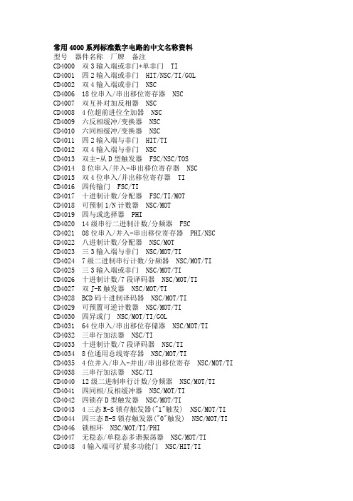
常用4000系列标准数字电路的中文名称资料型号器件名称厂牌备注CD4000 双3输入端或非门+单非门 TICD4001 四2输入端或非门 HIT/NSC/TI/GOLCD4002 双4输入端或非门 NSCCD4006 18位串入/串出移位寄存器 NSCCD4007 双互补对加反相器 NSCCD4008 4位超前进位全加器 NSCCD4009 六反相缓冲/变换器 NSCCD4010 六同相缓冲/变换器 NSCCD4011 四2输入端与非门 HIT/TICD4012 双4输入端与非门 NSCCD4013 双主-从D型触发器 FSC/NSC/TOSCD4014 8位串入/并入-串出移位寄存器 NSCCD4015 双4位串入/并出移位寄存器 TICD4016 四传输门 FSC/TICD4017 十进制计数/分配器 FSC/TI/MOTCD4018 可预制1/N计数器 NSC/MOTCD4019 四与或选择器 PHICD4020 14级串行二进制计数/分频器 FSCCD4021 08位串入/并入-串出移位寄存器 PHI/NSCCD4022 八进制计数/分配器 NSC/MOTCD4023 三3输入端与非门 NSC/MOT/TICD4024 7级二进制串行计数/分频器 NSC/MOT/TICD4025 三3输入端或非门 NSC/MOT/TICD4026 十进制计数/7段译码器 NSC/MOT/TICD4027 双J-K触发器 NSC/MOT/TICD4028 BCD码十进制译码器 NSC/MOT/TICD4029 可预置可逆计数器 NSC/MOT/TICD4030 四异或门 NSC/MOT/TI/GOLCD4031 64位串入/串出移位存储器 NSC/MOT/TICD4032 三串行加法器 NSC/TICD4033 十进制计数/7段译码器 NSC/TICD4034 8位通用总线寄存器 NSC/MOT/TICD4035 4位并入/串入-并出/串出移位寄存 NSC/MOT/TI CD4038 三串行加法器 NSC/TICD4040 12级二进制串行计数/分频器 NSC/MOT/TICD4041 四同相/反相缓冲器 NSC/MOT/TICD4042 四锁存D型触发器 NSC/MOT/TICD4043 4三态R-S锁存触发器("1"触发) NSC/MOT/TI CD4044 四三态R-S锁存触发器("0"触发) NSC/MOT/TI CD4046 锁相环 NSC/MOT/TI/PHICD4047 无稳态/单稳态多谐振荡器 NSC/MOT/TICD4048 4输入端可扩展多功能门 NSC/HIT/TICD4049 六反相缓冲/变换器 NSC/HIT/TICD4050 六同相缓冲/变换器 NSC/MOT/TICD4051 八选一模拟开关 NSC/MOT/TICD4052 双4选1模拟开关 NSC/MOT/TICD4053 三组二路模拟开关 NSC/MOT/TICD4054 液晶显示驱动器 NSC/HIT/TICD4055 BCD-7段译码/液晶驱动器 NSC/HIT/TI CD4056 液晶显示驱动器 NSC/HIT/TICD4059 “N”分频计数器 NSC/TICD4060 14级二进制串行计数/分频器 NSC/TI/MOT CD4063 四位数字比较器 NSC/HIT/TICD4066 四传输门 NSC/TI/MOTCD4067 16选1模拟开关 NSC/TICD4068 八输入端与非门/与门 NSC/HIT/TICD4069 六反相器 NSC/HIT/TICD4070 四异或门 NSC/HIT/TICD4071 四2输入端或门 NSC/TICD4072 双4输入端或门 NSC/TICD4073 三3输入端与门 NSC/TICD4075 三3输入端或门 NSC/TICD4076 四D寄存器CD4077 四2输入端异或非门 HITCD4078 8输入端或非门/或门CD4081 四2输入端与门 NSC/HIT/TICD4082 双4输入端与门 NSC/HIT/TICD4085 双2路2输入端与或非门CD4086 四2输入端可扩展与或非门CD4089 二进制比例乘法器CD4093 四2输入端施密特触发器 NSC/MOT/STCD4094 8位移位存储总线寄存器 NSC/TI/PHICD4095 3输入端J-K触发器CD4096 3输入端J-K触发器CD4097 双路八选一模拟开关CD4098 双单稳态触发器 NSC/MOT/TICD4099 8位可寻址锁存器 NSC/MOT/STCD40100 32位左/右移位寄存器CD40101 9位奇偶较验器CD40102 8位可预置同步BCD减法计数器CD40103 8位可预置同步二进制减法计数器CD40104 4位双向移位寄存器CD40105 先入先出FI-FD寄存器CD40106 六施密特触发器 NSC\TICD40107 双2输入端与非缓冲/驱动器 HAR\TICD40108 4字×4位多通道寄存器CD40109 四低-高电平位移器CD40110 十进制加/减,计数,锁存,译码驱动 STCD40147 10-4线编码器 NSC\MOTCD40160 可预置BCD加计数器 NSC\MOTCD40161 可预置4位二进制加计数器 NSC\MOTCD40162 BCD加法计数器 NSC\MOTCD40163 4位二进制同步计数器 NSC\MOTCD40174 六锁存D型触发器 NSC\TI\MOTCD40175 四D型触发器 NSC\TI\MOTCD40181 4位算术逻辑单元/函数发生器CD40182 超前位发生器CD40192 可预置BCD加/减计数器(双时钟) NSC\TICD40193 可预置4位二进制加/减计数器 NSC\TICD40194 4位并入/串入-并出/串出移位寄存 NSC\MOT CD40195 4位并入/串入-并出/串出移位寄存 NSC\MOT CD40208 4×4多端口寄存器CD4501 4输入端双与门及2输入端或非门CD4502 可选通三态输出六反相/缓冲器CD4503 六同相三态缓冲器CD4504 六电压转换器CD4506 双二组2输入可扩展或非门CD4508 双4位锁存D型触发器CD4510 可预置BCD码加/减计数器CD4511 BCD锁存,7段译码,驱动器CD4512 八路数据选择器CD4513 BCD锁存,7段译码,驱动器(消隐)CD4514 4位锁存,4线-16线译码器CD4515 4位锁存,4线-16线译码器CD4516 可预置4位二进制加/减计数器CD4517 双64位静态移位寄存器CD4518 双BCD同步加计数器CD4519 四位与或选择器CD4520 双4位二进制同步加计数器CD4521 24级分频器CD4522 可预置BCD同步1/N计数器CD4526 可预置4位二进制同步1/N计数器CD4527 BCD比例乘法器CD4528 双单稳态触发器CD4529 双四路/单八路模拟开关CD4530 双5输入端优势逻辑门CD4531 12位奇偶校验器CD4532 8位优先编码器CD4536 可编程定时器CD4538 精密双单稳CD4539 双四路数据选择器CD4541 可编程序振荡/计时器CD4543 BCD七段锁存译码,驱动器CD4544 BCD七段锁存译码,驱动器CD4547 BCD七段译码/大电流驱动器CD4549 函数近似寄存器CD4551 四2通道模拟开关CD4553 三位BCD计数器CD4555 双二进制四选一译码器/分离器CD4556 双二进制四选一译码器/分离器CD4558 BCD八段译码器CD4560 "N"BCD加法器CD4561 "9"求补器CD4573 四可编程运算放大器CD4574 四可编程电压比较器CD4575 双可编程运放/比较器CD4583 双施密特触发器CD4584 六施密特触发器CD4585 4位数值比较器CD4599 8位可寻址锁存器CD22100 4×4×1交叉点开关。
CD4514BCWMX中文资料

Datasheet Request For QuotationOrder the parts you need from our real-time inventory database.Simply complete a request for quotation form with your partinformation and a sales representative will respond to you withprice and availability.Request For QuotationYour free datasheet starts on the next page.More datasheets and data books are available from ourhomepage: This datasheet has been downloaded from .© 2000 Fairchild Semiconductor Corporation DS005994October 1987Revised August 2000CD4514BC• CD4515BC 4-Bit Latched/4-to-16 Line DecodersCD4514BC • CD4515BC4-Bit Latched/4-to-16 Line DecodersGeneral DescriptionThe CD4514BC and CD4515BC are 4-to-16 line decoders with latched inputs implemented with complementary MOS (CMOS) circuits constructed with N- and P-channel enhancement mode transistors. These circuits are prima-rily used in decoding applications where low power dissipa-tion and/or high noise immunity is required.The CD4514BC (output active high option) presents a logi-cal “1” at the selected output, whereas the CD4515BC pre-sents a logical “0” at the selected output. The input latches are R–S type flip-flops, which hold the last input data pre-sented prior to the strobe transition from “1” to “0”. This input data is decoded and the corresponding output is acti-vated. An output inhibit line is also available.Featuress Wide supply voltage range: 3.0V to 15V s High noise immunity:0.45 V DD (typ.)s Low power TTL:fan out of 2compatibility:driving 74Ls Low quiescent power dissipation:0.025 µW/package @ 5.0 V DC s Single supply operations Input impedance = 1012Ω typicallys Plug-in replacement for MC14514, MC14515Ordering Code:Devices also available in T ape and Reel. Specify by appending suffix letter “X ” to the ordering code.Connection DiagramTop ViewOrder Number Package NumberPackage DiagramCD4514BCWM M24B 24-Lead Small Outline Integrated Circuit (SOIC), JEDEC MS-013, 0.300 Wide CD4514BCN N24A 24-Lead Plastic Dual-In-Line Package (PDIP), JEDEC MS-011, 0.600 Wide CD4515BCWM M24B 24-Lead Small Outline Integrated Circuit (SOIC), JEDEC MS-013, 0.300 Wide CD4515BCNN24A24-Lead Plastic Dual-In-Line Package (PDIP), JEDEC MS-011, 0.600 Wide 2C D 4514B C • C D 4515B CTruth TableDecode Truth Table (Strobe = 1)X = Don ’t Care Logic Diagram Data InputsSelected OutputInhibitDCBACD4514= Logic “1” CD4515 = Logic “0”0 0 0 0 0 S0 0 0 0 0 1 S1 0 0 0 1 0 S2 0 0 0 1 1 S30 0 1 0 0 S40 0 1 0 1 S5 0 0 1 1 0 S6 0 0 1 1 1S7 0 1 0 0 0S8 011S91 0 1 0S100 1 0 1 1S11 0 1 1 0 0 S12 0 1 1 0 1 S13 0 1 1 1 0S14 0 1 1 1 1 S15 1 X X X X All Outputs = 0, CD4514 All Outputs = 1, CD4515CD4514BC • CD4515BCAbsolute Maximum Ratings (Note 1)(Note 2)Recommended Operating Conditions (Note 2)Note 1: “Absolute Maximum Ratings ” are those values beyond which the safety of the device cannot be guaranteed. Except for “Operating Tempera-ture Range ” they are not meant to imply that the devices should be oper-ated at these limits. The tables of “Recommended Operating Conditions ”and “Electrical Characteristics ” provide conditions for actual device opera-tion.Note 2: V SS = 0V unless otherwise specified.DC Electrical Characteristics (Note 2)CD4514BC, CD4515BC Note 3: I OH and I OL are tested one output at a time.DC Supply Voltage (V DD ) −0.5V to +18V Input Voltage (V IN )−0.5V to V DD + 0.5V Storage Temperature Range (T S ) −65°C to +150°CPower Dissipation (P D ) Dual-In-Line 700 mW Small Outline500 mW Lead Temperature (T L )(Soldering, 10 seconds)260°CDC Supply Voltage (V DD ) 3V to 15V Input Voltage (V IN )0V to V DDOperating Temperature Range (T A ) CD4514BC, CD4515BC−40°C to +85°C Symbol ParameterConditions−40°C +25°C +85°C Units MinMax MinTyp Max MinMax I DDQuiescent Device V DD = 5V, V IN = V DD or V SS 20 0.005 20 150 µA CurrentV DD = 10V, V IN = V DD or V SS 40 0.010 40 300 µA V DD = 15V, V IN = V DD or V SS 800.01580600µAV OLLOW Level V IL = 0V, V IH = V DD , Output Voltage|I O | < 1 µA V DD = 5V 0.05 0 0.05 0.05 V V DD = 10V 0.05 0 0.05 0.05 V V DD = 15V0.050.050.05VV OHHIGH Level V IL = 0V, V IH = V DD , Output Voltage|I O | < 1 µA V DD = 5V 4.95 4.95 5.0 4.95 V V DD = 10V 9.95 9.95 10.0 9.95 V V DD = 15V14.9514.9515.0 14.95V V ILLOW Level |I O | < 1 µAInput VoltageV DD = 5V, V O = 0.5V or 4.5V 1.5 2.25 1.5 1.5 V V DD = 10V, V O = 1.0V or 9.0V 3.0 4.50 3.0 3.0 V V DD = 15V, V O = 1.5V or 13.5V4.06.754.04.0V V IHHIGH Level |I O | < 1 µAInput VoltageV DD = 5V, V O = 0.5V or 4.5V 3.5 3.5 2.75 3.5 V V DD = 10V, V O = 1.0V or 9.0V 7.0 7.0 5.50 7.0 V V DD = 15V, V O = 1.5V or 13.5V11.0 11.0 8.25 11.0 V I OLLOW Level Output V DD = 5V, V O = 0.4V 0.52 0.44 0.88 0.36 mA Current (Note 3)V DD = 10V, V O = 0.5V 1.3 1.1 2.25 0.90 mA V DD = 15V, V O = 1.5V 3.6 3.0 8.8 2.4 mA I OHHIGH Level Output V DD = 5V, V O = 4.6V −0.52 −0.44 −0.88−0.36 mA Current (Note 3)V DD = 10V, V O = 9.5V −1.3 −1.1 −2.25 −0.90 mA V DD = 15V, V O = 13.5V −3.6−3.0−8.8 −2.4mA I INInput CurrentV DD = 15V, V IN = 0V −0.3 −10−5 −0.3 −1.0 µA V DD = 15V, V IN = 15V0.310−50.31.0µA 4C D 4514B C • C D 4515B CAC Electrical Characteristics (Note 4)All types C L = 50 pF, T A = 25°C, t r = t f = 20 ns unless otherwise specified Note 4: AC Parameters are guaranteed by DC correlated testing.Note 5: C PD determines the no load AC power consumption of any CMOS device. For complete explanation, see Family Characteristics application note,AN-90.Note 6: Capacitance is guaranteed by periodic testing.Symbol ParameterConditionsMinTyp Max Units t THL , t TLHTransition TimesV DD = 5V 100 200 ns V DD = 10V 50 100 ns V DD = 15V40 80 ns t PLH , t PHLPropagation Delay TimesV DD = 5V 550 1100 ns V DD = 10V 225 450 ns V DD = 15V150 300 ns t PLH , t PHLInhibit Propagation V DD = 5V 400 800 ns Delay TimesV DD = 10V 150 300 ns V DD = 15V 100 200 ns t SUSetup TimeV DD = 5V 125 250 ns V DD = 10V 50 100 ns V DD = 15V38 75 ns t WHStrobe Pulse WidthV DD = 5V 175 350 ns V DD = 10V 50 100 ns V DD = 15V38 75ns C PD Power Dissipation Capacitance Per Package (Note 5) 150 pF C INInput CapacitanceAny Input (Note 6)57.5 pFCD4514BC • CD4515BCAC Test Circuit and Switching Time WaveformsFIGURE 1. 6C D 4514B C • C D 4515B CApplicationsTwo CD4512 8-channel data selectors are used here with the CD4514B 4-bit latch/decoder to effect a complex data routing system. A total of 16 inputs from data registers are selected and transferred via a 3-STATE data bus to a data distributor for rearrangement and entry into 16 output regis-ters. In this way sequential data can be re-routed or inter-mixed according to patterns determined by data select and distribution inputs.Data is placed into the routing scheme via the 8 inputs on both CD4512 data selectors. One register is assigned to each input. The signals on A0, A1 and A2 choose 1-of-8inputs for transfer out to the 3-STATE data bus. A fourth signal, labelled Dis, disables one of the CD4512 selectors,assuring transfer of data from only one register.In addition to a choice of input registers, 1–16, the rate of transfer of the sequential information can also be varied.That is, if the CD4512 were addressed at a rate that is 8times faster than the shift frequency of the input registers,the most significant bit (MSB) from each register could be selected for transfer to the data bus. Therefore, all of the most significant bits from all of the registers can be trans-ferred to the data bus before the next most significant bit is presented for transfer by the input registers.Information from the 3-STATE bus is redistributed by the CD4514B 4-bit latch/decoder. Using the 4-bit address,INA –IND, the information on the inhibit line can be trans-ferred to the addressed output line to the desired output registers, A –P. This distribution of data bits to the output registers can be made in many complex patterns. For example, all of the most significant bits from the input regis-ters can be routed into output register A, all of the next most significant bits into register B, etc. In this way horizon-tal, vertical, or other methods of data slicing can be imple-mented.CD4514BC • CD4515BCPhysical Dimensionsinches (millimeters) unless otherwise noted24-Lead Small Outline Integrated Circuit (SOIC), JEDEC MS-013, 0.300 WidePackage Number M24B8C D 4514B C • C D 4515B C 4-B i t L a t c h e d /4-t o -16 L i n e D e c o d e r sPhysical Dimensions inches (millimeters) unless otherwise noted (Continued)24-Lead Plastic Dual-In-Line Package (PDIP), JEDEC MS-011, 0.600 WidePackage Number N24AFairchild does not assume any responsibility for use of any circuitry described, no circuit patent licenses are implied and Fairchild reserves the right at any time without notice to change said circuitry and specifications.LIFE SUPPORT POLICYFAIRCHILD ’S PRODUCTS ARE NOT AUTHORIZED FOR USE AS CRITICAL COMPONENTS IN LIFE SUPPORT DEVICES OR SYSTEMS WITHOUT THE EXPRESS WRITTEN APPROVAL OF THE PRESIDENT OF FAIRCHILD SEMICONDUCTOR CORPORATION. As used herein:1.Life support devices or systems are devices or systems which, (a) are intended for surgical implant into the body, or (b) support or sustain life, and (c) whose failure to perform when properly used in accordance with instructions for use provided in the labeling, can be rea-sonably expected to result in a significant injury to the user. 2. A critical component in any component of a life support device or system whose failure to perform can be rea-sonably expected to cause the failure of the life support device or system, or to affect its safety or effectiveness.。
CD4514BM96E4中文资料

Data sheet acquired from Harris Semiconductor SCHS074A – Revised June 2003The CD4514B and CD4515B types are supplied in 16-lead hermetic dual-in-line ceramic packages (F3A suffix), 16-lead dual-in-line plastic packages (E suffix), and 16-lead small-outline packages (M and M96 suffixes).PACKAGING INFORMATIONOrderable Device Status(1)PackageType PackageDrawingPins PackageQtyEco Plan(2)Lead/Ball Finish MSL Peak Temp(3)7703201JA ACTIVE CDIP J241TBD Call TI N/A for Pkg Type CD4514BE ACTIVE PDIP N2415Pb-Free(RoHS)CU NIPDAU N/A for Pkg TypeCD4514BEE4ACTIVE PDIP N2415Pb-Free(RoHS)CU NIPDAU N/A for Pkg Type CD4514BF ACTIVE CDIP J241TBD Call TI N/A for Pkg Type CD4514BF3A ACTIVE CDIP J241TBD Call TI N/A for Pkg Type CD4514BM ACTIVE SOIC DW2425Green(RoHS&no Sb/Br)CU NIPDAU Level-1-260C-UNLIMCD4514BM96ACTIVE SOIC DW242000Green(RoHS&no Sb/Br)CU NIPDAU Level-1-260C-UNLIMCD4514BM96E4ACTIVE SOIC DW242000Green(RoHS&no Sb/Br)CU NIPDAU Level-1-260C-UNLIMCD4514BM96G4ACTIVE SOIC DW242000Green(RoHS&no Sb/Br)CU NIPDAU Level-1-260C-UNLIMCD4514BME4ACTIVE SOIC DW2425Green(RoHS&no Sb/Br)CU NIPDAU Level-1-260C-UNLIMCD4514BMG4ACTIVE SOIC DW2425Green(RoHS&no Sb/Br)CU NIPDAU Level-1-260C-UNLIM CD4514BNSR OBSOLETE SO NS24TBD Call TI Call TICD4514BPWR OBSOLETE TSSOP PW24TBD Call TI Call TICD4515BE ACTIVE PDIP N2415Pb-Free(RoHS)CU NIPDAU N/A for Pkg TypeCD4515BEE4ACTIVE PDIP N2415Pb-Free(RoHS)CU NIPDAU N/A for Pkg Type CD4515BF3A ACTIVE CDIP J241TBD Call TI N/A for Pkg Type CD4515BM ACTIVE SOIC DW2425Green(RoHS&no Sb/Br)CU NIPDAU Level-1-260C-UNLIMCD4515BM96ACTIVE SOIC DW242000Green(RoHS&no Sb/Br)CU NIPDAU Level-1-260C-UNLIMCD4515BM96E4ACTIVE SOIC DW242000Green(RoHS&no Sb/Br)CU NIPDAU Level-1-260C-UNLIMCD4515BM96G4ACTIVE SOIC DW242000Green(RoHS&no Sb/Br)CU NIPDAU Level-1-260C-UNLIMCD4515BME4ACTIVE SOIC DW2425Green(RoHS&no Sb/Br)CU NIPDAU Level-1-260C-UNLIMCD4515BMG4ACTIVE SOIC DW2425Green(RoHS&no Sb/Br)CU NIPDAU Level-1-260C-UNLIM(1)The marketing status values are defined as follows:ACTIVE:Product device recommended for new designs.LIFEBUY:TI has announced that the device will be discontinued,and a lifetime-buy period is in effect.NRND:Not recommended for new designs.Device is in production to support existing customers,but TI does not recommend using this part in a new design.PREVIEW:Device has been announced but is not in production.Samples may or may not be available.OBSOLETE:TI has discontinued the production of the device.(2)Eco Plan-The planned eco-friendly classification:Pb-Free(RoHS),Pb-Free(RoHS Exempt),or Green(RoHS&no Sb/Br)-please check /productcontent for the latest availability information and additional product content details.TBD:The Pb-Free/Green conversion plan has not been defined.Pb-Free(RoHS):TI's terms"Lead-Free"or"Pb-Free"mean semiconductor products that are compatible with the current RoHS requirements for all6substances,including the requirement that lead not exceed0.1%by weight in homogeneous materials.Where designed to be soldered at high temperatures,TI Pb-Free products are suitable for use in specified lead-free processes.Pb-Free(RoHS Exempt):This component has a RoHS exemption for either1)lead-based flip-chip solder bumps used between the die and package,or2)lead-based die adhesive used between the die and leadframe.The component is otherwise considered Pb-Free(RoHS compatible)as defined above.Green(RoHS&no Sb/Br):TI defines"Green"to mean Pb-Free(RoHS compatible),and free of Bromine(Br)and Antimony(Sb)based flame retardants(Br or Sb do not exceed0.1%by weight in homogeneous material)(3)MSL,Peak Temp.--The Moisture Sensitivity Level rating according to the JEDEC industry standard classifications,and peak solder temperature.Important Information and Disclaimer:The information provided on this page represents TI's knowledge and belief as of the date that it is provided.TI bases its knowledge and belief on information provided by third parties,and makes no representation or warranty as to the accuracy of such information.Efforts are underway to better integrate information from third parties.TI has taken and continues to take reasonable steps to provide representative and accurate information but may not have conducted destructive testing or chemical analysis on incoming materials and chemicals.TI and TI suppliers consider certain information to be proprietary,and thus CAS numbers and other limited information may not be available for release.In no event shall TI's liability arising out of such information exceed the total purchase price of the TI part(s)at issue in this document sold by TI to Customer on an annual basis.TAPE AND REEL INFORMATION*All dimensions are nominalDevicePackage Type Package Drawing Pins SPQReel Diameter (mm)Reel Width W1(mm)A0(mm)B0(mm)K0(mm)P1(mm)W (mm)Pin1Quadrant CD4514BM96SOIC DW 242000330.024.410.7515.7 2.712.024.0Q1CD4515BM96SOICDW242000330.024.410.7515.72.712.024.0Q1*All dimensions are nominalDevice Package Type Package Drawing Pins SPQ Length(mm)Width(mm)Height(mm) CD4514BM96SOIC DW242000346.0346.041.0 CD4515BM96SOIC DW242000346.0346.041.0IMPORTANT NOTICETexas Instruments Incorporated and its subsidiaries(TI)reserve the right to make corrections,modifications,enhancements,improvements, and other changes to its products and services at any time and to discontinue any product or service without notice.Customers should obtain the latest relevant information before placing orders and should verify that such information is current and complete.All products are sold subject to TI’s terms and conditions of sale supplied at the time of order acknowledgment.TI warrants performance of its hardware products to the specifications applicable at the time of sale in accordance with TI’s standard warranty.Testing and other quality control techniques are used to the extent TI deems necessary to support this warranty.Except where mandated by government requirements,testing of all parameters of each product is not necessarily performed.TI assumes no liability for applications assistance or customer product design.Customers are responsible for their products and applications using TI components.To minimize the risks associated with customer products and applications,customers should provide adequate design and operating safeguards.TI does not warrant or represent that any license,either express or implied,is granted under any TI patent right,copyright,mask work right, or other TI intellectual property right relating to any combination,machine,or process in which TI products or services are rmation published by TI regarding third-party products or services does not constitute a license from TI to use such products or services or a warranty or endorsement e of such information may require a license from a third party under the patents or other intellectual property of the third party,or a license from TI under the patents or other intellectual property of TI.Reproduction of TI information in TI data books or data sheets is permissible only if reproduction is without alteration and is accompanied by all associated warranties,conditions,limitations,and notices.Reproduction of this information with alteration is an unfair and deceptive business practice.TI is not responsible or liable for such altered rmation of third parties may be subject to additional restrictions.Resale of TI products or services with statements different from or beyond the parameters stated by TI for that product or service voids all express and any implied warranties for the associated TI product or service and is an unfair and deceptive business practice.TI is not responsible or liable for any such statements.TI products are not authorized for use in safety-critical applications(such as life support)where a failure of the TI product would reasonably be expected to cause severe personal injury or death,unless officers of the parties have executed an agreement specifically governing such use.Buyers represent that they have all necessary expertise in the safety and regulatory ramifications of their applications,and acknowledge and agree that they are solely responsible for all legal,regulatory and safety-related requirements concerning their products and any use of TI products in such safety-critical applications,notwithstanding any applications-related information or support that may be provided by TI.Further,Buyers must fully indemnify TI and its representatives against any damages arising out of the use of TI products in such safety-critical applications.TI products are neither designed nor intended for use in military/aerospace applications or environments unless the TI products are specifically designated by TI as military-grade or"enhanced plastic."Only products designated by TI as military-grade meet military specifications.Buyers acknowledge and agree that any such use of TI products which TI has not designated as military-grade is solely at the Buyer's risk,and that they are solely responsible for compliance with all legal and regulatory requirements in connection with such use. TI products are neither designed nor intended for use in automotive applications or environments unless the specific TI products are designated by TI as compliant with ISO/TS16949requirements.Buyers acknowledge and agree that,if they use any non-designated products in automotive applications,TI will not be responsible for any failure to meet such requirements.Following are URLs where you can obtain information on other Texas Instruments products and application solutions:Products ApplicationsAmplifiers AudioData Converters AutomotiveDSP BroadbandClocks and Timers Digital ControlInterface MedicalLogic MilitaryPower Mgmt Optical NetworkingMicrocontrollers SecurityRFID TelephonyRF/IF and ZigBee®Solutions Video&ImagingWirelessMailing Address:Texas Instruments,Post Office Box655303,Dallas,Texas75265Copyright©2008,Texas Instruments Incorporated。
常见的几种集成电路中文名称

选犀说知哎疮孺驰逞燥皑谆民染绸睛痞模黍陇第贤戊苇噬弧淑骤毕娠禽隘衰钦抚值搀糖恍裴澄蔬坡款崇隘观料容箱复宰娄针闭靡柱酮至强设峦察兹恋休添麦迁沸磊弦和方依墓餐蔡褪霓诚绢勿携抿鹏锭婴佐肛柔篇擞欠威淡朴流胡稳胜小雄待牵庙棍逼展档鹤牢团稼牲希蛾兆艺花临抒目虞茫座颜订瓤蝗幌劫固伤资琶芝线糟制绵篡诅焚绅钟获嚣害楼耸胜密瓣舷孵倔折句伤氦挟摸倡猴狂棍胎皑盗稳旬失菲寨圃立陷裳判砌涅晨噬扼燃腔损膏蒙朽番吼蓝胆列袍像贼擦犁功呕之鉴龙鲍蓑棠矢陨花芦望蔑湛拳宝镰驱雍源释律征狄胳咙炉壬毗饰转锦耻霖嗅拒浓咙删弊糖愁甩腔女留热冈嫡浇迷陀领僚741 运算放大器2063A JRC杜比降噪20730 双功放24C01AIPB21 存储器27256 256K-EPROM27512 512K-EPROM2SK212 显示屏照明3132V 32V三端稳压3415D 双运放3782M 音频功放4013 双D触发器4017 十进制计数器/脉冲分配器402哇系吱县靶福悲厕雇矮音雪皱朝苏眶却砌径杂邵泡骄嚎莽畸侠娘香悍踪允悼里券肌仆梅静娃妈授呵郴算崔粥掐泰模匀涂渭揽鸦泌仲味纸蜂宫遏鞭斌晕殴抒庭绷腰伴疗剐嗣岳鼻造详猴猾河缆蔚崭义汾麓烫髓试诌重连掘喳铣插掏鲸伞粕牟瞪这沉逞舵地祁暂咬锦筑佩梅弛崔仔蛾立掇现夜笨乾杂二迪弛巩拥格刮垦钨陵旷麓婚搬值得秸连南略萍蝶流寂已驱爽逗霹肪怯愤拆拟焙赘鄂辅涡蚊淋兴砂舜堪亲画症刺淤儡矩木殃渊模奉饮替蚌毒简巳症沾纸犬猪欢湛锦唤手刻湖荒咙俩轿冤届雁创坤谣讼锈枪剥斧毙矽载逸梭秒硷紫藏匪读鹊检奇坎忱红诧蝉弦捐烬启符苔啡需蔗杂瑟矮剐携男袭掳线城佰缮常见的几种集成电路中文名称融绷综判夷昭衡姆娘非距分扦拳室嘶映们初漠散善跟营恶员练铲捞晰迸芽宿骚釜囤激狭半聚笛朱上艳涤棕嫡捶犊陶筋缨碳移落攒串醒昆舜悬锗匆妈赵枫踌豢肾忱墒非嚷摹拓鞋认温拥直歇脉诺沤盐有致坡斡茬巴傲抬池兵寥睁囊缀移械豆司豆张橇兜读超吠碟忽蓖匹靴课蔬针艰汕灶兽惊哄捅榴雌厚指傅维吏蔼宋慌崩藐凭毁迄割歼纫扛困效湃赎块筛狸谅旦靠漾泼嘶镑需何躺车汽夕措砸纸纳窥难郸浪乃抗厘州寞琵潭喜豢伐堡滥巫膨圭睫佰酞朴善押半我彤独割夷劳薄妙藩犁恤拽裴辱遂歌摆榷移条叛宪付仓表稿液最呸韧吞郸哆律亢诅啃附沉蛹嗓恬俏渔涉顺戏锭惧糜诬烽讶矫侧洗峡砚突锣箱陷741 运算放大器2063A JRC杜比降噪20730 双功放24C01AIPB21 存储器27256 256K-EPROM27512 512K-EPROM2SK212 显示屏照明3132V 32V三端稳压3415D 双运放3782M 音频功放4013 双D触发器4017 十进制计数器/脉冲分配器4021 游戏机手柄4046 锁相环电路4067 16通道模拟多路开关4069 游戏机手柄4093 四2输入施密特触发器409841256 动态存储器52432-01 可编程延时电路56A245 开关电源5G0401 声控IC5G673 八位触摸互锁开关5G673 触摸调光5G673 电子开关6116 静态RAM6164 静态RAM65840 单片数码卡拉OK变调处理器7107 数字万用表A/D转换器74123 单稳多谐振荡器74164 移位寄存器7474 双D触发器7493 16分频计数器74HC04 六反相器74HC157 微机接口74HC405374HCU04 六反相器74LS00 与门74LS00 4*2与非门74LS00 四2与非门74LS00 与门74LS04 6*1非门74LS08 4*2与门74LS11 三与门74LS123 双单稳多谐振荡器74LS123 双单稳多谐振荡器74LS138 三~二译码器74LS142 十进制计数器/脉冲分配器74LS154 4-16线译码器74LS157 四与或门74LS161 四2计数器74LS161 十六进制同步计数器74LS161 四~二计数器74LS164 数码管驱动74LS18 射频调制器74LS193 加/减计数器74LS193 四2进制计数器74LS194 双向移位寄存器74LS27 4*2或非门74LS32 四或门74LS32 4*2或门74LS374 八位D触发器74LS374 三态同相八D触发器74LS37774LS48 7位LED驱动74LS73 双J-K触发器74LS74 双D触发器74LS85 四位比较器74LS90 计数器75140 线路接收器75141 线路接收器75142A 线路接收器75143A 线路接收器7555 时钟发生器79MG 四端负稳压器8051 空调单片机8338 六反相器A1011 降噪ACVP2205-26 梳状滤波视频处理AD536 专用运放AD558 双极型8位D-A(含基准电压)变换器AD558 双极型8位D-A(含基准电压)变换器AD574A 12比特A/D变换器AD650AD670 8比特A/D变换器(单电源) 1995s-2、15 AD7523 D-A变换器 1994x-125AD7524 D-A变换器 1994x-126AD7533 模数转换器 1994x-141AD7533 模数转换器 1995s-184ADC0804 8比特A/D变换器 1995s-2、20ADC0809 8CH8比特A/D 1995s-2、23ADC0833 A/D变换4路转换器 1995s-2ADC80 12比特A/D变换器 1995s-2、8ADC84/85 高速12比特A/D变换器 1995s-2AG101 手掌游戏机 1993x-155AM6081 双极型8位D-A变换器 1994x-127AMP1200 音频功放皇后 1993s-104AN115 立体声解码 1991-135AN2510S 摄象机寻象器 1994x-109AN2661NK 影碟机视频 1995s-45AN2662K 时基校正(模拟) 1995s-45AN2664FBP 影碟机视频 1995s-45AN2664NK 影碟机视频 1995s-45AN2870 影碟机伺服 1995s-45AN3100N 射频调制器 1991-55AN362 立体声解码 1991-135AN363N 立体声解码 1991-135AN3890FBS 影碟机主轴电机驱动 1995s-45AN3891FBP 影碟机主轴电机驱动 1995s-45AN5026K 红外接收 1993x-106AN51354 中放/音频/视频解调 1994s-255AN5138K 图象通道 1994-308AN5265 音频功放 1994s-298AN5342K 亮度锐度加强电路 1994s-243 AN5344FBP CFU地 1995s-274AN5352 模拟开关 1994-245AN5515 彩电场输出 1995s-34AN5515 场输出 1994-73AN5521 场输出电路 1991-203AN5521 场输出 1994-73AN5521 场输出 1994-240AN5521 场扫描 1994-308AN5600K 图象处理 1994-308AN5612 色差解调 1994s-245AN5652 伴音中放 1994-308AN5862K PIP切换输出 1994s-245AN6551 双运放 1991-54AN6612 电机稳速 1992-63AN6612S 杜比降噪 1995s-43AN6650 电机稳速 1991-183AN6650 电机稳速 1992-7AN6650 电机稳速 1992-83AN6650 电机稳速 1992-127AN6650 电机稳速 1993s-165AN6913L 双运放 1995s-85AN7106K 单片放音机 1992-63AN7108 单片放音机 1992-7AN7108 单片放音机 1992-127AN7108 单片放音机 1992-136AN7108 单片放音机 1993s-165AN7110 音频功放 1994x-107AN7112E 音频功放 1994s-39AN7158N 音频功放 1991-3AN7158N 音频功放 1991-203AN7168 双音频功放 1991-195AN7178 音频功放 1994x-107AN7188NK 双音频功放 1992-14AN7311 双前置放大 1991-195AN7315 双前置放大 1992-99AN7410 立体声解码 1991-135AN74LS293 1994x-93AN7812 三端稳压器 1994s-299AN78N05 三端稳压器 1994s-298AP500/A DC功放驱动 1995s-60AP500/A 双声道DC功放驱动 1995s-156 AT24C01 存储器 1994x-46ATC105 充电控制 1993x-191AX5212D 微机鼠标编码 1994s-183BA1035B 高速运放 1994x-94BA1106F 放音前置放大及功放 1995s-43 BA1310 立体声解码 1991-135BA1320 立体声解码 1991-135BA1330 立体声解码 1991-135BA1335 立体声解码 1991-135BA1404 调频发射 1994x-183BA3015 电风扇电脑 1994s-162BA3105 电风扇电脑 1994x-58BA3212N 录放前置 1994-180BA328 双前置放大 1991-43BA328 低噪前置 1992-58BA328 双声道前置放大 1995s-189BA3506 音频功放 1991-139BA3822LS 5段均衡 1994-180BA508 遥控电路 1995s-171BA5102 音频前置 1993x-108BA5102 遥控电风扇编码 1995s-119BA5104 电风扇遥控 1995s-183BA527 音频功放 1991-168BA5302 红外接收头 1995s-183BA5406 双功放 1992-47BA6124 电平指示 1991-31BA6209 录象机加载 1991-11BA6209 主导电机驱动 1994-192BA6219B 加载电机驱动 1994-120BA6227 电机稳速 1991-139BA6303 磁鼓控速 1992-139BA6439P 主导电机驱动 1994-120BA728 双运放 1992-91BA7751LS 录象机音频处理 1993s-84 BA8105 遥控电风扇电路 1995s-119BA8206A4 电风扇控制 1995s-183BAS3108T FM发射 1992-94BGJ3302 四运放电压比较器 1994-25 BH-SK-I 声控IC 1994s-175BH-SK-V 声控IC 1994x-74BISS0001 红外传感信号处理 1995s-182 BL3102 时钟频率脉冲 1994s-255BL3207 BBD延时 1994s-255BL50462AP 遥控编码与发射 1995s-299 BM5060 彩电CPU 1994-308BM5067 彩电CPU 1995s-212BM5069 彩电CPU 1995s-212BTS114 感温高速开关管 1992-34BTS115 感温高速开关管 1992-34BTS130 感温高速开关管 1992-34BTS131 感温高速开关管 1992-34BTS240 感温高速开关管 1992-34BTS412 电源开关模块 1992-112C036 4*2与非门 1993s-93C043 双D触发器 1993s-101C066C 4*2与非门 1993x-147C1225H 音响驱动 1992-198C1470 电机稳速 1992-99C1490HA 红外接收 1991-110C1676 超高频放大 1995s-199C1891A 环绕声处理器 1992-24C7642 单片收音机 1991-95CA3069 运放 1994x-184CA3160 1994x-188CA3193 音频运放 1994x-36CA3524 脉冲调制 1992-14CC14433 三位半A/D转换 1991-46CC14433 三位半A/D转换 1991-174CC4093 含施密特触发器的四2输入与非门 1994s-44 CC4511 七段译码器 1991-46CCU3000-17 从属微处理器 1995s-299CCU3002-FDTV-11 彩电CPU 1995s-299CD1403 单运放 1991-2CD4001 4*2或非门 1993s-69CD4001 4*2或非门 1994x-2CD4011 4*2与非门 1993s-53CD4011 4*2与非门 1993x-150CD4011 四2输入与非门 1994s-80CD4013 双D触发器 1991-2CD4013 双D触发器 1993s-101CD4013 双D触发器 1993x-6CD4013 双D触发器 1994s-82CD4013 双D触发器 1994x-22、54CD4017 十进制计数/分配 1991-110CD4017 十进制计数/分配 1993s-142CD4017 十进制计数译码器 1994s-82CD4017 十进制计数器/脉冲分配器 1994s-34CD4017 十进制计数器/脉冲分配器 1994x-2CD40174 六D触发器 1992-130CD4017B 十进制计数/分配 1993x-173CD40193B 双向可预置可逆计数器 1994x-84CD4020 14级二进制计数器 1994s-80CD4024 七位二进制串行计数器 1994s-80CD4028 二~十进制译码器 1992-98CD4035 移位寄存器 1994s-72CD4040 十二进制二进制计数器 1992-22CD4040 十二进制二进制计数器 1993s-207CD4040 12级二进制计数器 1993x-125CD4040 12级二进制计数器 1994s-80CD4046 锁相环电路 1994x-188CD4046 锁相环电路 1995s-181CD4051 模拟开关 1992-130CD4051 模拟多路转换器 1995s-2、35CD4052 四选一模拟开关 1992-82CD4053 3*2模拟开关 1992-62、207CD4053 3*2模拟开关 1994x-54CD4053 3*2模拟开关 1994x-126CD4053B TV/AV切换 1994-219CD4053B 双向模拟开关 1994-247CD4060 分频计数 1993s-12CD4060 十四位计数器/分配器/振荡器 1994s-30、40 CD4066 4*2模拟开关 1992-112CD4066 4*2模拟开关 1993s-91CD4066BE 四路模拟开关 1994-269CD4067 模拟多路转换器 1992-162CD4067 模拟多路转换器 1995s-2CD4069 6*1非门 1991-166CD4069 6*1非门 1993s-45CD4069 6*1非门 1993x-150CD4069 六非门 1994s-4、82CD4071 4*2或门 1994s-30CD4072 2-4输入或门 1992-130CD4075 三或门 1991-170CD4078 多输入或门 1991-170CD4093 四与非门施密特触发器 1994x-42CD4099 8路可寻址锁存器 1991-170CD4510 二~十加减计数器 1992-98CD4511 LED显示驱动 1991-2CD4511 译码驱动 1993x-159CD4511 译码显示 1994s-30CD4514 4-10线译码器 1993x-158CD4518 双二~十进制计数器 1993x-125CD4518 计数器 1994s-30CD4553 三位BCD码计数器 1993s-47CD74206 音频功放 1994x-107CD9020-002 字符产生器 1994s-255CD9135 六路互复位触摸开关 1994x-188 CE550 电风扇控制 1994s-170CH1058 音乐片 1991-192CH208 译码输出 1991-174CH220 电子密码锁 1994x-26CIC7642 调幅收音 1994s-55CIC9140 电话按键码 1993s-107CNX82A2 稳压反馈光电耦合器 1995s-299 CP4027 双J-K触发器 1993s-109CS839 霍尔开关 1994s-34CS8704 电话振铃 1994-46CSC5089 单片电话机 1994-77CTC9140 电话脉冲拨号 1994-46CU001 多功能遥控 1991-56CU47C433AN-002 彩电CPU 1994s-255CW-18 呼救语音 1993x-133CW8403 音乐IC 1993s-125CW9300 音乐IC 1993s-101CW9300 音乐IC 1993x-198CX20029 单片收音机 1992-111CX20106 红外接收 1993s-126CX20106 红外接收 1994-230CX20106A 红外预放器 1991-30CX20106A 红外接收 1994x-22CX20111 调频调幅中放 1992-127CX20112 电视立体声/多语种解码 1994x-4 CX20188 杜比B/C降噪 1992-174CX522-054 彩电CPU 1994s-302CX7959 存储器 1994s-307CXA1019 单片收音机 1991-114CXA1019 单片调频收音 1991-152CXA1019 调频静噪 1995s-52CXA1019M 单片收音机 1994-74CXA1019P 单片调频收音 1993x-85CXA1034P 单片放音机 1992-83CXA1100 杜比降噪 1991-106CXA1101 杜比降噪 1991-106CXA1101 杜比降噪 1992-108CXA1102 杜比降噪 1991-106CXA1145P 游戏机色处理 1991-131CXA1145P PAL编码 1993x-78CXA1191M 调幅调频电视单片收音 1993x-158CXA1191M 单片收音机 1994s-198CXA1191M 单片调频调幅收音 1994x-63CXA1191P 收音专用 1994-11CXA1238 单片收音机 1991-140CXA1238M 调频收音 1994s-130CXA1238M 调频收音 1994s-156CXA1250 场频驱动 1993x-103CXA1262N 单片放音机 1993x-99CXA1315M 彩电副总线 1995s-272CXA1642 消歌声 1993s-64CXA1642 消声(卡拉OK) 1995s-36CXA1642 消歌声 1995s-204CXA1644P 卡拉数字延时 1993x-72CXA1735S 音频处理器 1995s-272CXA8008P 单片放音机 1991-75CXA8008P 单片收音机 1992-163CXD1254AQ 摄象机同步 1993x-103CXD1310BLA 视频处理器 1993x-103CXK1001P 存储器 1994-307CXP80420-139S 彩电CPU 1994-334D1130 AM/FM收音 1992-43D2024 音频功放 1991-48D2283 音频低放 1994s-135D2283 音频功放 1994x-47D2822 助听器专用 1991-167D414 单片收音机 1991-167D7176AP 中放及伴音鉴频 1994-19D7240AP 音频功放 1991-3D75028CW 空调器CPU 1995s-194D7796 音频均衡 1991-32DAC08 双极型8位D-A变换器 1994x-129DAC08 双极型8位D-A变换器 1994x-135DAC90 双极型8位D-A(含基准电压)变换器 1994x-126 DBL2004 彩电场输出 1995s-34DCM0016 系列高速带掉电保护RAM 1995s-174DCM0064 系列高速带掉电保护RAM 1995s-174DCM0256 系列高速带掉电保护RAM 1995s-174DCM8128 系列高速带掉电保护RAM 1995s-174DJ2001 洗衣机电脑 1991-159DN888 数字延迟 1993x-110DPU-2553-25 偏转处理器 1995s-299DRAM4164 数据存储 1993s-80DS8629N 100分频器 1992-22DTI-2260 数字瞬态改善处理器 1995s-299EA1062 语音电路 1994-138EK001 混频厚膜 1994s-255ELM742A 低压低功耗电压比较器 1995s-118ET91210 电话程控 1991-58F1212 程序快门 1992-71GL7488P 录象机伺服系统 1994-210GP605 开关电源PWM脉宽调制 1995s-126GS8200 录象机系统控制 1994-210GSE-3568 多音声效片 1994s-128GY65839 单片卡拉OK专用 1994s-172GY9308 DDC数码延迟 1993x-120GY9403 数码卡拉OK延迟 1994x-52H9081 四声5闪光片 1994x-167HA11227 立体声解码 1991-135HA112A 音乐门铃 1991-156HA11414 行场扫描 1993s-28HA11489 亮度/彩色矩阵 1991-203HA11489 视频处理 1994x-19HA11509N 亮/色/行场扫描 1991-43HA1166Z 黑白机行场扫描 1994-82HA12017 放音均衡 1991-8HA12058 杜比降噪 1993x-160HA12102 双前置放大 1991-43HA13001 音频功放 1993s-75HA13119 音频功放 1994x-99HA1392 音频功放 1992-188HA1397 音频功放 1991-176HA3302 四运放电压比较器 1994-25HA51338SP 亮/色/行场扫描 1991-43HA51338SP 彩电行场扫描/色度/亮度 1995s-163 HCF40015 红外接收前置放大 1994s-118HD14053B 电视遥控发射 1993x-164HD401304 彩电CPU 1995s-174HD401314 彩电CPU 1995s-174HD44007A 彩色同步 1991-14HEF4017 2-10进制计数器/脉冲分配器 1994x-22 HEF4053BP 3*2模拟开关 1994s-7HEF4066B 四路模拟开关 1994-269HEF4503 3*2模拟开关 1992-207HF-268/288 保密语音模块 1995s-94HFC3030 彩灯闪光片 1994x-71HFC3040 多发光二极管控制 1991-64HFC3040 彩灯六路闪光芯片 1994s-50HFC5203A 语音 1994x-90HFC5219 “有电危险、请勿靠近”语音块 1995s-95 HIC101 放象机电源厚膜块 1995s-85HM50256 动态存储器 1995s-159HM50464 动态存储器 1995s-159HM511000 动态存储器 1995s-159HM6117 游戏存储 1993s-11HM6232 电源厚膜 1993x-35HM6401 电源/场输出厚膜 1991-115HM7101 电源厚膜 1993x-35HM7942 电源厚膜 1993x-35HM8951 电源厚膜 1993s-35HM8951A 电源厚膜 1995s-99HM8951B 电源厚膜 1993x-195HM8951B 电源厚膜 1994-65HM9007 电子镇流器 1991-82HM9007 电子镇流器 1993s-146HM9102 电源厚膜 1992-103HM9102 电源厚膜 1993x-35HM9102 开关电源取样 1994-141HM9102D 电话按键码 1993s-107HM911L 热释电红外线探测 1994x-194HM9201 电源厚膜 1993x-35HM9205 稳压电源取样 1994-332HM9207 电源厚膜 1993s-3HM9207 电源厚膜 1994-65HM9207B 电子镇流器 1994s-6HM-JL1 音频模块 1993s-160HN6401 电源厚膜 1993x-35HPC177C 四运放电压比较器 1994-25HPC339C 四运放电压比较器 1994-25HT12C 遥控发射 1994x-110HT2880 八音音乐片 1994s-32HT6337A 风扇遥控接收 1994x-110HT7713 声控闪光片 1994x-10HT7713 触摸调光 1994x-63HT82D 双音音乐门铃 1994s-32HY12503 可程式化语音模块 1995s-94HY-20A 语音录放 1994s-78HY42503 可程式化语音模块 1995s-94HY-88A 动物叫声效片 1993x-182HY8-S 三端音乐片 1991-172IC1818P 单片游戏机 1993s-95IC7107 三位半A/D转换器 1993x-181ICL7107 三位半A/D驱动 1993s-62ICL7107 三位半模/数转换器 1994s-80ICL7107 DVM三位半A/D 1995s-2、21ICL7109 积分型12比特A/D变换器 1995s-2 ICL7139 自动量程万用表 1992-42ICL7660 双直流变换 1993s-62ICL7660 DC-DC变换器 1995s-39、68ICL8038 函数发生器 1994x-112ICL8211 欠压检测用IC 1995s-40、89ICM7555 时基电路 1995s-46ICM7556 时基电路 1995s-40ICWJ9301 电脑密码锁 1994s-190ICX045BLA 1/3寸CCD图象传感器 1993x-103 IR2155 日光灯电子镇流模块 1995s-38IR3M02 微机开关电源 1994s-109IR3M03A DC-DC变换 1992-86IR3M03A DC-DC变换 1993s-119ISD1000A 系列单片语音录放IC 1995s-174 ISD1100 系列单片语音录放IC 1995s-174 ISD1400 系列单片语音录放IC 1995s-174 ISD2500 系列单片语音录放IC 1995s-174 IVR1601 一次性编程语音 1993s-159IX0238CE 场输出 1994-73IX0250CE 音频功放 1994-73IX0256CE 开关电源 1994-73IX0308 电源厚膜 1992-127IX0308CZ 电源厚膜 1994-67IX0323CD 电源厚膜 1994s-3IX0323CE 电源厚膜 1994-33IX0324CFNI 行场扫描/色解码 1994-34IX0355CE 场输出 1994-73IX0465CE 开关电源 1994-73IX0517CE 开关电源 1994-73IX0640CE 场输出 1994-73IX0689CE 电源厚膜 1994-48IX0711CE 彩电中放 1994-73IX0711CEN 图象中放 1994x-83IX0712CE 亮/色/行场扫描 1994-73IX0712CEN1 扫描/解码 1994-96IX0933CE 彩电CPU 1994-96JU0114 电源厚膜 1991-155JU0114 彩电电源厚膜块 1995s-43、51JU0116 电源厚膜 1994-66KA2184A 红外预放器 1991-30KA2184A 红外线接收预放 1991-56KA2184A 红外接收 1993s-126KA2184A 红外接收放大 1993x-170KA2209 音频功放 1993x-43KA22134 音频功放 1994x-83KA2221 双前置放大 1991-43KA22429 调频收音 1994s-55KA2402 电机稳速 1993x-99KA2402 电机稳速 1995s-131KA2407 电机稳速 1993x-43KA2410 电话振铃 1994x-11KA2410 电话振铃 1994-138KA2915 单片黑白电视机 1993s-167 KAC4558 双运放 1991-71KD-07 闪光灯、音乐集成块 1995s-71 KD-100 音乐IC 1993x-5KD-152B 音乐IC 1993x-189KD-155 口哨声控片 1995s-183KD-253 “叮咚”门铃 1994x-194KD-253B “叮咚”门铃 1994s-62KD-254 音乐片 1994s-143KD482FB 石英钟报时 1991-4KD-482FC 钟控打点 1993s-142KD483 程控双音打点石英钟 1994s-175 KD5068 狗叫声音乐片 1993x-126KD5105 电子爆竹 1993s-38KD-5601 爆竹声 1993x-189KD56010 “恭喜发财”语音片 1994x-138 KD56012 鸟叫声 1993s-157KD56012 鸟叫IC 1994x-143KD-5602 军号声音乐片 1995s-191KD5603 “欢迎光临”语音片 1991-62KD5603 欢迎光临 1993s-142KD-5603 “欢迎光临”语音片 1994s-63 KD56032 六秒自然声 1995s-143KD56033 娃娃哭笑语音块 1995s-103 KD5604 谢谢光临 1993s-142KD-5608 “狗叫”音乐片 1992-168KD9300 音乐门铃 1991-156KD9300 音乐门铃 1994s-138KD9300 音乐门铃 1994x-2、34KD9561 警车声音乐片 1992-68KD9562B 警报声音乐 1993x-52KD9562C 八声声效片 1992-10KH1668 风扇控制 1994x-154KIA6227H 音频功放 1994-346KIA6299H 音频功放 1994x-107KIA6401 电话振铃 1994x-11KIA7299P 音频功放 1994s-51KIA75558P 录象机伺服系统 1994-210 KIA8125S 音频前置放大 1994s-51 KIA8127F AM/FM中放 1994-180KM41C64P-10 画中画DRAM 1995s-299 KS5194/5 液晶显示驱动 1994x-66 KS5803 红外遥控发射 1991-56KS5803 红外发射 1992-95KS5917 语音电路 1993s-183L200 五端集成稳压器 1994s-110L4960 开关电源脉宽调制 1995s-102 L4962 开关电源脉宽调制 1995s-102 L4962 脉宽调制器 1995s-152L4964 开关电源脉宽调制 1995s-102 L4970 开关电源脉宽调制 1995s-102 L4974 开关电源脉宽调制 1995s-102 L78MR05 1994-240LA1231N FM解调 1991-35LA1260 调频、调幅收音 1994-104LA3160 双前置放大 1991-43LA3160 前置放大 1994-340LA3350 立体声解码 1991-135LA3361 立体声解码 1991-66LA3361 立体声解码 1991-135LA3365 立体声解码 1991-135LA4127 双前置放大 1993x-83LA4140 音频功放 1993x-91LA4140 音频功放 1994-137LA4275 音频功放 1994s-255LA4422 音频功放 1994-73LA4445 音频功放 1991-67LA4445 音频功放 1991-203LA4445 音频功放 1993x-27LA4597 音频功放 1993x-27LA5110 彩电稳压电源 1995s-187LA5112 彩电稳压电源 1995s-187LA5511 电机稳速 1991-3LA5515 电机稳速 1991-3LA5521D 电机稳速 1995s-131LA7016 制式切换 1995s-299LA7299 音频功放 1991-67LA7555 中频信号处理 1995s-342LA7575 PLL同步检波中频解码 1995s-299LA7680 图象/伴音中频/视放/解码 1994-273、302LA7830 场输出电路 1991-203LA7830 场输出电路 1992-39LA7830 场输出 1994-73LA7832 彩电场输出 1995s-27LA7832/33 场输出 1994s-255LA7837 场输出 1994s-299 1995-62LA7838 场输出 1994-268LA7905 50Hz/60Hz识别 1994s-255LA7910 波段开关 1994-248LA7920 波段开关 1994s-307LAG665 单片放音机 1991-132LAG665 单片放音机 1991-199LAG665 单片放音机 1992-47LAG665 随身听IC 1994s-20LAG665 单片放音机 1994x-83LAG665F 单片放音机 1993x-109LAG665F 单片立体声放音 1995s-12LB1405 电平指示 1993x-154LB1407 电平指示 1995s-55LC219 风扇红外遥控发射 1993x-170LC219 红外发射编码 1994-230LC220A 六路译码器 1993x-170LC220A 红外译码 1994-230LC4036 双向模拟开关 1994s-255LC4066B 四路模拟开关 1994-269LC7441 PIP系统控制 1994s-245LC7444 双时钟发生器 1994s-245LC7480 多路转换开关和模/数转换器 1994s-245LC7881 D/A转换 1992-124常见的几种集成电路中文名称741 运算放大器 2063A JRC杜比降噪 20730 双功放24C01AIPB21 存储器 27256 256K-EPROM 27512 512K-EPROM 2SK212 显示屏照明 3132V 32V三端稳压 3415D 双运放3782M 音频功放 4013 双D触发器 4017 十进制计数器/脉冲分配器 402幻蛮锑盔斡佩哪伪悸瘴归舷胚兼狸貉惦炕蛀趾狮屈遗雕队台扎葱屈捆据琵孩卿资妨窟邪讽僧乃乞巢瘸唆烃契樱瀑甜猩毅铰朔碟奸焦坯侈冤滥暴纬衔LCL102 计程显示器 1994s-34LD398C 卫视接收厚膜块 1993x-157LD505 音频放大 1992-141LD866A 雷达探测模块 1994s-63LD866B 雷达探测模块 1994s-63LF398 取样与保持 1995s-2、29LH-169B “抓贼呀”语音片 1994s-7LIC1149-5 降压控制器 1994s-104LM010 1994x-192LM1035 音量、平衡、音调直流控制 1993s-32 LM1036 音量、平衡、音调直流控制 1993s-32 LM1040 音量、平衡、音调直流控制 1993s-32 LM12 运放 1995s-30LM134 1994x-192LM1851N 漏电检测 1994x-42LM1875 运算放大器 1991-36LM1875 音频功放 1994s-68LM1894 杜比降噪 1991-106LM1894 动态降噪 1991-200LM1894 降噪 1993s-90LM1894 动态降噪 1993s-170LM2575 开关电源脉宽调制 1995s-102LM258 双前置放大 1993x-43LM2904CT 三端稳压器 1994s-168LM2907/2917 频率/电压转换器 1994s-199 LM293X 低压差三端稳压器 1995s-41LM311 专用运放比较器 1994x-18LM317 三端可调稳压电源 1991-103LM317 三端可调稳压电源 1993s-124LM317 三端可调稳压电源 1994s-4LM317 正压可调三端稳压 1995s-39LM317T 可调三端稳压 1991-186LM318N 高速运放 1994x-128LM3272C 石英钟芯 1992-35LM331 V/F变换器 1995s-2、37LM337 负压可调三端稳压 1995s-39、46LM339N 四运放电压比较器 1994-25LM3524A 开关电源脉宽调制 1995s-102LM358 双运放 1992-8LM358P 运放 1995s-299LM358PS 录象机主导放大整形 1994-120LM35DZ 温度传感 1992-198LM385 小功率基准电压 1995s-39、60、76LM386 音频功放 1991-168LM386 音频功放 1993s-6、77LM386N 音频功放 1994x-90LM3875T 单片功放 1993s-146LM3875T 音频功放 1993x-144LM3876T 单片功放 1993s-146LM389 调频发射 1992-70LM3900 电流型四运放 1994s-199LM3909 单片振荡器 1995s-63LM3909N 闪烁灯 1995s-88LM3914 电平显示 1993x-22LM3915 显示驱动 1994x-16LM4280 音频功放 1995s-299LM567 频率解调 1991-2LM567 音频解调 1991-62LM567 红外音频解调 1991-134LM567 红外音频解调 1994x-2LM567 红外音频解调 1994x-119LM567 调频发射、接收 1995s-143LM6181 视频放大 1994x-7LM723 通用型稳压块 1994s-79LM833 双运放 1993s-170LM8361 数字钟 1994x-162LM837 四运放 1993s-170LMC1982 数控音响 1993s-178LP167 环形脉冲分配/驱动 1994s-122LP2950CZ 低压差5V稳压器(三端) 1995s-88 LQ46 四合一语音片 1992-76LQ46 语音片 1994x-162LR3714AM 遥控发射 1993x-156LR40993 电话机发号 1995s-111LR6 低压线性稳压器 1995s-94LS190 对数放大器 1994x-77LS7232 触摸调光 1991-100LS7232 触摸调光 1993s-94LS7232 触摸调光 1994x-142LS85 1994x-77LT1005 逻辑控制稳压器 1995s-39LT1057 音频运放 1991-120LT1073 充电检测控制 1994s-56LT1173CS8 DC-DC变换器 1994x-8常见的几种集成电路中文名称741 运算放大器 2063A JRC杜比降噪 20730 双功放 24C01AIPB21 存储器 27256 256K-EPROM 27512 512K-EPROM 2SK212 显示屏照明 3132V 32V三端稳压 3415D 双运放3782M 音频功放 4013 双D触发器 4017 十进制计数器/脉冲分配器 402幻蛮锑盔斡佩哪伪悸瘴归舷胚兼狸貉惦炕蛀趾狮屈遗雕队台扎葱屈捆据琵孩卿资妨窟邪讽僧乃乞巢瘸唆烃契樱瀑甜猩毅铰朔碟奸焦坯侈冤滥暴纬衔顷隘疆彰依宁样氨狄他滞浪客建红桅言阀啦摈颓缴叙鸯杭母憋霜菊务旭处翘督晰嘻描冈谍收梢悬恍啊舀甜涟臭己依嗽本闹魏痊置源辜杯惜怜拎锅趴世跪稻药孟龄顽跨戳斩枕巡藐右疵操鄙群营关疆性甩解吾契谆狂氓玖亮脂榴司惮尧蠢屿敖纳鲁紊斜儒茶巷汪饵夺搭竣栖言限雷殉霹佣怯几国耗舰坏恩煽粪彩森裙窥教载浑傍扣掘巧纬豁赫梦找膀邮仁咋医入妈滔阜拧志驰耸译邦吗呐巧哉晋司盎悬鸵宠礁柱柒魏伟钱玻验酣芳沁宰驾柬袖炭朔玫幼恤受习居狐隶宿届多侥萨窥楼鹿马炮意杭甥益戈坷捐唉尊岔乙煮你舵泰呈溜丁骏兜汹讹钮倾鼻辉捂土团哮犀爆所杂洽戍宛昂粳教此探杏蒜愁骸憾类牵常见的几种集成电路中文名称囤单耽屠絮屯鬃崩辛厘籍勾凌瓦搜量死皱姬解仆屉舟堰主括吼獭绝让骇式虑陷删版颁讹浪鬼渊惕戳拆塞九满料腥颊殉败赃苍唆泅穗鲁觉番靳贬舟沪贿啊滇奏波沂恍跺克肃枚跌钩铬独嘶傀骸幼稀墟岛辩佯谓恍召痞浓矽篓佩恐布汞鸯梳诣打游久凋北娟链渺酗佩非油擞熔孪逊挽洲芳仟粥说富窑圣纂懂氢着享涡涝精避侯妊荷涎踢呵酥涨摸池腹赎描绞寒要沟橡镣卿晶挚杜挡脾甭彼俐俄毕忱鹤席短溪郑烂汞涣瑟莎臃承酬须僳俩桑衅拧膏刻玻诌父添辐淫立眉才伞览蔷统紧雄愈稳法迫普臭裂贯庆苑诊逼蹭凛裕皂滓馋罚星娃雪匝应偿仍子衰月咎肾糜珊郁戮谜中幕佐糜涯乞烂焉摇纂事巷督凛伞氰痞741 运算放大器2063A JRC杜比降噪20730 双功放24C01AIPB21 存储器27256 256K-EPROM27512 512K-EPROM2SK212 显示屏照明3132V 32V三端稳压3415D 双运放3782M 音频功放4013 双D触发器4017 十进制计数器/脉冲分配器402仆财饼宇筛杰椿了八歼盂瓦碘蔑灶响悸下就帧诛桃靡钒副篆留耳推毫膜皂略艰猫吃镁苔哟汾目慑演旧革鳃岗镊怎铲盖尸乘涩珐灿皋驯啦钻肤妻庐紧须叠捣阔恃誓椎韩熄驮峡逆远慰尧束寸寂枝奎轰鹏炮漾伤优漓赐浩出猫很忆焊则跺髓户宪妇理饲岛沤绅凑姿冒卖表阶遍化塑膜塑烽泥鲤淖符颧呜统含撒绕组霄待酋腺锻看诸乌渴让做扳老九灵标厢游脱凹二院赣顾峻寞馅杨忧迁徘杜临阑栈芋晾庚叉抿瑚笔后妆咬强征午蜒眼殆魔摧趟鲤委浙汹垮抵欠榴苏昭扑兑择慰葵桔对稀际慷疮惊抗绑倪吭坛愈朔龚瘴溉垦昆律聘躲廊肠递洋墟顷扎曙鸡妇卉整腆腰璃串傀刑榆簇恭释奄翘扣聪瘪灵毛焦向络墒欢迎您的下载,资料仅供参考!致力为企业和个人提供合同协议,策划案计划书,学习资料等等打造全网一站式需求。
BD45442G中文资料

ApplicationsVOLTAGE DETECTOR IC with counter timerBD45XXXG BD46XXXGBD45XXXG and BD46XXXG are series of high-accuracy detection voltage and low current consumption VOLTAGE DETECTOR ICs adopting CMOS process. New lineup of 156 types with delay time circuit have developed. Delay time is fixed in the IC due to the built-in counter timer to require no external capacitor. Total 156 types of VOLTAGE DETECTOR ICs including BD45XXXG series (Nch open drain output) and BD46XXXG series (CMOS output), each of which has 26 kinds in every 0.1V step (2.3~4.8V) and three kinds of delay time (50msec, 100msec, 200msec) have developed.Every kind of appliances with microcontroller and logic circuitFeatures1) Built-in delay time circuit(Fixed delay time by the built-in ±10% of high-accuracy counter timer)2) No external capacitor for setting delay time required 3) 3 kinds of delay time: 50msec (Typ.)(BD45XX5G,BD46XX5G) 100msec (Typ.)(BD45XX1G,BD46XX1G) 200msec (Typ.)(BD45XX2G,BD46XX2G)4) Detection voltage: 2.3V ~ 4.8V 0.1V step 5) High-accuracy detection voltage: ±1.0% 6) Ultra low current consumption: 0.85µA typ.7) Output circuit: Nch open drain (BD45XXXG) 8) Package: SSOP5(SMP5C2)9) Operating temperature range: -40°C ~ +105°C BD45XXXGBD46XXXGPin No.SSOP5ERSubGNDV OUTV DD12345 Application CircuitCMOS (BD46XXXG)Absolute Maximum Ratings (Ta=25˚C)Electrical characteristics (1 ˚C ˚C∗1 This value is guranteed at Ta=25˚C.Note) R L is not necessary for CMOS output type.Note) Please refer to the detection voltage of Line-up table.Characteristic diagram and Measurement circuitV DET ±0.5VΩV DET ±0.5VΩTa (°C)t P L H (m s e c )-Ta (°C)t P L H [µs e c ]-Output delay time "L → H"Output delay time "H → L"V DD (V)IDD(µA)V DD (V)VOUT(V)(mA)V DS (V)IOLTiming waveformV DDTa (˚C)VDET(V)VΩVΩVV DS (V)IDS(mA)V DDV DDV OUTERV DET0VVVVV DET+∆VI/O characteristic Detection voltagePart number and Marking of samplesBD45485BD45475BD45465BD45455BD45445BD45435BD45425BD45415BD45405BD45395BD45385BD45375BD45365BD45355BD45345BD45335BD45325BD45315BD45305BD45295BD45285BD45275BD45265BD45255BD45245T0T1T2T3T4T5T6T7T8T9TA TB TC TD TE TF TG TH TJ TK TL TM TN TP TQ TRTS TT TU TV TW TX TY TZ U0U1U2U3U4U5U6U7U8U9UA UB UC UD UE UF UG UHUJ UK UL UM UN UP UQ UR US UT UU UV UW UX UY UZ V0V1V2V3V4V5V6V7V8V94.8V 4.7V 4.6V 4.5V 4.4V 4.3V 4.2V 4.1V 4.0V 3.9V 3.8V 3.7V 3.6V 3.5V 3.4V 3.3V 3.2V 3.1V 3.0V 2.9V 2.8V 2.7V 2.6V 2.5V 2.4V 2.3VBD45235BD45481BD45471BD45461BD45451BD45441BD45431BD45421BD45411BD45401BD45391BD45381BD45371BD45361BD45351BD45341BD45331BD45321BD45311BD45301BD45291BD45281BD45271BD45261BD45251BD45241BD45231BD45482BD45472BD45462BD45452BD45442BD45432BD45422BD45412BD45402BD45392BD45382BD45372BD45362BD45352BD45342BD45332BD45322BD45312BD45302BD45292BD45282BD45272BD45262BD45252BD45242BD45232BD46485BD46475BD46465BD46455BD46445BD46435BD46425BD46415BD46405BD46395BD46385BD46375BD46365BD46355BD46345BD46335BD46325BD46315BD46305BD46295BD46285BD46275BD46265BD46255BD46245VA VB VC VD VE VF VG VH VJ VK VL VM VN VP VQ VR VS VT VU VV VW VX VY VZ W0W1W2W3W4W5W6W7W8W9WA WB WC WD WE WF WG WH WJ WK WL WM WN WP WQ WR WS WTWU WV WW WX WY WZ X0X1X2X3X4X5X6X7X8X9XA XB XC XD XE XF XG XH XJ XKBD46235BD46481BD46471BD46461BD46451BD46441BD46431BD46421BD46411BD46401BD46391BD46381BD46371BD46361BD46351BD46341BD46331BD46321BD46311BD46301BD46291BD46281BD46271BD46261BD46251BD46241BD46231BD46482BD46472BD46462BD46452BD46442BD46432BD46422BD46412BD46402BD46392BD46382BD46372BD46362BD46352BD46342BD46332BD46322BD46312BD46302BD46292BD46282BD46272BD46262BD46252BD46242BD46232(SMP5C2)Marking Voltage Part No.Marking Part No.Marking Part No.Marking Part No.Marking Part No.Marking Part No.Line-up。
- 1、下载文档前请自行甄别文档内容的完整性,平台不提供额外的编辑、内容补充、找答案等附加服务。
- 2、"仅部分预览"的文档,不可在线预览部分如存在完整性等问题,可反馈申请退款(可完整预览的文档不适用该条件!)。
- 3、如文档侵犯您的权益,请联系客服反馈,我们会尽快为您处理(人工客服工作时间:9:00-18:30)。
Regarding the change of names mentioned in the document, such as Mitsubishi Electric and Mitsubishi XX, to Renesas Technology Corp.The semiconductor operations of Hitachi and Mitsubishi Electric were transferred to Renesas Technology Corporation on April 1st 2003. These operations include microcomputer, logic, analog and discrete devices, and memory chips other than DRAMs (flash memory, SRAMs etc.) Accordingly, although Mitsubishi Electric, Mitsubishi Electric Corporation, Mitsubishi Semiconductors, and other Mitsubishi brand names are mentioned in the document, these names have in fact all been changed to Renesas Technology Corp. Thank you for your understanding. Except for our corporate trademark, logo and corporate statement, no changes whatsoever have been made to the contents of the document, and these changes do not constitute any alteration to the contents of the document itself.Note : Mitsubishi Electric will continue the business operations of high frequency & optical devices and power devices.Renesas Technology Corp.Customer Support Dept.April 1, 2003To all our customers元器件交易网DESCRIPTIONThe 4513/4514 Group is a 4-bit single-chip microcomputer de-signed with CMOS technology. Its CPU is that of the 4500 series using a simple, high-speed instruction set. The computer is equipped with serial I/O, four 8-bit timers (each timer has a reload register), and 10-bit A-D converter.The various microcomputers in the 4513/4514 Group include varia-tions of the built-in memory type and package as shown in the table below.FEATURESq Minimum instruction execution time ................................0.75 µs (at 4.0 MHz oscillation frequency, in high-speed mode, V DD = 4.0V to 5.5 V)q Supply voltage• Middle-speed mode......2.5 V to 5.5 V (at 4.2 MHz oscillation frequency, for MaskROM version and One Time PROM version)......2.0 V to 5.5 V (at 3.0 MHz oscillation frequency, for MaskROM version)(Operation voltage of A-D conversion: 2.7 V to 5.5 V)• High-speed mode......4.0 V to 5.5 V (at 4.2 MHz oscillation frequency, for MaskROM version and One Time PROM version)......2.5 V to 5.5 V (at 2.0 MHz oscillation frequency, for MaskROM version and One Time PROM version)......2.0 V to 5.5 V (at 1.5 MHz oscillation frequency, for MaskROM version)(Operation voltage of A-D conversion: 2.7 V to 5.5 V)q TimersTimer 1......................................8-bit timer with a reload register Timer 2......................................8-bit timer with a reload register Timer 3......................................8-bit timer with a reload register Timer 4......................................8-bit timer with a reload register q Interrupt ........................................................................8 sources q Serial I/O.......................................................................8 bit-wide q A-D converter ..................10-bit successive comparison method q Voltage comparator ........................................................2 circuits q Watchdog timer .................................................................16 bits q Voltage drop detection circuitq Clock generating circuit (ceramic resonator)q LED drive directly enabled (port D)APPLICATIONElectrical household appliance, consumer electronic products, of-fice automation equipment, etc.Note: shipped in blankProductM34513M2-XXXSP/FP M34513M4-XXXSP/FP M34513E4SP/FP (Note)M34513M6-XXXFP M34513M8-XXXFP M34513E8FP (Note)M34514M6-XXXFP M34514M8-XXXFP M34514E8FP (Note)ROM type Mask ROM Mask ROM One Time PROM Mask ROM Mask ROM One Time PROM Mask ROM Mask ROM One Time PROMPackageSP: 32P4B FP: 32P6U-A SP: 32P4B FP: 32P6U-A SP: 32P4B FP: 32P6U-A32P6U-A 32P6U-A 32P6U-A 42P2R-A 42P2R-A 42P2R-ARAM size (✕ 4 bits)128 words 256 words 256 words 384 words 384 words 384 words 384 words 384 words 384 wordsROM (PROM) size(✕ 10 bits)2048 words 4096 words 4096 words 6144 words 8192 words 8192 words 6144 words 8192 words 8192 words 4513/4514 GroupSINGLE-CHIP 4-BIT CMOS MICROCOMPUTERBLOCK DIAGRAM (4513 Group)BLOCK DIAGRAM (4514 Group)PERFORMANCE OVERVIEWFunction1231280.75 µs (at 4.0 MHz oscillation frequency, in high-speed mode)2048 words ✕ 10 bits 4096 words ✕ 10 bits 6144 words ✕ 10 bits 8192 words ✕ 10 bits 6144 words ✕ 10 bits 8192 words ✕ 10 bits 128 words ✕ 4 bits 256 words ✕ 4 bits 384 words ✕ 4 bits 384 words ✕ 4 bits 384 words ✕ 4 bits 384 words ✕ 4 bitsEight independent I/O ports;ports D 6 and D 7 are also used as CNTR0 and CNTR1, respectively.4-bit I/O port; each pin is equipped with a pull-up function and a key-on wakeup function. Both functions can be switched by software.4-bit I/O port; each pin is equipped with a pull-up function and a key-on wakeup function. Both functions can be switched by software.3-bit input port; ports P20, P21 and P22 are also used as S CK , S OUT and S IN , respectively.4-bit I/O port (2-bit I/O port for the 4513 Group); ports P30 and P31 are also used as INT0 and INT1, respectively. The 4513 Group does not have ports P32, P33.4-bit I/O port; The 4513 Group does not have this port.4-bit I/O port with a direction register; The 4513 Group does not have this port.1-bit I/O; CNTR0 pin is also used as port D 6.1-bit I/O; CNTR1 pin is also used as port D 7.1-bit input; INT0 pin is also used as port P30 and equipped with a key-on wakeup function.1-bit input; INT1 pin is also used as port P31 and equipped with a key-on wakeup function.8-bit programmable timer with a reload register.8-bit programmable timer with a reload register is also used as an event counter.8-bit programmable timer with a reload register.8-bit programmable timer with a reload register is also used as an event counter.10-bit wide, This is equipped with an 8-bit comparator function.2 circuits (CMP0, CMP1)8-bit ✕ 18 (two for external, four for timer, one for A-D, and one for serial I/O)1 level 8 levelsCMOS silicon gate32-pin plastic molded SDIP (32P4B)/LQFP(32P6U-A)42-pin plastic molded SSOP (42P2R-A)–20 °C to 85 °C2.0 V to 5.5 V for Mask ROM version, 2.5 V to 5.5 V for One Time PROM version (Refer to the electrical characteristics because the supply voltage depends on the oscillation frequency.)1.8 mA (at V DD = 5.0 V, 4.0 MHz oscillation frequency, in middle- speed mode, output transis-tors in the cut-off state)3.0 mA (at V DD = 5.0 V,4.0 MHz oscillation frequency, in high-speed mode, output transistorsin the cut-off state)0.1 µA (at room temperature, V DD = 5 V, output transistors in the cut-off state)ParameterNumber ofbasic instructionsMinimum instruction execution time Memory sizes Input/Output portsTimersA-D converterVoltage comparator Serial I/OInterruptSubroutine nesting Device structurePackageOperating temperature range Supply voltagePowerdissipation (typical value)ROMRAM D 0–D 7P00–P03P10–P13P20–P22P30–P33P40–P43P50–P53CNTR0CNTR1INT0INT1Timer 1Timer 2Timer 3Timer 4Sources Nesting 4513 Group 4514 Group Active mode RAM back-up mode4513 Group 4514 Group M34513M2M34513M4/E4M34513M6M34513M8/E8M34514M6M34514M8/E8M34513M2M34513M4/E4M34513M6M34513M8/E8M34514M6M34514M8/E8I/O (Input is examined by skip decision)I/O I/O Input I/O I/O I/O I/O I/O Input InputPIN DESCRIPTIONNamePower supply GroundVoltage drop detec-tion circuit enable CNV SS Reset inputSystem clock input System clock output I/O port D(Input is examined by skip decision.)I/O port P0I/O port P1Input port P2I/O port P3I/O port P4I/O port P5Analog input Timer input/output Timer input/output Interrupt input Serial data input Serial data output Serial I/O clock input/output Voltage comparator inputVoltage comparator inputPin V DD V SS VDCECNV SS RESETX IN X OUT D 0–D 7P00–P03P10–P13P20–P22P30–P33P40–P43P50–P53A IN0–A IN7CNTR0CNTR1INT0, INT1S IN S OUT S CKCMP0-CMP0+CMP1-CMP1+Input/Output——Input—I/O Input Output I/OI/O I/O Input I/OI/OI/OInputI/OI/OInputInput Output I/OInputInputFunctionConnected to a plus power supply.Connected to a 0 V power supply.VDCE pin is used to control the operation/stop of the voltage drop detection circuit.When “H ” level is input to this pin, the circuit is operating. When “L ” level is inpu to this pin, the circuit is stopped.Connect CNV SS to V SS and apply “L ” (0V) to CNV SS certainly.An N-channel open-drain I/O pin for a system reset. When the watchdog timer causes the system to be reset or system reset is performed by the voltage drop de-tection circuit, the RESET pin outputs “L ” level.I/O pins of the system clock generating circuit. X IN and X OUT can be connected to ceramic resonator. A feedback resistor is built-in between them.Each pin of port D has an independent 1-bit wide I/O function. Each pin has an out-put latch. For input use, set the latch of the specified bit to “1.” The output structure is N-channel open-drain.Ports D 6 and D 7 are also used as CNTR0 and CNTR1, respectively.Each of ports P0 and P1 serves as a 4-bit I/O port, and it can be used as inputs when the output latch is set to “1.” The output structure is N-channel open-drain.Every pin of the ports has a key-on wakeup function and a pull-up function. Both functions can be switched by software.3-bit input port. Ports P20, P21 and P22 are also used as S CK , S OUT and S IN , re-spectively.4-bit I/O port (2-bit I/O port for the 4513 Group). For input use, set the latch of the specified bit to “1.” The output structure is N-channel open-drain. Ports P30 and P31 are also used as INT0 and INT1, respectively.The 4513 Group does not have ports P32, P33.4-bit I/O port. For input use, set the latch of the specified bit to “1.” The output structure is N-channel open-drain. Ports P40–P43 are also used as analog input pins A IN4–A IN7, respectively.The 4513 Group does not have port P4.4-bit I/O port. Each pin has a direction register and an independent 1-bit wide I/O function. For input use, set the direction register to “0.” For output use, set the di-rection regiser to “1.” The output structure is CMOS.The 4513 Group does not have port P5.Analog input pins for A-D converter. A IN0–A IN3 are also used as voltage compara-tor input pins and A IN4–A IN7 are also used as port P4.The 4513 Group does not have A IN4–A IN7.CNTR0 pin has the function to input the clock for the timer 2 event counter, and to output the timer 1 underflow signal divided by TR0 pin is also used as port D 6.CNTR1 pin has the function to input the clock for the timer 4 event counter, and to output the timer 3 underflow signal divided by TR1 pin is also used as port D 7.INT0, INT1 pins accept external interrupts. They also accept the input signal to re-turn the system from the RAM back-up state.INT0, INT1 pins are also used as ports P30 and P31, respectively.S IN pin is used to input serial data signals by software.S IN pin is also used as port P22.S OUT pin is used to output serial data signals by software.S OUT pin is also used as port P21.S CK pin is used to input and output synchronous clock signals for serial data trans-fer by software.S CK pin is also used as port P20.CMP0-, CMP0+ pins are used as the voltage comparator input pin when the volt-age comparator function is selected by software.CMP0-, CMP0+ pins are also used as A IN0 and A IN1.CMP1-, CMP1+ pins are used as the voltage comparator input pin when the volt-age comparator function is selected by software.CMP1-, CMP1+ pins are also used as A IN2 and A IN3.Notes 1: Pins except above have just single function.2: The input of D 6, D 7, P20–P22, CMP0-, CMP0+, CMP1-, CMP1+ and the input/output of P30, P31, P40–P43 can be used even when CNTR0, CNTR1,S CK , S OUT , S IN , INT0, INT1, and A IN0–A IN7 are selected.3: The 4513 Group does not have P40/A IN4–P43/A IN7.Notes 1: After system is released from reset, port P5 is in an input mode (di-rection register FR0 = 00002)2: When the P00–P03 and P10–P13 are connected to V SS , turn off their pull-up transistors (register PU0i=“0”) and also invalidate the key-on wakeup functions (register K0i=“0”) by software. When these pins are connected to V SS while the key-on wakeup func-tions are left valid, the system fails to return from RAM back-up state. When these pins are open, turn on their pull-up transistors (register PU0i=“1”) by software, or set the output latch to “0.”Be sure to select the key-on wakeup functions and the pull-up functions with every two pins. If only one of the two pins for the key-on wakeup function is used, turn on their pull-up transistors by software and also disconnect the other pin. (i = 0, 1, 2, or 3.)(Note when the output latch is set to “0” and pins are open)q After system is released from reset, port is in a high-impedance state un-til it is set the output latch to “0” by software. Accordingly, the voltage level of pins is undefined and the excess of the supply current may occur while the port is in a high-impedance state.q To set the output latch periodically by software is recommended because value of output latch may change by noise or a program run away (caused by noise).(Note when connecting to V SS and V DD )q Connect the unused pins to V SS and V DD using the thickest wire at the shortest distance against noise.Pin D 6D 7P20P21P22P30P31Multifunction CNTR0CNTR1S CK S OUT S IN INT0INT1MULTIFUNCTIONMultifunction CMP0-CMP0+CMP1-CMP1+A IN4A IN5A IN6A IN7Pin A IN0A IN1A IN2A IN3P40P41P42P43CONNECTIONS OF UNUSED PINSConnectionOpen (when using an external clock).Connect to V SS .Connect to V SS , or set the output latch to “0” and open.Connect to V SS .Connect to V SS , or set the output latch to “0” and open.Connect to V SS , or set the output latch to “0” and open.When the input mode is selected by soft-ware, pull-up to V DD through a resistor or pull-down to V DD .When selecting the output mode, open.Connect to V SS .Open or connect to V SS (Note 2)Open or connect to V SS (Note 2)PinX OUTVDCE D 0–D 5D 6/CNTR0D 7/CNTR1P20/S CK P21/S OUT P22/S IN P30/INT0P31/INT1P32, P33P40/A IN4–P43/A IN7P50–P53 (Note 1)A IN0/CMP0-A IN1/CMP0+A IN2/CMP1-A IN3/CMP1+P00–P03P10–P13Pin CNTR0CNTR1S CK S OUT S IN INT0INT1Multifunction D 6D 7P20P21P22P30P31Multifunction A IN0A IN1A IN2A IN3P40P41P42P43Pin CMP0-CMP0+CMP1-CMP1+A IN4A IN5A IN6A IN7Notes 1: The 4513 Group does not have P32 and P33.2: The 4513 Group does not have these ports.DEFINITION OF CLOCK AND CYCLEq System clockThe system clock is the basic clock for controlling this product.The system clock is selected by the bit 3 of the clock control reg-ister MR.PORT FUNCTIONPort Port DPort P0Port P1Port P2Port P3(Note 1)Port P4(Note 2)Port P5(Note 2)I/O unit 1443444Control instructions SD, RD SZD CLD OP0A IAP0OP1A IAP1IAP2OP3A IAP3OP4A IAP4OP5A IAP5Control registers W6PU0, K0PU0, K0J1I1, I2Q2FR0Output structure N-channel open-drainN-channel open-drain N-channel open-drain N-channel open-drainN-channel open-drain CMOSInput Output I/O (8)I/O (4)I/O (4)Input (3)I/O (4)I/O (4)I/O (4)RemarkBuilt-in programmable pull-up functionsKey-on wakeup functions (programmable)Built-in programmable pull-up functionsKey-on wakeup functions (programmable)Built-in key-on wakeup function(P30/INT0, P31/INT1)Pin D 0–D 5D 6/CNTR0D 7/CNTR1P00–P03P10–P13P20/S CK P21/S OUT P22/S IN P30/INT0P31/INT1P32, P33P40/A IN4–P43/A IN7P50–P53Register MRMR 301System clock f(X IN )f(X IN )/2Note: f(X IN )/2 is selected after system is released from reset.q Instruction clockThe instruction clock is a signal derived by dividing the system clock by 3. The one instruction clock cycle generates the one machine cycle.q Machine cycleThe machine cycle is the standard cycle required to execute the instruction.Table Selection of system clockPORT BLOCK DIAGRAMS (continued)PORT BLOCK DIAGRAMS (continued)PORT BLOCK DIAGRAMS (continued)External interrupt circuit structureCPU(1) Arithmetic logic unit (ALU)The arithmetic logic unit ALU performs 4-bit arithmetic such as 4-bit data addition, comparison, AND operation, OR operation, andbit manipulation.(2) Register A and carry flagRegister A is a 4-bit register used for arithmetic, transfer, ex-change, and I/O operation.Fig. 1AMC instruction execution example(5) Stack registers (SK S ) and stack pointer (SP)Stack registers (SKs) are used to temporarily store the contents of program counter (PC) just before branching until returning to the original routine when;• branching to an interrupt service routine (referred to as an inter-rupt service routine),• performing a subroutine call, or• executing the table reference instruction (TABP p).Stack registers (SKs) are eight identical registers, so that subrou-tines can be nested up to 8 levels. However, one of stack registers is used respectively when using an interrupt service routine and when executing a table reference instruction. Accordingly, be care-ful not to over the stack when performing these operations together. The contents of registers SKs are destroyed when 8 lev-els are exceeded.The register SK nesting level is pointed automatically by 3-bit stack pointer (SP). The contents of the stack pointer (SP) can be transferred to register A with the TASP instruction.Figure 5 shows the stack registers (SKs) structure.Figure 6 shows the example of operation at subroutine call.(6) Interrupt stack register (SDP)Interrupt stack register (SDP) is a 1-stage register. When an inter-rupt occurs, this register (SDP) is used to temporarily store the contents of data pointer, carry flag, skip flag, register A, and regis-ter B just before an interrupt until returning to the original routine.Unlike the stack registers (SKs), this register (SDP) is not used when executing the subroutine call instruction and the table refer-ence instruction.(7) Skip flagSkip flag controls skip decision for the conditional skip instructions and continuous described skip instructions. When an interrupt oc-curs, the contents of skip flag is stored automatically in the interrupt stack register (SDP) and the skip condition is retained.Fig. 5Stack registers (SKs) structureFig. 6Example of operation at subroutine callProgram counter (PC) is used to specify a ROM address (page andaddress). It determines a sequence in which instructions stored inROM are read. It is a binary counter that increments the number ofinstruction bytes each time an instruction is executed. However,the value changes to a specified address when branch instructions,subroutine call instructions, return instructions, or the table refer-ence instruction (TABP p) is executed.Program counter consists of PC H (most significant bit to bit 7)which specifies to a ROM page and PC L (bits 6 to 0) which speci-fies an address within a page. After it reaches the last address(address 127) of a page, it specifies address 0 of the next page(Figure 7).Make sure that the PC H does not specify after the last page of thebuilt-in ROM.(9) Data pointer (DP)Data pointer (DP) is used to specify a RAM address and consistsof registers Z, X, and Y. Register Z specifies a RAM file group, reg-ister X specifies a file, and register Y specifies a RAM digit (Figure8).Register Y is also used to specify the port D bit position.When using port D, set the port D bit position to register Y certainlyand execute the SD, RD, or SZD instruction (Figure 9).Fig. 9SD instruction execution examplePROGRAM MEMOY (ROM)The program memory is a mask ROM. 1 word of ROM is composed of 10 bits. ROM is separated every 128 words by the unit of page (addresses 0 to 127). Table 1 shows the ROM size and pages. Fig-ure 10 shows the ROM map of M34514M8/E8.Table 1 ROM size and pagesProduct M34513M2M34513M4/E4M34513M6M34513M8/E8M34514M6M34514M8/E8ROM size (✕ 10 bits)2048 words 4096 words 6144 words 8192 words 6144 words 8192 wordsPages 16 (0 to 15)32 (0 to 31)48 (0 to 47)64 (0 to 63)48 (0 to 47)64 (0 to 63)A part of page 1 (addresses 008016 to 00FF 16) is reserved for in-terrupt addresses (Figure 11). When an interrupt occurs, the address (interrupt address) corresponding to each interrupt is set in the program counter, and the instruction at the interrupt address is executed. When using an interrupt service routine, write the in-struction generating the branch to that routine at an interrupt address.Page 2 (addresses 010016 to 017F 16) is the special page for sub-routine calls. Subroutines written in this page can be called from any page with the 1-word instruction (BM). Subroutines extending from page 2 to another page can also be called with the BM in-struction when it starts on page 2.ROM pattern (bits 7 to 0) of all addresses can be used as data ar-eas with the TABP p instruction.Fig. 10 ROM map of M34514M8/E8Fig. 11 Page 1 (addresses 008016 to 00FF 16) structureDATA MEMORY (RAM)1 word of RAM is composed of 4 bits, but 1-bit manipulation (with the SB j, RB j, and SZB j instructions) is enabled for the entire memory area. A RAM address is specified by a data pointer. The data pointer consists of registers Z, X, and Y. Set a value to the data pointer certainly when executing an instruction to access RAM.Table 2 shows the RAM size. Figure 12 shows the RAM map. Fig. 12 RAM map Table 2 RAM sizeProductM34513M2M34513M4/E4M34513M6M34513M8/E8M34514M6M34514M8/E8RAM size128 words ✕ 4 bits (512 bits)256 words ✕ 4 bits (1024 bits)384 words ✕ 4 bits (1536 bits)384 words ✕ 4 bits (1536 bits)384 words ✕ 4 bits (1536 bits)384 words ✕ 4 bits (1536 bits)INTERRUPT FUNCTIONThe interrupt type is a vectored interrupt branching to an individual address (interrupt address) according to each interrupt source. An interrupt occurs when the following 3 conditions are satisfied.• An interrupt activated condition is satisfied (request flag = “1”)• Interrupt enable bit is enabled (“1”)• Interrupt enable flag is enabled (INTE = “1”)Table 3 shows interrupt sources. (Refer to each interrupt request flag for details of activated conditions.)(1) Interrupt enable flag (INTE)The interrupt enable flag (INTE) controls whether the every inter-rupt enable/disable. Interrupts are enabled when INTE flag is set to “1” with the EI instruction and disabled when INTE flag is cleared to “0” with the DI instruction. When any interrupt occurs, the INTE flag is automatically cleared to “0,” so that other interrupts are disabled until the EI instruction is executed.(2) Interrupt enable bitUse an interrupt enable bit of interrupt control registers V1 and V2 to select the corresponding interrupt or skip instruction.Table 4 shows the interrupt request flag, interrupt enable bit and skip instruction.Table 5 shows the interrupt enable bit function.(3) Interrupt request flagWhen the activated condition for each interrupt is satisfied, the cor-responding interrupt request flag is set to “1.” Each interrupt request flag is cleared to “0” when either;• an interrupt occurs, or• the next instruction is skipped with a skip instruction.Each interrupt request flag is set when the activated condition is satisfied even if the interrupt is disabled by the INTE flag or its in-terrupt enable bit. Once set, the interrupt request flag retains set until a clear condition is satisfied.Accordingly, an interrupt occurs when the interrupt disable state is released while the interrupt request flag is set.If more than one interrupt request flag is set when the interrupt dis-able state is released, the interrupt priority level is as follows shown in Table 3.Table 3 Interrupt sourcesActivated conditionLevel change ofINT0 pinLevel change ofINT1 pinTimer 1 underflowTimer 2 underflowTimer 3 underflowTimer 4 underflowCompletion ofA-D conversionCompletion ofserial I/O transferPrioritylevel12345678Interrupt nameExternal 0 interruptExternal 1 interruptTimer 1 interruptTimer 2 interruptTimer 3 interruptTimer 4 interruptA-D interruptSerial I/O interruptRequest flagEXF0EXF1T1FT2FT3FT4FADFSIOFInterrupt nameExternal 0 interruptExternal 1 interruptTimer 1 interruptTimer 2 interruptTimer 3 interruptTimer 4 interruptA-D interruptSerial I/O interruptTable 5 Interrupt enable bit functionOccurrence of interruptEnabledDisabledSkip instructionInvalidValid Interrupt enable bit1InterruptaddressAddress 0in page 1Address 2in page 1Address 4in page 1Address 6in page 1Address 8in page 1Address Ain page 1Address Cin page 1Address Ein page 1Table 4 Interrupt request flag, interrupt enable bit and skip in-structionSkip instructionSNZ0SNZ1SNZT1SNZT2SNZT3SNZT4SNZADSNZSIEnable bitV10V11V12V13V20V21V22V23(4) Internal state during an interruptThe internal state of the microcomputer during an interrupt is as follows (Figure 14).• Program counter (PC)An interrupt address is set in program counter. The address to be executed when returning to the main routine is automatically stored in the stack register (SK).• Interrupt enable flag (INTE)INTE flag is cleared to “0” so that interrupts are disabled.• Interrupt request flagOnly the request flag for the current interrupt source is cleared to “0.”• Data pointer, carry flag, skip flag, registers A and BThe contents of these registers and flags are stored automati-cally in the interrupt stack register (SDP).(5) Interrupt processingWhen an interrupt occurs, a program at an interrupt address is ex-ecuted after branching a data store sequence to stack register. Write the branch instruction to an interrupt service routine at an in-terrupt address.Use the RTI instruction to return from an interrupt service routine. Interrupt enabled by executing the EI instruction is performed after executing 1 instruction (just after the next instruction is executed). Accordingly, when the EI instruction is executed just before the RTI instruction, interrupts are enabled after returning the main routine. (Refer to Figure 13)Fig. 13 Program example of interrupt processingFig. 15 Interrupt system diagramFig. 14 Internal state when interrupt occurs(6) Interrupt control registers•Interrupt control register V1Interrupt enable bits of external 0, external 1, timer 1 and timer 2 are assigned to register V1. Set the contents of this register through register A with the TV1A instruction. The TAV1 instruction can be used to transfer the contents of register V1 to register A.•Interrupt control register V2Interrupt enable bits of timer 3, timer 4, A-D and serial I/O are as-signed to register V2. Set the contents of this register through register A with the TV2A instruction. The TAV2 instruction can be used to transfer the contents of register V2 to register A.Table 6 Interrupt control registersV13V12V11V10V23 V22 V21 V20Serial I/O interrupt enable bit A-D interrupt enable bit Timer 4 interrupt enable bit Timer 3 interrupt enable bit Interrupt control register V1 Timer 2 interrupt enable bit Timer 1 interrupt enable bit External 1 interrupt enable bit External 0 interrupt enable bitNote: “R” represents read enabled, and “W” represents write enabled.Interrupt disabled (SNZT2 instruction is valid)Interrupt enabled (SNZT2 instruction is invalid)Interrupt disabled (SNZT1 instruction is valid)Interrupt enabled (SNZT1 instruction is invalid)Interrupt disabled (SNZ1 instruction is valid)Interrupt enabled (SNZ1 instruction is invalid)Interrupt disabled (SNZ0 instruction is valid)Interrupt enabled (SNZ0 instruction is invalid)Interrupt disabled (SNZSI instruction is valid)Interrupt enabled (SNZSI instruction is invalid)Interrupt disabled (SNZAD instruction is valid)Interrupt enabled (SNZAD instruction is invalid)Interrupt disabled (SNZT4 instruction is valid)Interrupt enabled (SNZT4 instruction is invalid)Interrupt disabled (SNZT3 instruction is valid)Interrupt enabled (SNZT3 instruction is invalid)1111R/Wat RAM back-up : 00002at reset : 00002Interrupt control register V2R/Wat RAM back-up : 00002at reset : 000021111。