德州仪器-具有同步整流功能的移相全桥控制器UCC28950使用说明
UCC28950芯片介绍

4.1.1 UCC28950芯片简介UCC28950相移控制器是TI公司的UCCx895系列相移控制器工业标准基础上对功能进行优化提高而推出的新产品,可以为当今高性能要求的电源系统提供最高的频率转换效率。
UCC28950应用了先进的全桥控制和主动的同步整流输出控制,初级信号允许编程延迟来确保在宽负载电流和输入电压范围内ZVS(零电压切换)能正常运行,而负载电流自然地调整次级同步整流器开关延迟时间,最终实现效率达到最大。
UCC28950采用24引脚封装,其特点如下:(1)支持优化计时的同步整流器输出,可最大限度地降低典型传播延迟的体二极管传导损耗,从而确保高效性;(2)UCC28950具备的高级电源管理功能可在不同的启动或负载条件下更改工作模式,并支持猝发模式,相对于非环保模式解决方案而言可将轻负载或空载条件下的效率提升多达70%。
UCC28950的可编程斜坡补偿可实现电流或电压模式控制,从而提高系统灵活性;(3)具备启用功能的软启动使UCC28950能以更高级别的系统控制初始化启动;(4)带90度相移的同步输入与同步输出功能可实现两个并行电源的交叉工作,使输入与输出纹波电流下降50%至100%不等。
较低的输入和输出纹波电流使设计人员能使用更小的低成本输入和输出电容。
芯片内部框图如图4-1所示:图4-1 UCC28950芯片内部框图UCC28950芯片各个引脚的编号、名称、功能如表4-1所示:表4-1 UCC28950各引脚功能引脚I/O 功能编号名称1 VREF O 5 V,±1.5%,20 mA的输出参考电压。
2 EA+ I 误差放大器的同相输入端3 EA- I 误差放大器的反相输入端4 COMP I/O 误差放大器的输出和输入到PWM比较器5 SS/EN I 软启动编程,器件使能和打嗝模式保护电路UCC28950封装图如图4-2所示:VREF 1EA+2EA-3COMP 4SS/EN 5DELAB 6DELCD 7DELEF 8TMIN 9RT 10RSUM11DCM 12GND 24VDD 23OUTA 22OUTB 21OUTC 20OUTD 19OUTE 18OUTF 17SYNC 16CS 15ADEL 14ADELEF 13UCC28950图4-2 UCC28950封装图详细的引脚描述及参数设置:(1)启动保护逻辑。
天微UCC28950-Q1维度同步 Comparator Datasheet说明书

-+-V UCC28950-Q1ZHCS225A –APRIL 2011–REVISED JULY 2012支持同步整流的相移全桥控制器查询样品:UCC28950-Q1特性•V DD 欠压闭锁•宽温度范围,-40°C 至125°C•符合汽车应用要求•具有符合AEC-Q100的下列结果:应用范围–器件温度1级:-40°C 至125°C 的环境运行温•相移全桥转换器度范围•工业电源系统–器件人体模型(HBM)静电放电(ESD)分类等级H2•高密度电源架构–器件充电器件模型(CDM)ESD 分类等级C3B •太阳能逆变器和电动车辆•增强型宽范围谐振零电压开关(ZVS)功能说明•直接同步整流器(SR)控制UCC28950-Q1增强型相移控制器基于德州仪器(TI)•轻负载效率管理包括:的改进型工业标准UCCx895相移控制器系列产品,所–突发模式运行做出的改进提供了当前高效电源系统中同类产品中最佳–断续导通模式(DCM),支持可编程阈值的动态效率。
UCC28950-Q1在对同步整流器输出级进行有SR 开关控制效控制的同时执行对全桥的高级控制。
–可编程自适应延迟•支持可编程斜坡补偿和电压模式控制的平均或者峰初级侧信号允许可编程延迟以确保宽负载电流和输入电值电流模式控制压范围内的ZVS 运行,而负载电流自然调整同步整流•闭环路软启动和使能功能器的次级侧开关延迟,从而大大提升了整体系统效率。
•支持双向同步的高达1MHz 的可编程开关频率•(±3%)支持断续模式的逐周期电流限制保护•150µA 启动电流UCC28950-Q1典型应用Please be aware that an important notice concerning availability,standard warranty,and use in critical applications of Texas Instruments semiconductor products and disclaimers thereto appears at the end of this data sheet.UCC28950-Q1ZHCS225A–APRIL2011–REVISED These devices have limited built-in ESD protection.The leads should be shorted together or the device placed in conductive foam during storage or handling to prevent electrostatic damage to the MOS gates.说明(续)UCC28950-Q1还提供多重轻负载管理特性,其中包括进入和退出断续电流模式(DCM)运行时的突发模式模式和动态SR开/关控制,从而确保将ZVS运行扩展至更轻的负载。
UCC28910 高压反激式开关 具有初级侧稳压和恒定电流控制功能

5 修订历史记录
日期 2014 年 4 月
修订版本 A
注释 最初发布。
2
Copyright © 2013–2014, Texas Instruments Incorporated
6 Terminal Configuration and Functions
UCC28910
ZHCSCD4A – JULY 2013 – REVISED APRIL 2014
容性 • 热关断 • 低压线路和输出过压保护
2 应用范围
• 用于手机、平板电脑和照相机的交流和直流适配 器、充电器
• 电能计量 • 电视待机开关模式电源 (SMPS),服务器,大型家
电 • LED 驱动器
3 说明
UCC28910 专门用于隔离反激式电源,在无需光耦合 器的情况下提供输出电压和电流稳压。 此器件组合有 一个 700V 功率场效应晶体管 (FET) 和控制器,此控 制处理来自辅助反激式绕组以及功率 FET 的运行信 息,以提供精准的输出电压和电流控制。
P
VDD is the supply terminal to the controller. A carefully placed bypass capacitor to GND is required on this terminal.
7.1 Absolute Maximum Ratings ...................................... 4 7.2 Handling Ratings....................................................... 4 7.3 Recommended Operating Conditions....................... 4 7.4 Thermal Information .................................................. 5 7.5 Output Power ............................................................ 5 7.6 Electrical Characteristics........................................... 6 7.7 Switching Characteristics .......................................... 7 7.8 Typical Characteristics .............................................. 8 8 Detailed Description ............................................ 10 8.1 Overview ................................................................. 10
UCC3895芯片用于PWM移相全桥DC

UCC3895芯片是Texaslnstruments公司生产的专用于PWM移相全桥DC/DC变换器的新型控制芯片。
它在UC3875(79)系列原有功能的基础上增加了自适应死区设置和PWM 软关断能力,这样就适应了负载变化时不同的准谐振软开关要求。
同时由于它采用了BICMOS工艺,使得它的功耗更小,工作频率更高,因而更加符合电力电子装置高效率、高频率、高可靠的发展要求。
通过不同的外围电路设置,既可工作于电压模式,也可工作于电流模式,并且软启动/软停止可按要求进行调节。
2.UCC3895芯片介绍UCC3895芯片采用了20个引脚实现了以下功能:自适应死区时间设置;振荡器双向同步功能;电压模式控制或电流模式控制;软启动/软关断和控制器片选功能可编程;移相占空比控制范围0%~100%;内置7MHz带宽误差放大器;最高工作频率达到1MHz;工作电流低,500kHz下的工作电流仅为5mA;欠压锁定状态下的电流仅为150μA。
UCC3895芯片是UC3875(79)系列芯片的升级,同后者相比,内部电路做了许多改进,设计更为方便,性能有所增加。
下面介绍其部分主要引脚功能:EAP、EAN、EAOUT分别为误差放大器的同相输入端、反向输入端和输出端。
CS和ADS CS是电流检测比较器的反相输入端。
内部接到电流测量比较器负输入端和过流比较器正输入端以及ADS放大器。
电流测量信号用于实现峰值电流模式控制中的逐周期限流,及过流关闭输出脉冲保护。
过流关闭输出脉冲会导致一个重新的软启动过程。
ADS 是自适应死区时间设置,是该控制芯片新增的控制管脚,可设置最大和最小输出死区时间之比值。
CS端的电压应限制在2.5V以下。
当ADS与CS相连时,死区时间没有自适应调节功能;当ADS直接接地时,死区时间调节范围最大,此时,CS=0时的死区时间约为CS=2.0V(峰值电流限制值)时死区时间的4倍。
当ADS接到CS和GND之间的电阻分压器上时(见图1),VADS-VCS项减小,使VDEL也减小,即死区调节量减小。
移相全桥全参数计算

1、介绍在大功率服务器件中,为满足高效和绿色标准,一些供电设计师们发现使用移相全桥转换器更容易。
这是因为移相全桥变换器可以在转换器原边获得零切换。
这个应用程序的目的是设计报告审查的600W移相全桥变换器在电力系统中,利用TI的新UCC28950移相全桥控制器,并基于典型值。
在生产设计需要修改的值最坏情况的条件。
希望这些信息将帮助其他电源设计者的努力设计一个有效的移相全桥变换器。
表 1 设计规描述最小值典型值最大值输入电压370V 390V 410V输出电压11.4V 12V 12.6V允许输出电压瞬变600mV加载步骤90%输出电压600W满负荷效率93%电感器切换频率200kHz2、功能示意图3、功率预算为满足效率的目标,一组功率预算需要设定。
4、原边变压器计算T1变压器匝比(a1):估计场效应晶体管电压降(VRDSON):基于最小指定的输入电压时70%的占空比选择变压器。
基于平均输入电压计算典型工作周期(DTYP)输出电感纹波电流设置为输出电流的20%。
需要注意在选择变压器磁化电感的正确数值(LMAG)。
下列方程计算主变压器(T1)的最低磁化电感,确保变频器运行在电流型控制。
如果LMAG太小,磁化电流会导致变换器运行在电压模式控制代替peak-current模式。
这是因为磁化电流太大,它将作为PWM坡道淹没RS上的电流传感信号。
图2显示了T1原边电流(IPRIMARY)和同步整流器QE和QF电流对同步整流栅驱动电流的反应。
注意I(QE) I(QF)也是T1的次级绕组电流。
变量D是转换器占空比。
计算T1次级均方根电流(ISRMS):副边均方根电流(ISRMS1)当能量被传递到副边:副边均方根电流(ISRMS2),当电流通过变压器,QE QF开通副边均方根电流(ISRMS3)引起的负电流在对方绕组随心所欲的时期,请参阅图2。
副边总均方根电流(ISRMS):计算T1原边均方根电流(IPRMS):T1原边均方根电流(IPRMS1当能量被传递到次边T1原边均方根电流(IPRMS2)当转换器总T1原边均方根电流(IPRMS)此设计一个Vitec变压器被选中,型号75PR8107有一下规测量漏原边漏感:变压器原边直流电阻:变压器副边直流电阻:估计转换损失(PT1)是铜损的两倍。
移相全桥参数计算

移相全桥参数计算 Prepared on 22 November 20201、介绍在大功率服务器件中,为满足高效和绿色标准,一些供电设计师们发现使用移相全桥转换器更容易。
这是因为移相全桥变换器可以在转换器原边获得零切换。
这个应用程序的目的是设计报告审查的600W移相全桥变换器在电力系统中,利用TI的新UCC28950移相全桥控制器,并基于典型值。
在生产设计需要修改的值最坏情况的条件。
希望这些信息将帮助其他电源设计者的努力设计一个有效的移相全桥变换器。
表1设计规范2、功能示意图3、功率预算为满足效率的目标,一组功率预算需要设定。
4、原边变压器计算T1变压器匝比(a1):估计场效应晶体管电压降(VRDSON):基于最小指定的输入电压时70%的占空比选择变压器。
基于平均输入电压计算典型工作周期(DTYP)输出电感纹波电流设置为输出电流的20%。
需要注意在选择变压器磁化电感的正确数值(LMAG)。
下列方程计算主变压器(T1)的最低磁化电感,确保变频器运行在电流型控制。
如果LMAG太小,磁化电流会导致变换器运行在电压模式控制代替peak-current模式。
这是因为磁化电流太大,它将作为PWM坡道淹没RS上的电流传感信号。
图2显示了T1原边电流(IPRIMARY)和同步整流器QE和QF电流对同步整流栅驱动电流的反应。
注意I(QE)I(QF)也是T1的次级绕组电流。
变量D是转换器占空比。
计算T1次级均方根电流(ISRMS):副边均方根电流(ISRMS1)当能量被传递到副边:副边均方根电流(ISRMS2),当电流通过变压器,QEQF开通副边均方根电流(ISRMS3)引起的负电流在对方绕组随心所欲的时期,请参阅图2。
副边总均方根电流(ISRMS):计算T1原边均方根电流(IPRMS):T1原边均方根电流(IPRMS1当能量被传递到次边T1原边均方根电流(IPRMS2)当转换器总T1原边均方根电流(IPRMS)此设计一个Vitec变压器被选中,型号75PR8107有一下规范测量漏原边漏感:变压器原边直流电阻:变压器副边直流电阻:估计转换损失(PT1)是铜损的两倍。
UCC28950移相全桥设计的指南

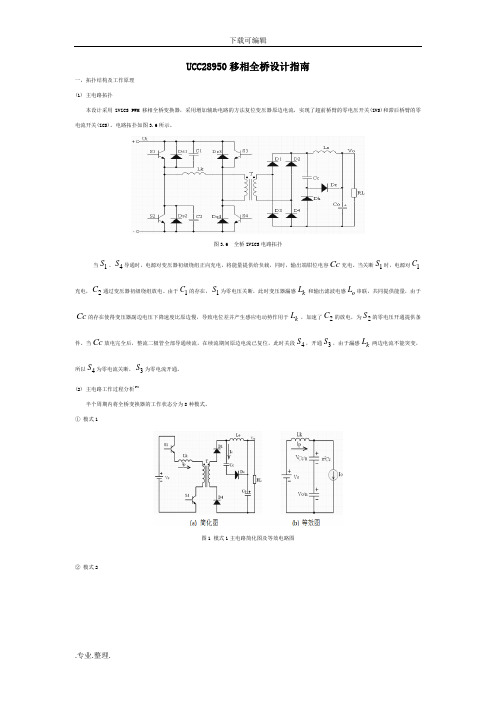
UCC2895移相全桥设计指南一,拓扑结构及工作原理(i)主电路拓扑本设计采用ZVZCS PWM移相全桥变换器,采用增加辅助电路的方法复位变压器原边电流,实现了超前桥臂的零电压开关电流开关(ZCS)。
电路拓扑如图3.6所示图1模式1主电路简化图及等效电路图②模式2当S|、S4导通时,电源对变压器初级绕组正向充电,将能量提供给负载,同时,输出端钳位电容Cc充电。
当关断S时,电源对C i 充电,C2通过变压器初级绕组放电。
由于C1的存在,S|为零电压关断,此时变压器漏感L k和输出滤波电感L o串联,共同提供能量,由于Cc的存在使得变压器副边电压下降速度比原边慢,导致电位差并产生感应电动势作用于L k,加速了C2的放电,为S2的零电压开通提供条件。
当Cc放电完全后,整流二极管全部导通续流,在续流期间原边电流已复位,此时关段S4,开通S3,由于漏感L k两边电流不能突变,所以S4为零电流关断,S3为零电流开通。
(2)主电路工作过程分析[7]半个周期内将全桥变换器的工作状态分为①模式18种模式。
(ZVS)和滞后桥臂的零5图4模式4主电路简化图及等效电路图图5模式5主电路简化图及等效电路图③模式3 ④模式4 14DD图2模式2简化电路图 (1)U 图3模式3简化电路图u⑤模式5Jilin⑥模式6图6模式6主电路简化图及等效电路图⑧模式8图8模式8主电路简化电路图二,关键冋题1:滞后臂较难实现 ZVS原因:滞后臂谐振的时候,次级绕组短路被钳位,所以副边电感无法反射到原边参加谐振,导致谐振的能量只能由谐振电感提供,如果能量不够, 就会出现无法将滞后臂管子并联的谐振电容电压谐振到0V.解决方法:① 、增大励磁电流。
但会增大器件与变压器损耗。
② 、增大谐振电感。
但会造成副边占空比丢失更严重。
③ 、增加辅助谐振网络。
但会增加成本与体积。
⑦模式7 图7模式7主电路简化电路图2,畐V边占空比的丢失原因:移相全桥的原边电流存在着一个剧烈的换流过程,此时原边电流不足以提供副边的负载电流,因此副边电感就会导通另一个二极管续流,即副边处于近似短路状态;Dloss与谐振电感量大小以及负载RL大小成正比,与输入电压大小成反比。
UCC28950移相全桥设计的指南
UCC28950移相全桥设计指南一,拓扑结构及工作原理(1) 主电路拓扑本设计采用ZVZCS PWM移相全桥变换器,采用增加辅助电路的方法复位变压器原边电流,实现了超前桥臂的零电压开关(ZVS)和滞后桥臂的零电流开关(ZCS)。
电路拓扑如图3.6所示。
图3.6 全桥ZVZCS电路拓扑当1S、4S导通时,电源对变压器初级绕组正向充电,将能量提供给负载,同时,输出端钳位电容Cc充电。
当关断1S时,电源对1CC通过变压器初级绕组放电。
由于1C的存在,1S为零电压关断,此时变压器漏感k L和输出滤波电感o L串联,共同提供能量,由于充电,2Cc的存在使得变压器副边电压下降速度比原边慢,导致电位差并产生感应电动势作用于k L,加速了2C的放电,为2S的零电压开通提供条件。
当Cc放电完全后,整流二极管全部导通续流,在续流期间原边电流已复位,此时关段4S,开通3S,由于漏感k L两边电流不能突变,所以4S为零电流关断,3S为零电流开通。
(2) 主电路工作过程分析[7]半个周期内将全桥变换器的工作状态分为8种模式。
①模式1图1 模式1主电路简化图及等效电路图②模式2图2 模式2简化电路图③模式3图3模式3简化电路图④模式4图4模式4主电路简化图及等效电路图⑤模式5图5模式5 主电路简化图及等效电路图⑥模式6图6 模式6主电路简化图及等效电路图⑦模式7图7模式7主电路简化电路图⑧模式8图8 模式8主电路简化电路图二,关键问题1:滞后臂较难实现ZVS原因:滞后臂谐振的时候,次级绕组短路被钳位,所以副边电感无法反射到原边参加谐振,导致谐振的能量只能由谐振电感提供,如果能量不够,就会出现无法将滞后臂管子并联的谐振电容电压谐振到0V.解决方法:①、增大励磁电流。
但会增大器件与变压器损耗。
②、增大谐振电感。
但会造成副边占空比丢失更严重。
③、增加辅助谐振网络。
但会增加成本与体积。
2,副边占空比的丢失原因: 移相全桥的原边电流存在着一个剧烈的换流过程,此时原边电流不足以提供副边的负载电流,因此副边电感就会导通另一个二极管续流,即副边处于近似短路状态;Dloss 与谐振电感量大小以及负载RL 大小成正比,与输入电压大小成反比。
- 1、下载文档前请自行甄别文档内容的完整性,平台不提供额外的编辑、内容补充、找答案等附加服务。
- 2、"仅部分预览"的文档,不可在线预览部分如存在完整性等问题,可反馈申请退款(可完整预览的文档不适用该条件!)。
- 3、如文档侵犯您的权益,请联系客服反馈,我们会尽快为您处理(人工客服工作时间:9:00-18:30)。
-+-VSUCC28950 SLUSA16A–MARCH2010–REVISED JULY2010 Green Phase-Shifted Full-Bridge Controller With Synchronous RectificationCheck for Samples:UCC28950FEATURES APPLICATIONS•Phase-Shifted Full-Bridge Converters •Enhanced Wide Range Resonant Zero VoltageSwitching(ZVS)Capability•Server,Telecom Power Supplies•Industrial Power Systems•Direct Synchronous Rectifier(SR)Control•High-Density Power Architectures•Light-Load Efficiency Management Including•Solar Inverters,and Electric Vehicles –Burst Mode Operation–Discontinuous Conduction Mode(DCM),DESCRIPTIONDynamic SR On/Off Control withProgrammable Threshold The UCC28950enhanced phase-shifted controllerbuilds upon Texas Instrument’s industry standard –Programmable Adaptive DelayUCCx895phase-shifted controller family with •Average or Peak Current Mode Control with enhancements that offer best in class efficiency in Programmable Slope Compensation and today’s high performance power systems.The Voltage Mode Control UCC28950implements advanced control of thefull-bridge along with active control of the •Closed Loop Soft Start and Enable Functionsynchronous rectifier output stage.•Programmable Switching Frequency up to1MHz with Bi-Directional Synchronization The primary-side signals allow programmable delaysto ensure ZVS operation over wide-load current and •(+/-3%)Cycle-by-Cycle Current Limitinput voltage range,while the load current naturally Protection with Hiccup Mode Supporttunes the secondary-side synchronous rectifiers •150-µA Start-Up Current switching delays,maximizing overall system •V DD Under Voltage Lockout efficiency.•Wide Temperature Range-40°C to125°CUCC28950Typical ApplicationPlease be aware that an important notice concerning availability,standard warranty,and use in critical applications of TexasInstruments semiconductor products and disclaimers thereto appears at the end of this data sheet.PRODUCTION DATA information is current as of publication date.Copyright©2010,Texas Instruments Incorporated Products conform to specifications per the terms of the TexasInstruments standard warranty.Production processing does notnecessarily include testing of all parameters.UCC28950SLUSA16A–MARCH2010–REVISED DESCRIPTION(CONT.)The UCC28950also offers multiple light-load management features including burst mode and dynamic SR on/off control when transitioning in and out of Discontinuous Current Mode(DCM)operation,ensuring ZVS operation is extended down to much lighter loads.In addition,the UCC28950includes support for peak current along with voltage mode control,programmable switching frequency up to1MHz and a wide set of protection features including cycle-by-cycle current limit, UVLO and thermal shutdown.A90-degree phase-shifted interleaved synchronized operation can be easily arranged between two converters.The UCC28950is available in TSSOP-24package.ORDERING INFORMATIONTEMPERATURE RANGE,T A=PACKAGE TAPE AND REEL QTY.PART NUMBER T J250UCC28950PW -40°C to125°C Plastic24-pin TSSOP(PW)2000UCC28950PWRABSOLUTE MAXIMUM RATINGSover operating free-air temperature range(unless otherwise noted)(1)(2)PARAMETER VALUE UNITInput supply voltage range,V DD(3)-0.4to20.0OUTA,OUTB,OUTC,OUTD,OUTE,OUTF-0.4to VDD+0.4Inputs voltages on DELAB,DELCD,DELEF,SS/EN,DCM,TMIN,RT,SYNC,RSUM,EA+,EA-,-0.4to VREF+COMP,CS,ADEL,ADELEF0.4VOutput voltage on VREF-0.4to5.6ESD rating,HBM2kESD rating,CDM500Continuous total power dissipation See dissipation rating table Operating virtual junction temperature range,T J-40to150Operating ambient temperature range,T A-40to125°C Storage temperature,T stg-65to150Lead temperature(soldering,10sec.)300(1)Stresses beyond those listed under“absolute maximum ratings”may cause permanent damage to the device.These are stress ratingsonly,and functional operation of the device at these or any other conditions beyond those indicated under“recommended operating conditions”is not implied.Exposure to absolute-maximum-rated conditions for extended periods may affect device reliability.(2)These devices are sensitive to electrostatic discharge;follow proper device handling procedures.(3)All voltages are with respect to GND unless otherwise noted.Currents are positive into,negative out of the specified terminal.SeePackaging Section of the datasheet for thermal limitations and considerations of packages.DISSIPATION RATINGS(1)DERATINGPOWER RATINGFACTORR q JC R q JAPACKAGE(°C/W)(°C/W)ABOVE TA =T A<25°C T A=70°C T A=85°C25°CPW18.589.311.2mW/°C 1.12W0.615W0.448W (1)These thermal data are taken at standard JEDEC test conditions and are useful for the thermal performance comparison of differentpackages.The cooling condition and thermal impedance R q JA of practical design is specific.2Submit Documentation Feedback Copyright©2010,Texas Instruments IncorporatedProduct Folder Link(s):UCC28950UCC28950 SLUSA16A–MARCH2010–REVISED JULY2010RECOMMENDED OPERATING CONDITIONSover operating free-air temperature range(unless otherwise noted)MIN TYP MAX UNIT Supply voltage range,V DD81217V Operating junction temperature range-40125°C Converter switching frequency setting range,F SW(nom)501000kHz Programmable delay range between OUTA,OUTB and OUTC,OUTD set by301000resistors DELAB and DELCD and parameter K A(1)ns Programmable delay range between OUTA,OUTF and OUTB,OUTE set by301400resistor DELEF,and parameter K EF(1)Programmable DCM range as percentage of voltage at CS(1)5%30% Programmable T MIN range100800ns(1)Verified during characterization only.ELECTRICAL CHARACTERISTICS(1)V DD=12V,T A=T J=-40°C to125°C,C VDD=1µF,C REF=1µF,R AB=22.6kΩ,R CD=22.6kΩ,R EF=13.3kΩ,RSUM=124 kΩ,RMIN=88.7kΩ,RT=59kΩconnected between RT pin and5-V voltage supply to set F SW=100kHz(F OSC=200kHz) (unless otherwise noted).All component designations are from the Typical Application Diagram.PARAMETER TEST CONDITION MIN TYP MAX UNITS Under Voltage Lockout(UVLO)UVLO_RStart threshold 6.757.37.9THUVLO_F Minimum operating voltage6.15 6.77.2VTH after startUVLO_HHysteresis0.530.60.75YSTSupply CurrentsI DD(off)Startup current V DD is5.2V150270µAI DD Operating supply current510mA VREF Output VoltageV REF VREF total output range0≤IR≤20mA;V DD=from8V to17V 4.9255 5.075V ISCC Short circuit current VREF=0V-53-23mA Switching Frequency(½of internal oscillator frequency F OSC)F SW(nom)Total range92100108KHzD MAX Maximum duty cycle95%97% SynchronizationRT=59kΩbetween RT and GND;Input pulsesPH SYNC Total range859095°PH200kHz,D=0.5at SYNCRT=59kΩbetween RT and5V;-40°C≤T J≤F SYNC Total range180200220kHz125°CT PW Pulse width 2.2 2.5 2.8µs (1)Typical values for T A=25°CCopyright©2010,Texas Instruments Incorporated Submit Documentation Feedback3Product Folder Link(s):UCC28950UCC28950SLUSA16A–MARCH2010–REVISED ELECTRICAL CHARACTERISTICS(1)(continued)V DD=12V,T A=T J=-40°C to125°C,C VDD=1µF,C REF=1µF,R AB=22.6kΩ,R CD=22.6kΩ,R EF=13.3kΩ,RSUM=124 kΩ,RMIN=88.7kΩ,RT=59kΩconnected between RT pin and5-V voltage supply to set F SW=100kHz(F OSC=200kHz) (unless otherwise noted).All component designations are from the Typical Application Diagram.PARAMETER TEST CONDITION MIN TYP MAX UNITS Error AmplifierV ICM range ensures parameters,the functionalityCommon mode input voltageV ICM ensured for3.6V<V ICM<VREF+0.4V,and-0.40.5 3.6V rangeV<V ICM<0.5VV IO Offset voltage-77mVI BIAS Input bias current-11µAEA HIGH High-level output voltage(EA+)-(EA-)=500mV,I EAOUT=-0.5mA 3.9 4.25VEA LOW Low-level output voltage(EA+)-(EA-)=-500mV,I EAOUT=0.5mA0.250.35I SOURCE Error amplifier source current-8-3.75-0.5mAI SINK Error amplifier sink current 2.7 4.6 5.75I VOL Open-loop dc gain100dB GBW Unity gain bandwidth(2)3MHz Cycle-by-Cycle Current LimitCS pin cycle-by-cycleV CS_LIM 1.942 2.06V thresholdPropagation delay from CS to Input pulse between CS and GND from zero to2.5T CS100ns OUTC and OUTD outputs VInternal Hiccup Mode SettingsDischarge current to setI DS cycle-by-cycle current limit CS=2.5V,VSS=4V152025µAdurationV HCC Hiccup OFF Time threshold 3.2 3.6 4.2VDischarge current to setI HCC 1.90 2.55 3.2µAHiccup Mode OFF TimeSoft Start/EnableI SS Charge current V SS=0V202530µAShutdown/restart/resetV SS_STD0.250.500.70 thresholdVV SS_PU Pull up threshold 3.3 3.7 4.3V SS_CL Clamp voltage 4.20 4.65 4.95(2)Verified during characterization only.4Submit Documentation Feedback Copyright©2010,Texas Instruments IncorporatedProduct Folder Link(s):UCC28950UCC28950 SLUSA16A–MARCH2010–REVISED JULY2010ELECTRICAL CHARACTERISTICS(1)(continued)V DD=12V,T A=T J=-40°C to125°C,C VDD=1µF,C REF=1µF,R AB=22.6kΩ,R CD=22.6kΩ,R EF=13.3kΩ,RSUM=124 kΩ,RMIN=88.7kΩ,RT=59kΩconnected between RT pin and5-V voltage supply to set F SW=100kHz(F OSC=200kHz) (unless otherwise noted).All component designations are from the Typical Application Diagram.PARAMETER TEST CONDITION MIN TYP MAX UNITS Programmable Delay Time Set Accuracy and Range(3)(4)(5)(6)(7)Short delay time set accuracyT ABSET1CS=ADEL=ADELEF=1.8V324556 between OUTA and OUTBLong delay time set accuracyT ABSET2CS=ADEL=ADELEF=0.2V216270325 between OUTA and OUTBShort delay time set accuracyT CDSET1CS=ADEL=ADELEF=1.8V324556 between OUTC and OUTDLong delay time set accuracyT CDSET2CS=ADEL=ADELEF=0.2V216270325 between OUTC and OUTDShort delay time set accuracyT AFSET1CS=ADEL=ADELEF=0.2V223548 between falling OUTA,OUTFLong delay time set accuracyT AFSET2CS=ADEL=ADELEF=1.8V190240290 between falling OUTA,OUTFShort delay time set accuracyT BESET1CS=ADEL=ADELEF=0.2V223548 between falling OUTB,OUTE nsLong delay time set accuracyT BESET2CS=ADEL=ADELEF=1.8V190240290 between falling OUTB,OUTEPulse matching betweenΔT ADBC OUTA rise,OUTD fall and CS=ADEL=ADELEF=1.8V,COMP=2V-50050 OUTB rise,OUTC fallHalf cycle matching betweenΔT ABBA OUTA rise,OUTB rise and CS=ADEL=ADELEF=1.8V,COMP=2V-50050 OUTB rise,OUTA risePulse matching betweenΔT EEFF OUTE fall,OUTE rise and CS=ADEL=ADELEF=0.2V,COMP=2V-60060 OUTF fall,OUTF risePulse matching betweenΔT EFFE OUTE fall,OUTF rise and CS=ADEL=ADELEF=0.2V,COMP=2V-60060 OUTF fall,OUTE rise(3)See Figure3for timing diagram and T ABSET1,T ABSET2,T CDSET1,T CDSET2definitions.(4)See Figure6for timing diagram and T AFSET1,T AFSET2,T BESET1,T BESET2definitions.(5)Pair of outputs OUTC,OUTE and OUTD,OUTF always going high simultaneously.(6)Outputs A or B are never allowed to go high if both outputs OUTE and OUTF are high.(7)All delay settings are measured relatively50%of pulse amplitude.Copyright©2010,Texas Instruments Incorporated Submit Documentation Feedback5Product Folder Link(s):UCC28950UCC28950SLUSA16A–MARCH2010–REVISED ELECTRICAL CHARACTERISTICS(1)(continued)V DD=12V,T A=T J=-40°C to125°C,C VDD=1µF,C REF=1µF,R AB=22.6kΩ,R CD=22.6kΩ,R EF=13.3kΩ,RSUM=124 kΩ,RMIN=88.7kΩ,RT=59kΩconnected between RT pin and5-V voltage supply to set F SW=100kHz(F OSC=200kHz) (unless otherwise noted).All component designations are from the Typical Application Diagram.PARAMETER TEST CONDITION MIN TYP MAX UNITS Light Load Efficiency CircuitV DCM=0.4V,Sweep CS confirm there are OUTEDCM threshold,T=25°C0.370.390.41and OUTF pulsesDCM threshold,T=0°C to V DCM=0.4V,Sweep CS,confirm there are OUTEV DCM0.3640.3900.416V 85°C(8)and OUTF pulsesDCM threshold,T=-40°C to V DCM=0.4V,Sweep CS,confirm there are OUTE0.350.390.43125°C(8)and OUTF pulsesI DCM,SRC DCM Sourcing Current CS<DCM threshold142026µAT MIN Total range R TMIN=88.7kΩ425525625ns OUTPUTS OUTA,OUTB,OUTC,OUTD,OUTE,OUTFI SINK/SRC Sink/Source peak current(8)0.2AT R Rise time C LOAD=100pF925nsT F Fall time C LOAD=100pF725R SRC Output source resistance I OUT=20mA102035ΩR SINK Output sink resistance I OUT=20mA51030 THERMAL SHUTDOWNRising threshold(8)160Falling threshold(8)140°CHysteresis20(8)Verified during characterization only.6Submit Documentation Feedback Copyright©2010,Texas Instruments IncorporatedProduct Folder Link(s):UCC28950UCC28950 SLUSA16A–MARCH2010–REVISED JULY2010DEVICE INFORMATIONTERMINAL FUNCTIONSTERMINALI/O FUNCTIONNUMBER NAME1VREF O5-V,±1.5%,20-mA reference voltage output.2EA+I Error amplifier non-inverting input.3EA-I Error amplifier inverting input.4COMP I/O Error amplifier output and input to the PWM comparator.5SS/EN I Soft-start programming,device enable and hiccup mode protection circuit.6DELAB I Dead-time delay programming between OUTA and OUTB.7DELCD I Dead-time delay programming between OUTC and OUTD.8DELEF I Delay-time programming between OUTA to OUTF,and OUTB to OUTE.9TMIN I Minimum duty cycle programming in burst mode.10RT I Oscillator frequency set.Master or slave mode setting.11RSUM I Slope compensation programming.Voltage mode or peak current mode setting.12DCM I DCM threshold setting.Delay-time programming between primary side and secondary side switches,T AFSET 13ADELEF Iand T BESET.Dead-time programming for the primary switches over CS voltage range,T ABSET and 14ADEL IT CDSET.15CS I Current sense for cycle-by-cycle over-current protection and adaptive delay functions.16SYNC I/O Synchronization out from Master controller to input of slave controller.17OUTF O0.2-A sink/source synchronous switching output.18OUTE O0.2-A sink/source synchronous switching output.19OUTD O0.2-A sink/source primary switching output.20OUTC O0.2-A sink/source primary switching output.21OUTB O0.2-A sink/source primary switching output.22OUTA O0.2-A sink/source primary switching output.23VDD I Bias supply input.24GND Ground.All signals are referenced to this node.Copyright©2010,Texas Instruments Incorporated Submit Documentation Feedback7Product Folder Link(s):UCC28950VDD VREFOUTADELABOUTBADEL OUTCDELCDOUTDOUTEDELEFOUTFADELEFSS/ENCOMP EA-EA+RT RSUM CS SYNCGNDDCMTMIN-V S UCC28950SLUSA16A –MARCH 2010–REVISED JULY 2010Functional Block DiagramTypical Application Diagram8Submit Documentation FeedbackCopyright ©2010,Texas Instruments IncorporatedProduct Folder Link(s):UCC28950UCC28950 SLUSA16A–MARCH2010–REVISED JULY2010Startup Timing DiagramNo output delay shown,COMP-to-RAMP offset not included.Figure1.UCC28950Timing DiagramNOTEThere is no pulse on OUTE during burst mode at startup.Two falling edge PWM pulsesare required before enabling the synchronous rectifier outputs.Copyright©2010,Texas Instruments Incorporated Submit Documentation Feedback9Product Folder Link(s):UCC28950UCC28950SLUSA16A–MARCH2010–REVISED Steady State/Shutdown Timing DiagramNo output delay shown,COMP-to-RAMP offset not included.Figure2.UCC28950Timing Diagram10Submit Documentation Feedback Copyright©2010,Texas Instruments IncorporatedProduct Folder Link(s):UCC28950DETAILED PIN DESCRIPTION AND PARAMETER SETTINGSStart-Up Protection LogicBefore the UCC28950controller will start up,the following conditions must be met:•VDD voltage exceeds rising UVLO threshold7.3V typical.•The5-V reference voltage is available.•Junction temperature is below the thermal shutdown threshold of140°C.•The voltage on the soft-start capacitor is not below0.55V typical.If all those conditions are met,an internal enable signal EN is generated that initiates the soft start process.The duty cycle during the soft start is defined by the voltage at the SS pin,and cannot be lower than the duty cycle set by TMIN,or by cycle-by-cycle current limit circuit depending on load conditions.Voltage Reference(VREF)The accurate(±1.5%)5-V reference voltage regulator with the short circuit protection circuit supplies internal circuitry and provides up to20-mA external output current for setting DC/DC converter parameters.Place low ESR and ESL,preferably ceramic decoupling capacitor C REF in1µF to2.2µF range from this pin to GND as close to the related pins as possible for best performance.The only condition where the reference regulator is shut down internally is during under voltage lockout.Error Amplifier(EA+,EA-,COMP)The error amplifier has two uncommitted inputs,EA+and EA-,with a3-MHz unity bandwidth,which allows flexibility in closing the feedback loop.The EA+is a non-inverting input,the EA-is an inverting input and the COMP is the output of the error amplifier.The input voltage common mode range,where the parameters of error amplifier are guaranteed,is from0.5V to3.6V.The output of the error amplifier is connected internally to the non-inverting input of the PWM comparator.The range of the error amplifier output of0.25V to4.25V far exceeds the PWM comparator input ramp-signal range,which is from0.8V to2.8V.The soft-start signal serves as an additional non-inverting input of the error amplifier.The lower of the two non-inverting inputs of the error amplifier is the dominant input and sets the duty cycle where the output signal of the error amplifier is compared with the internal ramp at the inputs of the PWM comparator.()SS SS(master )T 25A C VNI 0.55´m =+SSSS(slave)T C 20.6825K Ln 20.6VNI 0.55=æö´ç÷--èøSoft Start and Enable (SS/EN)The soft-start pin SS/EN is a multi-function pin used for the following operations:•Closed loop soft start with the gradual duty cycle increase from the minimum set by TMIN up to the steady state duty cycle required by the regulated output voltage.•Setting hiccup mode conditions during cycle-by-cycle over current limit.•On/off control for the converter.During soft start,one of the voltages at the SS/EN or EA+pins,whichever is lower (SS/EN -0.55V)or EA+voltage (see Block Diagram),sets the reference voltage for a closed feedback loop.Both SS/EN and EA+signals are non-inverting inputs of the error amplifier with the COMP pin being its output.Thus the soft start always goes under the closed feedback loop and the voltage at COMP pin sets the duty cycle.The duty cycle defined by COMP voltage can not be shorter than TMIN pulse set by the user.However,if the shortest duty cycle is set by the cycle-by-cycle current limit circuit,then it becomes dominant over the duty cycle defined by COMP voltage or by TMIN block.The soft-start duration is defined by an external capacitor C SS ,connected between SS/EN pin and ground,and the internal charge current that has typical value of 25µA.Pulling the soft-start pin externally below 0.55V shuts down the controller.The release of the soft-start pin enables the controller to start,and if there is no current limit condition,the duty cycle applied to the output inductor gradually increases until it reaches the steady state duty cycle defined by the regulated output voltage of the converter.This happens when the voltage at the SS/EN pin reaches and then exceeds the voltage at EA+pin defined as VNI by 0.55V.Thus for the given soft-start time T SS ,the C SS value can be defined by Equation 1or Equation 2:(1)(2)For example,in Equation 1,if the soft-start time T SS is selected to be 10ms,and the VNI is 2.5V,then the soft-start capacitor C SS is equal to 82-nF.NOTEIf the converter is configured in Slave Mode,make sure you place an 825-k Ωresistor from SS pin to ground.Light-Load Power Saving ModeThe UCD28950offers four different light-load management techniques for improving the efficiency of a power converter over a wide load current range.1.Adaptive Delay,(a)ADEL,which sets and optimizes the dead-time control for the primary switches over wide load currentrange.(b)ADELEF,which sets and optimizes the delay-time control between the primary side switches and thesecondary side switches.2.TMIN,sets the minimum duty cycle as long as the part is not in current limit mode.3.Dynamic synchronous rectifier on/off control in DCM Mode,For increased efficiency at loads.The DCM Mode starts when the voltage at CS pin is lower than the threshold set by the user.In DCM Mode,the synchronous output drive signals OUTE and OUTF are brought down low.4.Burst Mode,for maximum efficiency at very light loads or no load.Burst Mode has an even number of PWM TMIN pulses followed by off time.Transition to the Burst Mode is defined by the TMIN duration set by the user.Adaptive Delay,(Delay between OUTA and OUTB,OUTC and OUTD(DELAB,DELCD,ADEL)) The resistor R AB from the DELAB pin,DELAB to GND,along with the resistor divider R AHI from CS pin to ADEL pin and R A from ADEL pin to GND sets the delay T ABSET between one of outputs OUTA or OUTB going low and another output going high Figure3.Figure3.Delay definitions between OUTA and OUTB,OUTC and OUTDThis delay gradually increases as a function of the CS signal from T ABSET1,which is measured at V CS=1.8V,to T ABSET2,which is measured at the V CS=0.2V.This approach ensures there will be no shoot-through current during the high-side and low-side MOSFET switching and optimizes the delay for ZVS condition over a wide load current range.Depending on the resistor divider R AHI and R A,the proportional ratio between longest and shortest delay is set.The max ratio is achieved by tying the CS and ADEL pins together.If ADEL is connected to GND, then the delay is fixed,defined only by the resistor R AB from DELAB to GND.The delay T CDSET1and T CDSET2 settings and their behaviour for outputs OUTC and OUTD are very similar to the one described for OUTA and OUTB.The difference is that resistor R CD connected between DELCD pin and GND sets the delay T CDSET. Delays for outputs OUTC and OUTD share with the outputs OUTA and OUTB the same CS voltage dependence pin ADEL.ABABSET A 5R T ns 5ns0.15V CS K 1.46æö´=+ç÷+´´èøCDCDSET A 5R T ns 5ns0.15V CS K 1.46æö´=+ç÷+´´èøAA A AHIR K R R =+The delay time T ABSET is defined by the following Equation 3.(3)The same equation is used to define the delay time T CDSET in another leg except R AB is replaced by R CD .(4)In these equations R AB and R CD are in k Ωand CS,the voltage at pin CS,is in volts and K A is a numerical coefficient in the range from 0to 1.The delay time T ABSET and T CDSET are in ns.These equations are empirical and they are approximated from measured data.Thus,there is no unit agreement in the equations.As an example,assume R AB =15k Ω,CS =1V and K A =0.5.Then the T ABSET is going to be 90.25ns.In both Equation 3and Equation 4,K A is the same and is defined as:(5)K A sets how the delay is sensitive to CS voltage variation.If K A =0(ADEL shorted to GND),the delay is fixed.If K A =1(ADEL is tied to CS),the delay is maximum at CS =0.2V and gradually decreases when CS goes up to 1.8V.The ratio between the maximum and minimum delay can be up to 6:1.It is recommended to start by setting K A =0and set T ABSET and T CDSET relatively large using equations or plots in the data sheet to avoid hard switching or even shoot through current.The delay between outputs A,B and C,D set by resistors R AB and R CS accordingly.Program the optimal delays at light load first.Then by changing K A set the optimal delay for the outputs A,B at maximum current.K A for outputs C,D is the same as for A,ually outputs C,D always have ZVS if sufficient delay is provided.NOTEThe allowed resistor range on DELAB and DELCD,R AB and R CD are 13k Ωto 90k Ω.0.02.0CS Voltage -V350 1.0T A B S E T ,T C D S E T -T i m e D e l a y -n sTIME DELAY (R AB =R CD =13k W )vsCS VOLTAGE3001005250150502000.20.40.60.81.21.41.61.8K A =0.0K A =0.1K A =0.25K A =0.50K A =0.75K A =1.00.02.0CS Voltage -V2000 1.0T A B S E T ,T C D S E T -T i m e D e l a y -n sTIME DELAY (R AB =R CD =90k W )vsCS VOLTAGE180060001600100020012000.20.40.60.81.21.41.61.8K A =0.0K A =0.1K A =0.25K A =0.50K A =0.75K A =1.01400800400R A and R AHI define the portion of voltage at pin CS applied to the pin ADEL (See Typical Application Diagram).K A defines how significantly the delay time depends on CS voltage.Ka varies from 0,where ADEL pin is shorted to ground (R A =0)and the delay does not depend on CS voltage,to 1,where ADEL is tied to CS (R AH =0).Setting K A ,R AB and R CD provides the ability to maintain optimal ZVS conditions of primary switches over load current because the voltage at CS pin includes reflected load current to primary side through the current sensing circuit.The plots in Figure 4and Figure 5show the delay time settings as a function of CS voltage and K A for two different conditions:R AB =R CD =13k Ω(Figure 4)and R AB =R CD =90k Ω(Figure 5).Figure 4.Delay Time Set T ABSET and T CDSET(Over CS voltage variation and selected K A for R AB and R CD equal 13k Ω)Figure 5.Delay time set T ABSET and T CDSET(Over CS voltage variation and selected K A for R AB and R CD equal 90k Ω)EFAFSET EF 5R T ns 4ns 2.65V CS K 1.32æöæö´=+ç÷ç÷ç÷-´´èøèøAEFEF AEF AEF(hi)R K R R =+Adaptive Delay (Delay between OUTA and OUTF,OUTB and OUTE (DELEF,ADELEF ))The resistor R EF from the DELEF pin to GND along with the resistor divider R AEFHI from CS pin to ADELEF pin and R AEF from ADELEF pin to GND sets equal delays T AFSET and T BESET between outputs OUTA or OUTB going low and related output OUTF or OUTE going low Figure 6.Figure 6.Delay Definitions Between OUTA and OUTF,OUTB and OUTEThese delays gradually increase as function of CS signal from T AFSET1,which is measured at V CS =0.2V,to T AFSET2,which is measured at V CS =1.8V.Opposite to the DELAB and DELCD behaviour,this delay is longest (T AFSET2)when the signal at CS pin is maximized and shortest (T AFSET1)when the CS signal is minimized.This approach will reduce the synchronous rectifier MOSFET body diode conduction time over a wide load current range thus improving efficiency and reducing diode recovery time.Depending on the resistor divider R AEFHI and R AEF ,the proportional ratio between longest and shortest delay is set.If CS and ADELEF are tied,the ratio is maximized.If ADELEF is connected to GND,then the delay is fixed,defined only by resistor R EF from DELEF to GND.The delay time T AFSET is defined by the following Equation 6.The same defines the delay time T BESET .(6)In this equation R EF is in k Ω,the CS,which is the voltage at pin CS,is in volts and K EF is a numerical gain factorof CS voltage from 0to 1.The delay time T AFSET is in ns.This equation is empirical approximation of measured data,thus,there is no unit agreement in it.As an example of calculation,assume R EF =15k Ω,CS =1V and K EF =0.5.Then the T AFSET is going to be 41.7ns.K EF is defined as:(7)R AEF and R AEFHI define the portion of voltage at pin CS applied to the pin ADELEF (See Typical Application Diagram ).K EF defines how significantly the delay time depends on CS voltage.K EF varies from 0,where ADELEF pin is shorted to ground (R AEF =0)and the delay does not depend on CS voltage,to 1,where ADELEF is tied to CS (R AEFHI =0).NOTEThe allowed resistor range on DELEF,R EF is 13k Ωto 90k Ω.。