S-89210A中文资料
LT8920 数据手册

T8900 Datasheet Revision 1.2LT89202.4G 可变数据率射频芯片1. 模块方框图 (4)2. 极限值 (5)3. 电气特性 (6)4. 典型应用 (9)5. 管脚描述 (10)6. SPI 接口 (12)6.1. SPI 默认格式 (12)6.2. SPI Optional Format (12)6.3. SPI 时序要求 (12)7. IIC 接口 (14)7.1. I2C 命令格式 (14)7.2. I2C 特性 (14)7.3. I2C 器件地址 (15)8. 状态机框图 (16)9. 寄存器信息 (17)9.1. Register 3 – Read only (17)9.2. Register 6 – Read only (17)9.3. Register 7 (17)9.4. Register 9 (18)9.5. Register 10 (18)9.6. Register 11 (18)9.7. Register 23 (18)9.8. Register 27 (19)9.9. Register 29 – Read only (19)9.10. Register 30 – Read only (19)9.11. Register 31 – Read only (19)9.12. Register 32 (20)9.13. Register 33 (22)9.14. Register 34 (22)9.15. Register 35 (22)9.16. Register 36 (23)9.17. Register 37 (23)9.18. Register 38 (24)9.19. Register 39 (24)9.20. Register 40 (24)9.21. Register 41 (24)9.22. Register 42 (25)9.23. Register 43 (25)9.24. Register 48 – Read only (26)9.25. Register 50 (26)9.26. Register 52 (26)10. 寄存器推荐值 (28)11. 注意事项 (29)11.1. 上电和寄存器初始化数据 (29)11.2. 进入sleep mode和唤醒 (30)11.3. 数据包格式 (30)11.4. 清空FIFO指针 (30)11.5. Packet Payload Length (30)11.6. 状态机决定包长度 (32)11.6.1. 发射时序 (32)11.7. 接收时序 (34)11.8. MCU/应用决定包长度 (35)11.8.1. FW_TERM_TX= 1 (36)11.8.2. FW_TERM_TX= 0 (发射状态) (38)11.8.3. FW_TERM_TX= 0 (RX) (40)11.9. 晶体振荡器 (42)11.9.1. Quartz crystal application (42)11.9.2. 外部时钟输入 (42)11.9.3. 减小管脚数 (43)11.9.4. CKPHA (43)12. 封装形式 (44) (45)13. IR Reflow Standard (46)14. 文档更新历史.............................................错误!未定义书签。
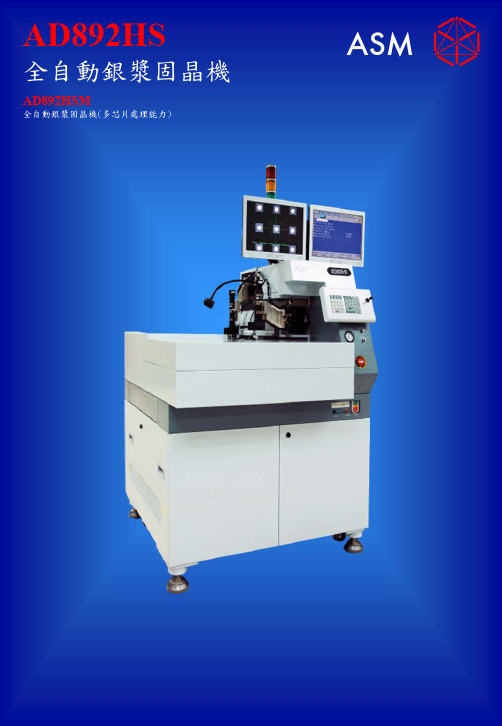
ASM_AD892HS
記憶容量
底板數量 焊點數量/底板
500 2,000
焊頭
吸咀 焊接壓力
表面吸取類形 30 - 250 g
工件工作台
行程範圍 XY分辨率
16” x 4” (406 mm x 101mm) 0.05 mil (1.25µm)
* 機件技術之㈾料,若經修改,怒不另行通知 * 實際表現會因產品而㈲斦改變
芯片系統
Kaohsiung 高雄 Tel : 886-7-367 6300 Fax : 886-7-367 6399
Hsin Chu 新竹 Tel : 886-3-543 1500 Fax : 886-3-543 1555
/
Philippines 菲律賓 Tel : 63-2-850 4543 Fax : 63-2-850 4547
Shenzhen 深圳 Tel : 86-755-8830 8533 Fax : 86-755-8344 6245
China ㆗國 Xiamen 廈門 Tel : 86-592-5509 125 Fax : 86-592-5509 121
Dongguan 東莞 Tel : 86-769-7125 600 Fax : 86-769-7125 601
所需設施
電壓 頻率 壓縮空氣 消耗壓縮空氣 功率消耗
100 - 240 VAC (工廠預先設定) 50/60 Hz (工廠預先設定) 5 bar 180 LPM 1,500 W
體積及重量
AD892HS
寬x深x高 115
ASM
For further information, please contact our regional offices
AD892HS
全㉂動銀漿固晶機
S-80840中文资料

Directions of the IC for taping specifications Product name (abbreviation) Package name (abbreviation) NP: SC-82AB MP: SOT-23-5 UP: SOT-89-3 Y: TO-92 Output type N: Nch open-drain (active low output) L: CMOS (active low output) Detection voltage rank
High-precision detection voltage
±2.0%
Power monitor for microcomputers and reset
CPUs
Low operating voltage
0.7 to 5.0 V Products with detection voltage of 1.4‚uor less 0.95 to 10.0 V Products with a detection voltage of 1.5‚uor more
Features
Applications
1.3 µA typ. (VDD=1.5 V)
Ultra-low current consumption
Products with detection voltage of 1.4 V or less electronic 0.8µA typ. (VDD=3.5 V) Products with detection voltage of 1.5‚uor more
易网
SUPER-SMALL PACKAGE HIGH-PRECISION VOLTAGE DETECTOR
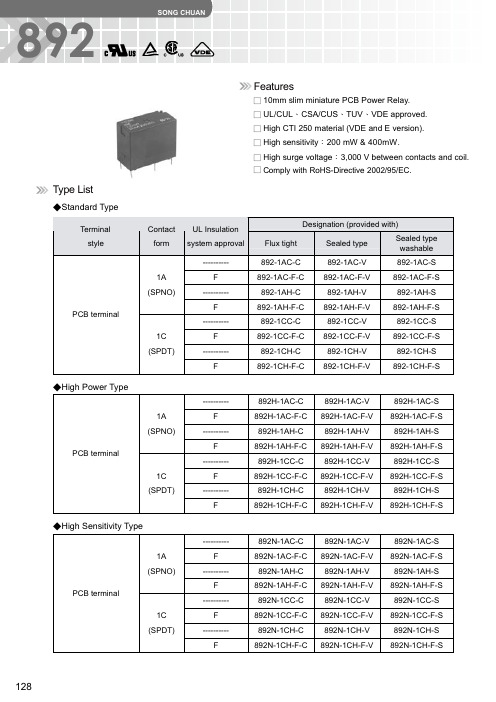
松川继电器892系列

ϬStandard Type
Terminal style
Contact UL Insulation form system approval
----------
Designation (provided with)
892H NO / NCΚ10A/5A 120VAC (50,000 ops.) NO / NCΚ7A/5A 240VAC NO / NCΚ10A/5A 277VAC NO / NCΚ1680VA/1200VA
Coil Rating (DC)
ϬStandard Type
114
Rated Rated current Coil resistance Max. continuous Pick up
F ----------
892-1AH-F-C 892-1CC-C
892-1AH-F-V 892-1CC-V
892-1AH-F-S 892-1CC-S
1C
F
892-1CC-F-C 892-1CC-F-V
892-1CC-F-S
(SPDT)
----------
892-1CH-C
892-1CH-V
892-1CH-S
Contact material Contact resistance (1) Operate time (1) Release time (1) Insulation resistance (1)
AgNi / Ag SnO alloy 100m7����������������������������������������������������������������������������������������������������������������������������������������������������������������������������������������������������������������������������������������������������������������������������������������������������������������������������������������������������������������������������������������������������������������������������������������������������������������������������������������������������������������������������������������������������������������������������������������������������������������������������������������������������������������������������������������������������������������������������������������������������������������������������������������������������������������������������������������������������������������������������������������������������������������������������������������������������������������������������������������������������������������������������������������������������������������������������������������������������������������������������������������������������������������������������������������������������������������������������������������������������������������������������������������������������������������������������������������������������������������������������������������������������������������������������������������������������������������������������������������������������������������������������������������������������������������������������������������������������������������������������������������������������������������������������������������������������������������������������������������������������������������������������������������������������������������������������������������������������������������������������������������������������������������������������������������������������������������������������������������������������������������������������������������������������������������������������������������������������������������������������������������������������������������������������������������������������������������������������������������������������������������������������������������������������������������������������������������������������������������������������������������������������������������������������������������������������������������������������������������������������������������������������������������������������������������������������������������������������������������������������������������������������������������������������������������
892松川系列继电器

30G
Damage limits
100G
Mechanical
10,000,000 operations (frequency 1800 operations/hr)
Electrical
100,000 operations (frequency 900 operations/hr)
-40 ~ +85℃ (no freezing)
10A/5A 125VAC
5A/3A 277VAC
7A/5A 277VAC
TV-3
TUV Pending
TUV
892
892H
7A/3A 120VAC 5A/3A 240VAC
10A/5A 120VAC 7A/5A 240VAC
277VAC NC / NO:1200VA/1680VA
892
COIL DATA (Standard type)
Rated current Coil resistance
Max.
Pickup voltage Dropout voltage Power
Rated voltage ±10% at 25℃ ±10% at 25℃ continuous
36
5.6
6480
SPECIFICATION
Contact resistance Operate time Release time Insulation resistance
Dielectric strength (initial value) Vibration resistance
Shock resistance
3 Blank-Standard type
1CC-SPDT Contact material AgNi10
HZ-892A一体化振动变送器

HZ-892A一体化振动变送器HZ-892A一体化振动变送器1.简介HZ-892A一体化振动变送器:将磁电式振动传感器、精密测量电路集成在一起,构成高精度振动测量系统,该变送器可直接连接DCS、PLC或其它设备,是测量风机、电动机、水泵等工厂设备振动的理想选择。
2.技术参数2.1 频率响应:10 ~ 1000 Hz * 或者5 ~ 1000 Hz(特殊说明)2.2 自振频率:10Hz2.3 量程:振动加速度量程1~5g峰值;振动速度量程0~100mm/s有效值;(可选)常规机械选0-20mm/s,对应输出:4-20mA;振动位移量程0~1900μm峰峰值(可选)风机等设备常用0-200um,对应输出:4-20mA ;2.4 输出电流:4~20mA 2.5输出阻抗:≤500Ω2.6工作电压:DC12-24V±10%2. 7接线方式:二线制2.7最大加速度:10g2.8测量方向:水平或垂直或通用,2.9 使用环境:温度 -40℃~100℃ 相对湿度≤90%2.10 外形尺寸:φ34.1mm×72.4mm2.11 安装螺纹:M10×1.5×10mm(深度)2.12 重量:约324g3.安装3.1 安装位置:垂直或者水平安装于被测振动点上,将传感器底部M10×1.5×10螺钉固定在被测壳体上,然后将传感器拧在上面拧紧即可。
3.2 安装尺寸及规范:参看图一,若变送器安装位置受到高温蒸汽等冲刷时,为降低变送器环境温度、需加防护措施,一般情况下可不加防护。
3.3接线说明:棕色导线接DC24V电源正端,蓝色导线接DC24V电源负端,同时棕色和蓝色导线也是4~20mA输出引线。
连接导线要求有良好的绝缘性能,采用二芯屏蔽电缆。
图一、外形图图二、一体化机壳振动变送器接线图选型举例:(此为机械振动常用选型,安装方式水平,垂直根据机型自定)HZ-892A-S-20V-01-02-00-01-01一体化振动传感器:S为水平安装,量程为0-20mm/s,输出:4-20mA;供电:24V DC;两线制输出2米带航插。
TDA8920B中文资料

TDA8920BJ DBS23P plastic DIL-bent-SIL power package; 23 leads (straight lead length 3.2 mm)
Version SOT566-3
SOT411-1
9397 750 13356
Preliminary data sheet
9397 750 13356
Preliminary data sheet
Rev. 01 — 1 October 2004
© Koninklijke Philips Electronics N.V. 2004. All rights reserved.
3 of 34
Philips Semiconductors
2 × 100 W class-D power amplifier
4. Quick reference data
Table 1: Quick refere
Conditions
General; VP = ±27 V
VP
supply voltage
Iq(tot)
total quiescent supply current
no load; no filter; no RC-snubber network connected
Stereo single-ended configuration
Po
output power RL = 3 Ω; THD = 10 %; VP = ±27 V
DRIVER LOW
TEMPERATURE SENSOR CURRENT PROTECTION VOLTAGE PROTECTION
TDA8920BTH (TDA8920BJ)
892H-1CC-C(松川)
3
66.7
5
40.0
6
33.3
9
22.2
45 80 % of ratHale Waihona Puke d125voltage
180
170 % of
(HN type or
5 % of
1C type only)
405
rated
rated
approx. 0.2W
12
16.7
720
voltage
75 % of
voltage
18
11.1
1620
Dielectric strength (1)
Between open contact : AC 1000V , 50/60Hz 1 min. Between contact and coil : AC 4000V , 50/60Hz 1 min.
Vibration resistance
Operating extremes Damage limit
VDE 40006318
UL / CUL E88991
130
SONG CHUAN
892
Safety Approval Rating
CSA / CUS
892
892H
NOΚ7A 125VAC
NOΚ10A 125VAC
5A 277VAC
7A 277VAC
NCΚ3A 125VAC
TV-3
3A 277VAC
128
SONG CHUAN
本页已使用福昕阅读器进行编辑。
892 福昕软件(C)2005-2007,版权所有,
仅供试用。
Ordering Information
- 1、下载文档前请自行甄别文档内容的完整性,平台不提供额外的编辑、内容补充、找答案等附加服务。
- 2、"仅部分预览"的文档,不可在线预览部分如存在完整性等问题,可反馈申请退款(可完整预览的文档不适用该条件!)。
- 3、如文档侵犯您的权益,请联系客服反馈,我们会尽快为您处理(人工客服工作时间:9:00-18:30)。
Rev.2.1_00
MINI ANALOG SERIES CMOS COMPARATOR
S-89210A/89220A
The mini-analog series is a group of ICs that incorporate a general purpose analog circuit in a small package. The S-89210A/89220A is a CMOS type comparator that has a phase compensation circuit, and that can be driven at a lower voltage with lower current consumption than existing bipolar comparators. These features make this product the ideal solution for small battery-powered portable equipment. The S-89210A/89220A is a single comparator.
Table 6 AC Characteristics (VDD = 5.0 V) Parameter Rise propagation delay time Fall propagation delay time Rise response time Fall response time Symbol tPLH tPHL tTLH tTHL Measurement conditions S-89210A S-89220A S-89210A Overdrive = 100 mV S-89220A CL = 15 pF S-89210A (Refer to Figure 13.) S-89220A S-89210A S-89220A (Ta = 25°C unless otherwise specified) Min. Typ. 45 230 9 45 3 15 3 15 Max. Unit
µs
4
Seiko Instruments Inc.
元器件交易网
MINI ANALOG SERIES Rev.2.1_00
2. VDD = 3.0 V Table 7 DC Characteristics (VDD = 3.0 V) Parameter Symbol Current consumption Input offset voltage Input offset current Input bias current Common-mode input voltage range Maximum output swing voltage Common-mode input signal rejection ratio Power supply voltage rejection ratio Source current Sink current IDD VIO IIO IBIAS VCMR VOH VOL CMRR PSRR ISOURCE ISOURCE ISINK S-89210A S-89220A VOL = 0.5 V IOH = 20 µA IOL = 20 µA VOH = 0 V Measurement Conditions S-89210A S-89220A Min. −4 0 2.7 60 60 120 25 8 (Ta = 25°C unless otherwise specified) Typ. Max. Unit Measurement Circuit 50 120 µA Figure 10 10 30 µA ±3 +4 mV Figure 6 1 pA 1 pA 70 70 2.3 0.01 V V V dB dB µA mA Figure 7 Figure 8 Figure 9 Figure 7 Figure 6 Figure 11 Figure 12
3
元器件交易网
MINI ANALOG SERIES S-89210A/89220A CMOS COMPARATOR Rev.2.1_00
Electrical Characteristics
1. VDD = 5.0 V Table 5 DC Characteristics (VDD = 5.0 V) Parameter Symbol Current consumption Input offset voltage Input offset current Input bias current Common-mode input voltage range Maximum output swing voltage Common-mode input signal rejection ratio Power supply voltage rejection ratio Source current Sink current IDD VIO IIO IBIAS VCMR VOH VOL CMRR PSRR ISOURCE ISINK S-89210A S-89220A VOL = 0.5 V IOH = 20 µA IOL = 20 µA VOH = 0 V Measurement Conditions S-89210A S-89220A Min. −4 0 4.7 60 60 120 25 9 (Ta = 25°C unless otherwise specified) Typ. Max. Unit Measurement Circuit 50 120 µA Figure 10 10 30 µA ±3 +4 mV Figure 6 1 pA 1 pA 70 70 4.3 0.01 V V dB dB µA mA Figure 7 Figure 8 Figure 9 Figure 7 Figure 6 Figure 11 Figure 12
元器件交易网
MINI ANALOG SERIES Rev.2.1_00 Absolute Maximum Ratings
Table 3 Parameter Power supply voltage Input voltage Output voltage Differential input voltage Power dissipation Symbol VDD VIN VOUT VIND PD Ratings VSS−0.3 to VSS+10.0 VSS−0.3 to VSS+7.0 (7.0 max.) VSS−0.3 to VDD+0.3 (7.0 max.) ±7.0 200 (When not mounted on board) 350*1 −40 to +85 −55 to +125 Unit V V V V mW mW °C °C
Features
y Lower operating voltage than the conventional general-purpose comparators: VDD = 1.8 to 5.5 V IDD = 10 µA (S-89220A) y Low input offset voltage: y Lead-free products 4.0 mV (max.) y Low current consumption: IDD = 50 µA (S-89210A)
CMOS COMPARATOR S-89210A/89220A
Operating temperature range Topr Storage temperature range Tstg *1. When mounted on board [Mounted board] (1) Board size : 114.3 mm × 76.2 mm × t1.6 mm (2) Board name : JEDEC STANDAaximum ratings are rated values exceeding which the product could suffer physical damage. These values must therefore not be exceeded under any conditions.
1
元器件交易网
MINI ANALOG SERIES S-89210A/89220A Pin Configuration
SC-88A Top view VDD 5 OUT 4
CMOS COMPARATOR Rev.2.1_00
Table 2 Pin No. 1 2 3 4 5 Symbol IN(+) VSS IN(−) OUT VDD Description Non-inverted input pin GND pin Inverted input pin Output pin Positive power supply pin Internal Equivalent Circuit Figure 3 Figure 3 Figure 2 Figure 4
Recommended Operating Power Supply Voltage Range
Table 4 Parameter Operating power supply voltage range Symbol VDD Range 1.8 to 5.5 Unit V
Seiko Instruments Inc.
Application
y Cellular phones y PDAs y Notebook PCs y Digital cameras y Digital video cameras
Package
Package Name SC-88A Package NP005-B Drawing Code Tape NP005-B Reel NP005-B