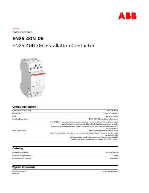
A25L40P(规格书)
EN25-40N-06 安装接触器说明书
1SAA920001-1202 1SAA920000-0705 1SAD938503-0302
1 piece 39 mm 92 mm 69.5 mm
0.24 kg
4013614524554 60 piece 280 mm 210 mm 395 mm
Manual operation is available in 3 states: "On", "Off", "Auto"
4013614524554 1 piece
85365080
2CDC103043M6801
EN25-40N-06
Dimensions
Product Net Width Product Net Height Product Net Depth / Length Product Net Weight
(NO) 25 A
(230 V) Single Phase, NO 5.8 kW (400 V) Three Phase, NO 17.3 kW
(230 V) Single Phase, NO 9 A (400 V) Three Phase, NO 9 A (230 V) Single Phase, NO 1.3 kW (400 V) Three Phase, NO 4 kW
3
AC-3 (NO) 500000 cycle AC-7a (NO) 130000 cycle AC-7b (NO) 500000 cycle
1000000 cycle 4 0
4
2
3 IEC/EN 60947-1 IEC/EN 60947-4-1
IP25 说明书(1)
IP25说明书目录●功能概述……………………………………………………………………….●声明事项……………………………………………………………………….●认识音响……………………………………………………………………….●基本功能………………………………………………………………………开机功能………………………………………………………………………播放功能………………………………………………………………………TUNE………………………………………………………………………………IPHONE……………………………………………………………………………IPHONE来电提示功能…………………………………………………………..AUX……………………………………………………………………………暂停功能………………………………………………………………………上下选曲功能…………………………………………………………………快退/快进功能…………………………………………………………………音量调节………………………………………………………………………电池功能……………………………………………………………………..时钟设置………………………………………………………………………..闹钟设置……………………………………………………………………….闹钟贪.睡………………………………………………………………………睡眠设置………………………………………………………………………●遥控按键功能:………………………………………………………………...●维修指南及疑难解答……………………………………………………………●规格说明………………………………………………………………………....●介绍感谢尊贵的您选购我们的新一代多功能组合迷你音响!此款组合迷你音响,具有多种功能复合,本机完美的音质、及极高的可靠性和精巧的外观相得益彰,堪称大师级的作品,衷心的希望能给喜欢音乐的您带来数码时代的超凡享受。
TA25DU过载保护器说明书

Overload Selection
Order references
Overload rating Full load A
Approximate motor rating
400V/3PH AC3
230V/1PH
Recommended max. fuse size for short circuit protection A
95
96 A2
C
Stop/reset
A1 1
Remote stop
95
Reset 96
A2 C
A1 1
L1
L1
Remove link
A knockout is provided in the lid of the DOL for an extra control device.
1. Remove lid of starter
Trip class 10 requirements IEC 947-4-1
1.05 x FLC 1.2 x FLC 1.5 x FLC 7.2 x FLC
No tripping Trip within 2 hours Trip within 4 minutes Trip between 4s and 10s
TA25DU1.4 TA25DU1.8 TA25DU2.4 TA25DU3.1 TA25DU4.0 TA25DU6.5 TA25DU11 TA25DU14 TA25DU19 TA25DU25 TA25DU32
Min. Max. kW
hp
kW
hp
1.0
1.4
0.37 0.55 0.07 0.09 4
1.3
For further information please contact your ABB Technical Helpline 02476 368500
SPI700A+
SPI Flash量产型专用编程器SPI 700A+使用说明书一、 产品简介:1. 本编程器使用从SD\MMC卡读取文件并编程的独特的编程方式,省去制作母片的步骤;同时也可以工作于1到7的IC拷贝模式。
2. 软件自动升级,通过在SD\MMC卡中放入功升级文件完成对产品软件的更新,添加对新型号SPI Flash的支持。
3. 本机提供一个以 “Versatile” 命名的万用IC型号对于大多数SPI Flash在以卡为数据源时都可以使用此型号拷贝。
4. 方便的文件上传功能,直接把SPI Flash中数据保存到SD\MMC卡。
5. 累计拷贝成功的IC数目显示功能,方便批量生产计数。
二、 功能说明:提示:A、母片的放置位置在【P&B】即8号IC座。
B、 拷贝的数据源:如果您插卡则数据源为卡,否则为母片。
C、 下文中提到的“同时按两个按键”是指在第一个按键按下后保持不松,再按下第二个键(即只要出现两个按键在某一时刻都处于按下状态)。
按键功能:1. 确定\自动:在空闲状态按此键开始自动拷贝,工作的顺序为(擦除→编程→校验),如果在此过程中检测到错误对应IC的指示灯将点亮(如果使用母片则其指示灯为常亮)。
校验结束后显示屏右下角将显示累计拷贝成功的IC数目,每次使用“文件选择”功能后计数将清零。
2. 下一个\软验(校验):在空闲状态按此键开始校验,如果在此过程中检测到错误对应IC的指示灯将点亮(如果使用母片则其指示灯为常亮)。
“校验”功能不影响拷贝成功IC计数。
3. 上一个\拷贝:在空闲状态按此键开始拷贝,拷贝前本机将检测芯片是否为空,如果不为空则进行擦除。
拷贝完成后如果当前文件是第一次进行拷贝,将进行校验以排出文件损坏的问题。
在此过程中检测到错误对应IC的指示灯将点亮(如果使用母片则其指示灯为常亮)。
拷贝结束后显示屏右下角将显示累计拷贝成功的IC数目,每次使用“文件选择”功能后计数将清零。
4. 文件选择:在空闲状态并已经插卡同时按【下一个】和【上一个】键将进入【文件选择】模式,此时显示屏第一行显示按【确定】键将执行的命令,显示屏第二行显示根目录,或上一次使用过的文件名。
fl2-40p电风扇说明书

fl2-40p电风扇说明书本扇特点本扇打破了传统落地式电风扇底座型式,其款式新颖,结构合理,外型美观,具有俯仰角度调节,三档变速或定时等功能,送风范围广,使用安全可靠。
技术指标电源种类:单相交流。
额定电压:220V,额定频率:50Hz输入总功率:60W扇叶直径:400mm,输出风量:65m/min。
清洁与贮存1.电风扇清洁前,务必切断电源并拔出电源线插头。
2.按组装相反之程序拆下电风扇零部件。
3.用棉质软布及非溶剂清洁剂除去零部件表面污渍。
切勿用汽油、松香水、去污粉、碱性洗涤剂擦洗风扇,否则会使风扇变色、变形、开裂。
4.切勿将电扇置于水中清洗。
5.电风扇长期不用时,需将风扇表面弄干后包装好,置于干燥环境中。
特别注意事项1.为确保安全,请于安装、使用前认真阅读说明书。
2,开启产品包装后,检查有无异样。
3,勿将包装件留给小孩和老弱病残者。
4.连接电源前,检查使用电源是否与电风扇规格相符。
5,尽量避免使用附加多联插座和加长线。
如有必要该零件必须与电风扇使用安全规定相符。
6,该电风扇仅限于室内使用,避免浴室使用。
7,任何其它使用将被视为不妥当及当然之危险行为。
因使用不当而造成之任何损坏,本公司修理时将追加服务费。
8,电扇运转时勿用手指、铅笔及其它类似物插入电扇网罩内。
9,勿用湿手、湿脚触及电风扇。
10,禁止拉扯电扇及其电源线以切断电源。
12.请勿将电扇置于窗外或室外使用,意外的天气可能造成电扇遭受雨淋、日晒及雷击等损坏之危险。
13.移动、清洁、送修前,必须切断电源,拔出电源线插头。
14,出现质量问题时,请关闭电源,切勿继续使用,并联络售后服务中心检修。
15,电风扇使用场所经常保存说明书。
使用说明1.开机、风量设定:接通电源,按“风量/开”按钮,电风扇开始工作,为“弱”风档。
通过按“风量/开”按钮,可控制风量的强弱,每按一次,风量会在“弱”、“中”、“强”档之间切换一次,同时相应的风量指示灯亮。
2.风类选择:通过按“风类”按钮可选择不同的风类方式(正常风、自然风、和睡眠风)。
25AA640中文资料

I/O Control Logic
Memory
X
Control
Logic
Dec
EEPROM Array
Page Latches
SI SO
CS SCK HOLD WP
VCC VSS
Y Decoder
Sense Amp. R/W Control
*25xx640 is used in this document as a generic part number for the 25AA640/25LC640/25C640 devices. SPI is a trademark of Motorola.
Input
0.5 VCC
Output
0.5 VCC
Note 1: For VCC ≤ 4.0V
2: For VCC > 4.0V
TABLE 1-2: DC CHARACTERISTICS
All parameters apply over the Commercial (C): Tamb = 0°C to +70°C
*Notice: Stresses above those listed under ‘Maximum ratings’ may cause permanent damage to the device. This is a stress rating only and functional operation of the device at those or any other conditions above those indicated in the operational listings of this specification is not implied. Exposure to maximum rating conditions for an extended period of time may affect device reliability
M25P40中文资料
2.1 连续数输出 (Q) . . . . . . . . . . . . . . . . . . . . . . . . . . . . . . . . . . . . . . . . 8 2.2 连续数输入(D) . . . . . . . . . . . . . . . . . . . . . . . . . . . . . . . . . . . . . . . . . 8 2.3 连续时钟 (C) . . . . . . . . . . . . . . . . . . . . . . . . . . . . . . . . . . . . . . . . . . . . . 8 2.4 器件选择 (S) . . . . . . . . . . . . . . . . . . . . . . . . . . . . . . . . . . . . . . . . . . . . . . 8 2.5 暂停 (HOLD) . . . . . . . . . . . . . . . . . . . . . . . . . . . . . . . . . . . . . . . . . . . . . . . . 8 2.6 写保护(W) . . . . . . . . . . . . . . . . . . . . . . . . . . . . . . . . . . . . . . . . . . . . 8 2.7 驱动电源电压 . . . . . . . . . . . . . . . . . . . . . . . . . . . . . . . . . . . . . . . . . . . 9 2.8 电源地. . . . . . . . . . . . . . . . . . . . . . . . . . . . . . . . . . . . . . . . . . . . . . . . . 9
VLF4012AT-4R7M1R1;VLF4012AT-100MR79;VLF4012AT-3R3M1R3;VLF4012AT-2R2M1R5;中文规格书,Datasheet资料
Inductance tolerance(%) ±30 ±20 ±20 ±20 ±20 ±20 ±20
Test frequency (kHz) 100 100 100 100 100 100 100
DC resistance( ) max. 0.054 0.1 0.15 0.2 0.31 0.46 1.20 typ. 0.047 0.091 0.13 0.1R7
2.8±0.2
1.4max. Dimensions in mm
RECOMMENDED PC BOARD PATTERN
1.2 2.1 3.4 Dimensions in mm
Inductance [at 1/2 Idc1]3 (µH) 1 2.2 3.3 4.7 6.8 10 22
• All specifications are subject to change without notice.
/
001-04 / 20120310 / e531_vlf
(3/17)
Inductors for Power Circuits Wound/STD • Magnetic Shielded
Part No. VLF3014AT-1R0N1R7 VLF3014AT-2R2M1R2 VLF3014AT-3R3M1R0 VLF3014AT-4R7MR90 VLF3014AT-6R8MR72 VLF3014AT-100MR59 VLF3014AT-220MR37
1
SHAPES AND DIMENSIONS
VLF-MT Series VLF302510MT
With the VLF302510MT Series, a DC to DC converter with topclass voltage conversion efficiency for similar size products was achieved by optimizing the magnetic material and configuration. These products are optimal for use as choke coils in switching power supplies such as those in mobile devices requiring spacesaving design. FEATURES • Miniature size Mount area: 3.02.5mm Low profile: 1.0mm max. height • Generic use for portable DC to DC converter line. • High magnetic shield construction should actualize high resolution for EMC protection. • The products contain no lead and also support lead-free soldering. • The products is halogen-free. • It is a product conforming to RoHS directive. APPLICATIONS Smartphones, cellular phones, DSCs, DVCs, HDDs, LCD displays, compact power supply modules, etc. SHAPES AND DIMENSIONS
常用场效应管(25N120等)参数及 代换
常用场效应管(25N120等)参数及代换FGA25N120AND (IGBT) 1200V/25A//TO3P (电磁炉用)FQA27N25 (MOSFET) 250V/27A/TO3P IRFP254FQA40N25 (MOSFET) 250V/40A/280W/0.051Ω/TO3P IRFP264FQA55N25 (MOSFET) 250V/55A/310W/0.03Ω/TO3PFQA18N50V2 (MOSFET) 500V/20A/277W/0.225Ω IRFP460AFQA24N50 (MOSFET) 500V/24A/290W/0.2Ω/TO3PFQA28N50 (MOSFET) 500V/28.4A/310W/0.126Ω/TO3P MTY30N50E FQL40N50 (MOSFET) 500V/40A/560W/0.085Ω/TO264 IRFPS37N50 FQA24N60 (MOSFET) 600V/24A/TO3PFQA10N80 (MOSFET) 800V/9.8A/240W/0.81Ω/TO3PFQA13N80 (MOSFET) 800V/13A/300W/0. Ω/TO3PFQA5N90 (MOSFET) 900V/5.8A/185W/2.3Ω/TO3PFQA9N90C (MOSFET) 900V/8.6A/240W/1.3Ω/TO3PFQA11N90C (MOSFET) 900V/11.4A/300W/0.75Ω/TO3PFFA30U20DN (快恢复二极管) 200V/2×30A/40ns/TO3P DSEK60-02A FFPF30U60S (快恢复二极管) 600V/30A/90ns/TO220F MUR1560FFA30U60DN (快恢复二极管) 600V/2×30A/90ns/TO3P DSEK60-06A MBRP3010NTU (肖特基) 100V/30A/TO-220MBRA3045NTU (肖特基) 45V/30A/TO-3PISL9R3060G2 (快恢复二极管) 600V/30A/35ns/200W/TO247 APT30D60BRHRG3060 (快恢复二极管) 600V/30A/35nS/TO247FQP44N10 (MOSFET) 100V/44A/146W/0.0396Ω/TO220 IRF3710/IRF540NFQP70N10 (MOSFET) 100V/57A/160W/0.025Ω/TO220IRFP450B (MOSFET) 500V/14A/0.4Ω/205W/TO3PIRFP460C (MOSFET) 500V/20A/0.2~0.24Ω/235W IRFP460KA3162/FAN8800 (Drive IC) 单IGBT/MOSFETFET驱动ICRHRP860 (快恢复二极管) 600V/8A/30NS/TO-220 MUR860RHRP1560 (快恢复二极管) 600V/15A/TO0220 MUR1560RHRP8120 (快恢复二极管) 1200V/8A/75W/TO220RHRP15120 (快恢复二极管) 1200V/15A/TO220RHRP30120 (快恢复二极管) 1200V/30A/125W/TO220单 DSEI20-10A RHRG30120 (快恢复二极管) 1200V/30A/T03PSSH45N20B (MOSFET) 200V/45A/TO3P IRFP260FGL40N150D (IGBT) 1500V/40A/TO264快速IGBTFGL60N100BNTD (IGBT) 1000V/60A/TO264快速IGBT 1MBH60-100 HGTG10N120BND (IGBT) 1200V/35A/298W/100ns/TO247HGTG11N120CND (IGBT) 1200V/43A/298W/TO247HGTG18N120BND (IGBT) 1200V/54A/390W/90ns/TO247FQP5N50C (MOSFET) 500V/5A/73W/1.4Ω/TO-220 替代:IRF830,用于35WFQPF5N50C (MOSFET) 500V/5A/38W/1.4Ω/TO-220F 替代:IRF830,用于35WFQP9N50C (MOSFET) 500V/9A/135W/0.6Ω/TO220 替代:IRF840,用于75WFQPF9N50C (MOSFET) 500V/9A/44W/0.6Ω/TO-220F 替代:IRF840,用于75WFQP13N50 (MOSFET) 500V/13.4A/190W/0.43Ω/TO220 用于75W/125W 产品FQPF13N50 (MOSFET) 500V/13.4A/48W/0.43Ω/TO220F 用于75W/125W 产品FQD5N50C (MOSFET) 500V/5A/1.4Ω/TO252 用于35WFQA16N50 (MOSFET) 500V/16A/200W/0.32C/TO3P 用于150W到250W的产品FDP15N50 (MOSFET) 500V/15A/0.43Ω/56W/TO220 用于150W左右的产品FQP18N50V2 (MOSFET) 500V/18A/0.43Ω/208W/TO220 用于250WG到400W的产品FQPF18N50V2 (MOSFET) 500V/18A/0.43Ω/56W/TO220 用于250WG到400W的产品FQA18N50V2 (MOSFET) 500V/20A/277W/0.225Ω/TO3P 用于250WG到400W的产品FQA24N50 (MOSFET) 500V/24A/290W/0.2Ω/TO3P 用于400W的产品FQA24N60 (MOSFET) 600V/23.5A/310W/0.24Ω/TO3P 用于400W的产品FQA28N50 (MOSFET) 500V/28.4A/310W/0.126Ω/TO3P 用于400W的产品FQL40N50 (MOSFET) 500V/40A/560W/0.085Ω/TO264 用于560W的产品IRF740B (MOSFET) 400V/10A/0.55Ω/134W/TO220IRF730B (MOSFET) 400V/5.5A/1.0Ω/73W/TO220IRF830B (MOSFET) 500V/4.5A/1.5Ω/73W/TO220IRF840B (MOSFET) 500V/8A/0.85Ω/134W/TO220IRFP450B (MOSFET) 500V/14A/0.4Ω/205W/TO3PIRFP460C (MOSFET) 500V/20A/0.2~0.24Ω/235WFQPF5N60C (MOSFET) 600V/5A/TO220FFQPF8N60C (MOSFET) 600V/8A/TO220FFQPF10N60C (MOSFET) 600V/10A/TO220FQPF12N60 (MOSFET) 600V/12A/51W/0.65Ω/TO220FFCP11N60 (MOSFET) 650V/11A/125W0.32Ω/TO220RHRD660S (快恢复二极管) 600V/6A/TO-252RHRP860 (快恢复二极管) 600V/8A/75W/TO-220RHRP1560 (快恢复二极管) 600V/15A/TO-220单2N7002 (三极管) 60V/0.12A/SOT-23HUF76629D3S (MOSFET) 100V/20A/110W/TO-252 HUF75639S3S (MOSFET) 100V/56A/200W/TO-263ISL9V3040D3S (IGBT) 430V/21A/150W/300MJ/TO252 ISL9V3040S3S (IGBT) 430V/21A/150W/300MJ/TO263 ISL9V5036S3S (IGBT) 360V/46A/250W/TO262FQP33N10L (MOSFET) 100V/33A/52MΩ127W/TO220。
40n25场效应管参数
40n25场效应管参数
场效应管(FET)是一种三端器件,其中包括栅极、漏极和源极。
它的特性由许多参数描述,其中一些包括:
1. 饱和漏极电流(IDSS),这是在栅极和源极之间施加零电压时,漏极电流的最大值。
2. 饱和漏极电压(Vp),这是在栅极和源极之间的电压,当漏
极电流达到IDSS时。
3. 转导导纳(gm),这是指在特定工作点处,漏极电流与栅极
-源极电压之间的变化率。
4. 截止电压(VGS(off)),这是栅极-源极电压,当漏极电流
为零时。
5. 输出电导(rd),这是指在特定工作点处,漏极-源极电压
与漏极电流之间的变化率。
6. 输入电阻(Rin),这是指FET的输入端(栅极)的电阻,
通常是指在特定工作点处的值。
这些参数可以根据特定的FET型号和制造商而有所不同。
因此,如果你有特定的FET型号,我可以帮助你找到更准确的参数数值。
- 1、下载文档前请自行甄别文档内容的完整性,平台不提供额外的编辑、内容补充、找答案等附加服务。
- 2、"仅部分预览"的文档,不可在线预览部分如存在完整性等问题,可反馈申请退款(可完整预览的文档不适用该条件!)。
- 3、如文档侵犯您的权益,请联系客服反馈,我们会尽快为您处理(人工客服工作时间:9:00-18:30)。
4 Mbit, Low Voltage, Serial Flash Memory Preliminary With 50MHz SPI Bus InterfaceDocument Title4 Mbit, Low Voltage,Serial Flash Memory With 50MHz SPI Bus InterfaceRevision HistoryDate Remark Rev. No. History Issue0.0 Initial issue March 17, 2006 Preliminary0.1 Add the Fast Read Dual Operation Instruction April 4, 2006Add QFN 8L (5 x 6mm) package type0.2 Add QFN 8L (5 x 6mm) package outline dimensions April 20, 20064 Mbit, Low Voltage, Serial Flash MemoryPreliminaryWith 50MHz SPI Bus InterfaceFEATURES4 Mbit of Flash MemoryFlexible Sector Architecture (4/4/8/16/32)KB/64x7 KB Bulk Erase (4 Mbit) in 6s (typical) Sector Erase (512 Kbit) in 1s (typical)Page Program (up to 256 Bytes) in 3ms (typical) 2.7 to 3.6V Single Supply Voltage SPI Bus Compatible Serial Interface 50MHz Clock Rate (maximum)Fast Read Dual Operation Instruction (3Bh/BBh) Deep Power-down Mode 1µA (typical) Electronic Signatures- JEDEC Standard two-Byte Signature (2013h)- RES Instruction, One-Byte, Signature (12h), for backward compatibility GENERAL DESCRIPTIONThe A25L40P is a 4 Mbit (512K x 8) Serial Flash Memory, with advanced write protection mechanisms, accessed by a high speed SPI-compatible bus.The memory can be programmed 1 to 256 bytes at a time, using the Page Program instruction.The memory is organized as 16 sectors, each containing 256 pages. Each page is 256 bytes wide. Thus, the whole memory can be viewed as consisting of 2048 pages, or 524,288 bytes. The whole memory can be erased using the Bulk Erase instruction, or a sector at a time, using the Sector Erase instruction.Pin ConfigurationsSO8 Connections SO16 ConnectionsNote:DU = Do not UseQFN8 ConnectionsBlock DiagramD QC HOLDWSPin DescriptionsLogic SymbolSSVSIGNAL DESCRIPTIONSerial Data Output (Q). This output signal is used to transfer data serially out of the device. Data is shifted out on the falling edge of Serial Clock (C).Serial Data Input (D). This input signal is used to transfer data serially into the device. It receives instructions, addresses, and the data to be programmed. Values are latched on the rising edge of Serial Clock (C).Serial Clock (C). This input signal provides the timing of the serial interface. Instructions, addresses, or data present at Serial Data Input (D) are latched on the rising edge of Serial Clock (C). Data on Serial Data Output (Q) changes after the falling edge of Serial Clock (C).Chip Select (S). When this input signal is High, the device is deselected and Serial Data Output (Q) is at high impedance. Unless an internal Program, Erase or Write Status Register cycle is in progress, the device will be in the Standby mode (this is not the Deep Power-down mode). Driving Chip Select (S) Low enables the device, placing it in the active power mode.After Power-up, a falling edge on Chip Select (S) is required prior to the start of any instruction.Hold (HOLD). The Hold (HOLD) signal is used to pause any serial communications with the device without deselecting the device.During the Hold condition, the Serial Data Output (Q) is high impedance, and Serial Data Input (D) and Serial Clock (C) are Don’t Care. To start the Hold condition, the device must be selected, with Chip Select (S) driven Low.Write Protect (W). The main purpose of this input signal is to freeze the size of the area of memory that is protected against program or erase instructions (as specified by the values in the BP2, BP1 and BP0 bits of the Status Register).SPI MODESThese devices can be driven by a microcontroller with its SPI peripheral running in either of the two following modes:– CPOL=0, CPHA=0– CPOL=1, CPHA=1For these two modes, input data is latched in on the rising edge of Serial Clock (C), and output data is available from the falling edge of Serial Clock (C).The difference between the two modes, as shown in Figure 2, is the clock polarity when the bus master is in Stand-by mode and not transferring data:– C remains at 0 for (CPOL=0, CPHA=0)– C remains at 1 for (CPOL=1, CPHA=1)Figure 1. Bus Master and Memory Devices on the SPI BusNote: The Write Protect (W ) and Hold (HOLD ) signals should be driven, High or Low as appropriate.Figure 2. SPI Modes SupportedC CD Q0011CPOL CPHAOPERATING FEATURESPage ProgrammingTo program one data byte, two instructions are required: Write Enable (WREN), which is one byte, and a Page Program (PP) sequence, which consists of four bytes plus data. This is followed by the internal Program cycle (of duration t PP).To spread this overhead, the Page Program (PP) instruction allows up to 256 bytes to be programmed at a time (changing bits from 1 to 0), provided that they lie in consecutive addresses on the same page of memory.Sector Erase and Bulk EraseThe Page Program (PP) instruction allows bits to be reset from 1 to 0. Before this can be applied, the bytes of memory need to have been erased to all 1s (FFh). This can be achieved, a sector at a time, using the Sector Erase (SE) instruction, or throughout the entire memory, using the Bulk Erase (BE) instruction. This starts an internal Erase cycle (of duration t SE or t BE).The Erase instruction must be preceded by a Write Enable (WREN) instruction.Polling During a Write, Program or Erase CycleA further improvement in the time to Write Status Register (WRSR), Program (PP) or Erase (SE or BE) can be achieved by not waiting for the worst case delay (t W, t PP, t SE, or t BE). The Write In Progress (WIP) bit is provided in the Status Register so that the application program can monitor its value, polling it to establish when the previous Write cycle, Program cycle or Erase cycle is complete.Active Power, Stand-by Power and DeepPower-Down ModesWhen Chip Select () is Low, the device is enabled, and in the Active Power mode.When Chip Select (S) is High, the device is disabled, but could remain in the Active Power mode until all internal cycles have completed (Program, Erase, Write Status Register). The device then goes in to the Stand-by Power mode. The device consumption drops to I CC1.The Deep Power-down mode is entered when the specific instruction (the Enter Deep Power-down Mode (DP) instruction) is executed. The device consumption drops further to I CC2. The device remains in this mode until another specific instruction (the Release from Deep Power-down Mode and Read Electronic Signature (RES) instruction) is executed.All other instructions are ignored while the device is in the Deep Power-down mode. This can be used as an extra software protection mechanism, when the device is not in active use, to protect the device from inadvertent Write, Program or Erase instructions. Status RegisterThe Status Register contains a number of status and control bits that can be read or set (as appropriate) by specific instructions.WIP bit. The Write In Progress (WIP) bit indicates whether the memory is busy with a Write Status Register, Program or Erase cycle.WEL bit. The Write Enable Latch (WEL) bit indicates the status of the internal Write Enable Latch, BP2, BP1, and BP0 bits. The Block Protect (BP2, BP1, BP0) bits are non-volatile. They define the size of the area to be software protected against Program and Erase instructions.SRWD bit. The Status Register Write Disable (SRWD) bit is operated in conjunction with the Write Protect (W) signal. TheStatus Register Write Disable (SRWD) bit and Write Protect (W) signal allow the device to be put in the Hardware Protected mode. In this mode, the non-volatile bits of the Status Register (SRWD, BP2, BP1, BP0) become read-only bits.Protection ModesThe environments where non-volatile memory devices are used can be very noisy. No SPI device can operate correctly in the presence of excessive noise. To help combat this, the A25L40P boasts the following data protection mechanisms:Power-On Reset and an internal timer (t PUW) can provide protection against inadvertant changes while the power supply is outside the operating specification.Program, Erase and Write Status Register instructions are checked that they consist of a number of clock pulses that is a multiple of eight, before they are accepted for execution.All instructions that modify data must be preceded by a Write Enable (WREN) instruction to set the Write Enable Latch (WEL) bit. This bit is returned to its reset state by the following events:- Power-up- Write Disable (WRDI) instruction completion- Write Status Register (WRSR) instruction completion- Page Program (PP) instruction completion- Sector Erase (SE) instruction completion- Bulk Erase (BE) instruction completionThe Block Protect (BP2, BP1, BP0) bits allow part of the memory to be configured as read-only. This is the Software Protected Mode (SPM).The Write Protect (W) signal allows the Block Protect (BP2, BP1, BP0) bits and Status Register Write Disable (SRWD) bit to be protected. This is the Hardware Protected Mode (HPM).In addition to the low power consumption feature, the Deep Power-down mode offers extra software protection from inadvertant Write, Program and Erase instructions, as all instructions are ignored except one particular instruction (the Release from Deep Power-down instruction).Table 1. Protected Area SizesStatus Register Content Memory ContentBP2 BitBP1 Bit BP0 BitProtected AreaUnprotected Area0 0 0 noneAll sectors 1 (sixteen sectors: 0 to 7) 0 0 1 Upper eighth (sector 7)Lower seven-eighths (fifteen sectors: 0 to 6) 0 1 0 Upper quarter (two sectors: 6 and 7) Lower three-quarter (fourteen sectors: 0 to 5) 0 1 1 Upper half (four sectors: 4 to 7) Lower half (twelve sectors: 0 to 3) 1 0 0 All sectors (eight sectors: 0 to 7) none 1 0 1 All sectors (sixteen sectors: 0 to 7) none 1 1 0 All sectors (sixteen sectors: 0 to 7) none 111All sectors (sixteen sectors: 0 to 7)noneNote: 1. The device is ready to accept a Bulk Erase instruction if, and only if, all Block Protect (BP2, BP1, BP0) are 0.2. The sector 0 include sector 0-0, sector 0-1, sector 0-2 and sector 0-3.Hold ConditionThe Hold (HOLD ) signal is used to pause any serial communications with the device without resetting the clocking sequence. However, taking this signal Low does not terminate any Write Status Register, Program or Erase cycle that is currently in progress.To enter the Hold condition, the device must be selected, with Chip Select (S ) Low.The Hold condition starts on the falling edge of the Hold (HOLD ) signal, provided that this coincides with Serial Clock (C) being Low (as shown in Figure 3.).The Hold condition ends on the rising edge of the Hold (HOLD ) signal, provided that this coincides with Serial Clock (C) being Low.If the falling edge does not coincide with Serial Clock (C) being Low, the Hold condition starts after Serial Clock (C) next goes Low. Similarly, if the rising edge does not coincide with Serial Clock (C) being Low, the Hold condition ends after Serial Clock (C) next goes Low. This is shown in Figure 3.During the Hold condition, the Serial Data Output (Q) is high impedance, and Serial Data Input (D) and Serial Clock (C) are Don’t Care.Normally, the device is kept selected, with Chip Select (S ) driven Low, for the whole duration of the Hold condition. This is to ensure that the state of the internal logic remains unchanged from the moment of entering the Hold condition.If Chip Select (S ) goes High while the device is in the Hold condition, this has the effect of resetting the internal logic of the device. To restart communication with the device, it is necessary to drive Hold (HOLD ) High, and then to drive Chip Select (S ) Low. This prevents the device from going back to the Hold condition.Figure 3. Hold Condition Activation(standard use)HOLDC Condition(non-standard use)MEMORY ORGANIZATIONThe memory is organized as:524,288 bytes (8 bits each)8 sectors (one (4/4/8/16/32) Kbytes & 64x7 Kbytes each) 2048 pages (256 bytes each). Each page can be individually programmed (bits are programmed from 1 to 0). The device is Sector or Bulk Erasable (bits are erased from 0 to 1) but not Page Erasable.Table 2. Memory OrganizationSector Sector Size (Kbytes) Address Range7 6470000h7FFFFh6 6460000h6FFFFh5 6450000h5FFFFh4 6440000h4FFFFh3 6430000h3FFFFh2 6420000h2FFFFh1 6410000h1FFFFh 0-4 32 08000h0FFFFh 0-3 16 04000h07FFFh 0-2 8 02000h03FFFh 0-1 4 01000h01FFFh 0-0 4 00000h00FFFhINSTRUCTIONSAll instructions, addresses and data are shifted in and out of the device, most significant bit first.Serial Data Input (D) is sampled on the first rising edge of Serial Clock (C) after Chip Select (S) is driven Low. Then, the one-byte instruction code must be shifted in to the device, most significant bit first, on Serial Data Input (D), each bit being latched on the rising edges of Serial Clock (C).The instruction set is listed in Table 3.Every instruction sequence starts with a one-byte instruction code. Depending on the instruction, this might be followed by address bytes, or by data bytes, or by both or none.In the case of a Read Data Bytes (READ), Read Data Bytes at Higher Speed (Fast_Read), Read Status Register (RDSR) or Release from Deep Power-down, Read Device Identification and Read Electronic Signature (RES) instruction, the shifted-in instruction sequence is followed by a data-out sequence. Chip Select (S) can be driven High after any bit of the data-out sequence is being shifted out.In the case of a Page Program (PP), Sector Erase (SE), Bulk Erase (BE), Write Status Register (WRSR), Write Enable (WREN), Write Disable (WRDI) or Deep Power-down (DP) instruction, Chip Select (S) must be driven High exactly at a byte boundary, otherwise the instruction is rejected, and is not executed. That is, Chip Select (S) must driven High when the number of clock pulses after Chip Select (S) being driven Low is an exact multiple of eight.All attempts to access the memory array during a Write Status Register cycle, Program cycle or Erase cycle are ignored, and the internal Write Status Register cycle, Program cycle or Erase cycle continues unaffected.Table 3. Instruction SetInstruction DescriptionOne-byteInstruction CodeAddressBytesDummyBytesDataBytesWREN Write Enable 0000 0110 06h 0 0 0 WRDI Write Disable 0000 0100 04h 0 0 0 RDSR Read Status Register 0000 0101 05h 0 0 1 to ∞WRSR Write Status Register 0000 0001 01h 0 0 1 READ Read Data Bytes 0000 0011 03h 3 0 1 to ∞FAST_READ Read Data Bytes at Higher Speed 0000 1011 0Bh 3 1 1 to ∞FAST_READ_DUAL _OUTPUT Read Data Bytes at Higher Speed byDual Output (1)00111011 3Bh 3 1 1to∞FAST_READ_DUAL _INPUT-OUTPUT Read Data Bytes at Higher Speed byDual Input and Dual Output (1)10111011 BBh 3(2)1(2) 1to∞PP Page Program 0000 0010 02h 3 0 1 to 256 SE Sector Erase 1101 1000 D8h 3 0 0 BE Bulk Erase 1100 0111 C7h 0 0 0 DP Deep Power-down 1011 1001 B9h 0 0 0 RDID Read Device Identification 1001 1111 9Fh 0 0 1 to 4Release from Deep Power-down, and Read Electronic Signature 0 3 1to∞RESRelease from Deep Power-down 1010 1011 ABh0 0 0Note: (1) DIO = (D6, D4, D2, DO)DO = (D7, D5, D3, D1)(2) Dual Input, DIO = (A22, A20, A18, ………, A6, A4, A2, A0)DO = (A23, A21, A19, …….., A7, A5, A3, A1)Write Enable (WREN)The Write Enable (WREN) instruction (Figure 4.) sets the Write Enable Latch (WEL) bit.The Write Enable Latch (WEL) bit must be set prior to every Page Program (PP), Sector Erase (SE), Bulk Erase (BE) and Write Status Register (WRSR) instruction.The Write Enable (WREN) instruction is entered by driving Chip Select (S ) Low, sending the instruction code, and then driving Chip Select (S ) High.Figure 4. Write Enable (WREN) Instruction SequenceSCDQWrite Disable (WRDI)The Write Disable (WRDI) instruction (Figure 5.) resets the Write Enable Latch (WEL) bit.The Write Disable (WRDI) instruction is entered by driving Chip Select () Low, sending the instruction code, and then driving Chip The Write Enable Latch (WEL) bit is reset under the following conditions:﹣ Power-up﹣ Write Disable (WRDI) instruction completion﹣ Write Status Register (WRSR) instruction completion ﹣ Page Program (PP) instruction completion ﹣ Sector Erase (SE) instruction completion ﹣Bulk Erase (BE) instruction completionFigure 5. Write Disable (WRDI) Instruction SequenceSCDQRead Status Register (RDSR)The Read Status Register (RDSR) instruction allows the Status Register to be read. The Status Register may be read at any time, even while a Program, Erase or Write Status Register cycle is in progress. When one of these cycles is in progress, it is recommended to check the Write In Progress (WIP) bit before sending a new instruction to the device. It is also possible to read the Status Register continuously, as shown in Figure 6.Table 4. Status Register FormatWrite In Progress BitThe status and control bits of the Status Register are as follows:WIP bit. The Write In Progress (WIP) bit indicates whether the memory is busy with a Write Status Register, Program or Erase cycle. When set to 1, such a cycle is in progress, when reset to 0 no such cycle is in progress.WEL bit. The Write Enable Latch (WEL) bit indicates the status of the internal Write Enable Latch. When set to 1 the internal Write Enable Latch is set, when set to 0 the internal Write Enable Latch is reset and no Write Status Register, Program or Erase instruction is accepted.BP2, BP1, BP0 bits. The Block Protect (BP2, BP1, BP0) bits are non-volatile. They define the size of the area to be software protected against Program and Erase instructions. These bits are written with the Write Status Register (WRSR) instruction. When one or both of the Block Protect (BP2, BP1, BP0) bits is set to 1, the relevant memory area (as defined in Table 1.) becomes protected against Page Program (PP) and Sector Erase (SE) instructions. The Block Protect (BP2, BP1, BP0) bits can be written provided that the Hardware Protected mode has not been set. The Bulk Erase (BE) instruction is executed if, and only if, both Block Protect (BP2, BP1, BP0) bits are 0. SRWD bit. The Status Register Write Disable (SRWD) bit is operated in conjunction with the Write Protect (W ) signal. The Status Register Write Disable (SRWD) bit and Write Protect (W ) signal allow the device to be put in the Hardware Protected mode (when the Status Register Write Disable (SRWD) bit is set to 1, and Write Protect (W ) is driven Low). In this mode, the non-volatile bits of the Status Register (SRWD, BP2, BP1, BP0) become read-only bits and the Write Status Register (WRSR) instruction is no longer accepted for execution.Figure 6. Read Status Register (RDSR) Instruction Sequence and Data-Out SequenceSCDQWrite Status Register (WRSR)The Write Status Register (WRSR) instruction allows new values to be written to the Status Register. Before it can be accepted, a Write Enable (WREN) instruction must previously have been executed. After the Write Enable (WREN) instruction has been decoded and executed, the device sets the Write Enable Latch (WEL).The Write Status Register (WRSR) instruction is entered by driving Chip Select (S) Low, followed by the instruction code and the data byte on Serial Data Input (D).The instruction sequence is shown in Figure 7. The Write Status Register (WRSR) instruction has no effect on b6, b5, b1 and b0 of the Status Register. b6 and b5 are always read as 0. Chip Select () must be driven High after the eighth bit of the data byte has been latched in. If not, the Write Status Register (WRSR) instruction is not executed. As soon as Chip Select (S) is driven High, the self-timed Write Status Register cycle (whose duration is t W) is initiated. While the Write Status Register cycle is in progress, the Status Register may still beread to check the value of the Write In Progress (WIP) bit. The Write In Progress (WIP) bit is 1 during the self-timed WriteStatus Register cycle, and is 0 when it is completed. When the cycle is completed, the Write Enable Latch (WEL) is reset.The Write Status Register (WRSR) instruction allows the user to change the values of the Block Protect (BP2, BP1, BP0) bits,to define the size of the area that is to be treated as read-only, as defined in Table 1. The Write Status Register (WRSR)instruction also allows the user to set or reset the Status Register Write Disable (SRWD) bit in accordance with the Write Protect (W) signal. The Status Register Write Disable (SRWD) bit and Write Protect (W) signal allow the device to be put in the Hardware Protected Mode (HPM). The WriteStatus Register (WRSR) instruction is not executed once the Hardware Protected Mode (HPM) is entered.Figure 7. Write Status Register (WRSR) Instruction SequenceSCDQTable 5. Protection ModesNote: 1. As defined by the values in the Block Protect (BP2, BP1, BP0) bits of the Status Register, as shown in Table 1.The protection features of the device are summarized in Table 5. When the Status Register Write Disable (SRWD) bit of the Status Register is 0 (its initial delivery state), it is possible to write to the Status Register provided that the Write Enable Latch (WEL) bit has previously been set by a Write Enable (WREN) instruction, regardless of the whether Write Protect (W) is driven High or Low.When the Status Register Write Disable (SRWD) bit of the Status Register is set to 1, two cases need to be considered, depending on the state of Write Protect (W): If Write Protect (W) is driven High, it is possible to write to the Status Register provided that the Write Enable Latch (WEL) bit has previously been set by a Write Enable (WREN) instruction. If Write Protect (W) is driven Low, it is not possible to write to the Status Register even if the Write Enable Latch (WEL) bit has previously been set by a Write Enable (WREN) instruction. (Attempts to write to the Status Register are rejected, and are not accepted for execution). As aconsequence, all the data bytes in the memory area that are software protected (SPM) by the Block Protect (BP2, BP1, BP0) bits of the Status Register, are also hardware protected against data modification.Regardless of the order of the two events, the Hardware Protected Mode (HPM) can be entered: by setting the Status Register Write Disable (SRWD) bit after driving Write Protect (W) Low or by driving Write Protect (W) Low after setting the Status Register Write Disable (SRWD) bit.The only way to exit the Hardware Protected Mode (HPM) once entered is to pull Write Protect (W) High.If Write Protect (W) is permanently tied High, the Hardware Protected Mode (HPM) can never be activated, and only the Software Protected Mode (SPM), using the Block Protect (BP2, BP1, BP0) bits of the Status Register, can be used.Read Data Bytes (READ)The device is first selected by driving Chip Select () Low. The instruction code for the Read Data Bytes (READ) instruction is followed by a 3-byte address (A23-A0), each bit being latched-in during the rising edge of Serial Clock (C). Then the memory contents, at that address, is shifted out on Serial Data Output (Q), each bit being shifted out, at a maximum frequency f R, during the falling edge of Serial Clock (C).The instruction sequence is shown in Figure 8. The first byte addressed can be at any location. The address is automatically incremented to the next higher address after each byte of data is shifted out. The whole memory can, therefore, be read with a single Read Data Bytes (READ) instruction. When the highest address is reached, the address counter rolls over to 000000h, allowing the read sequence to be continued indefinitely.The Read Data Bytes (READ) instruction is terminated by driving Chip Select (S) High. Chip Select (S) can be driven High at any time during data output. Any Read Data Bytes (READ) instruction, while an Erase, Program or Write cycle is in progress, is rejected without having any effects on the cycle that is in progress.Figure 8. Read Data Bytes (READ) Instruction Sequence and Data-Out Sequence SCDQRead Data Bytes at Higher Speed (FAST_READ)The device is first selected by driving Chip Select (S ) Low. The instruction code for the Read Data Bytes at Higher Speed (FAST_READ) instruction is followed by a 3-byte address (A23-A0) and a dummy byte, each bit being latched-in during the rising edge of Serial Clock (C). Then the memory contents, at that address, is shifted out on Serial Data Output (Q), each bit being shifted out, at a maximum frequency f C , during the falling edge of Serial Clock (C).The instruction sequence is shown in Figure 9. The first byte addressed can be at any location. The address is automatically incremented to the next higher address after each byte of data is shifted out. The whole memory can, therefore, be read with a single Read Data Bytes at Higher Speed (FAST_READ)instruction. When the highest address is reached, the address counter rolls over to 000000h, allowing the read sequence to be continued indefinitely.The Read Data Bytes at Higher Speed (FAST_READ) instruction is terminated by driving Chip Select (S ) High. Chip Select (S ) can be driven High at any time during data output. Any Read Data Bytes at Higher Speed (FAST_READ) in-struction, while an Erase, Program or Write cycle is in progress, is rejected without having any effects on the cycle that is in progress.Figure 9. Read Data Bytes at Higher Speed (FAST_READ) Instruction Sequence and Data-Out SequenceSCDQSCDQNote: Address bits A23 to A19 are Don’t Care.Fast Read Dual Output (3Bh)The Fast Read Dual Output (3Bh) instruction is similar to the Fast_Read (0Bh) instruction except the data is output on two pins, DO and DIO, instead of just DO. This allows data to be transferred from the A25L16P at twice the rate of standard SPI devices.Similar to the Fast Read instruction, the Fast Read Dual Output instruction can operate at the highest possible frequency of f C (See AC Characteristics). This is accomplished by adding eight “dummy” clocks after the 24-bit address as shown in figure 10. The dummy clocks allow the device’s internal circuits additional time for setting up the initial address. The input data during the dummy clocks is “don’t care”. However, the DIO pin should be high-impedance prior to the falling edge of the first data out clock.Figure 10. FAST_READ_DUAL_OUTPUT Instruction Sequence and Data-Out Sequence SCDIODOSCDIODONote: Address bits A23 to A19 are Don’t Care.Fast Read Dual Input-Output (BBh)The Fast Read Dual Input-Output (BBh) instruction is similar to the Fast_Read (0Bh) instruction except the data is input and output on two pins, DO and DIO, instead of just DO. This allows data to be transferred from the A25L16P at twice the rate of standard SPI devices.Similar to the Fast Read instruction, the Fast Read Dual Output instruction can operate at the highest possible frequency of f C (See AC Characteristics). This is accomplished by adding four “dummy” clocks after the 24-bit address as shown in figure 11. The dummy clocks allow the device’s internal circuits additional time for setting up the initial address. The input data during the dummy clocks is “don’t care”. However, the DIO and DO pins should be high-impedance prior to the falling edge of the first data out clock.Figure 11. FAST_READ_DUAL_INPUT-OUTPUT Instruction Sequence and Data-Out Sequence SCDIODOSCDIODONote: Address bits A23 to A19 are Don’t Care.。