PCB过孔技术全介绍
pcb过孔降低阻抗原理

PCB过孔降低阻抗原理在PCB(Printed Circuit Board,印刷电路板)设计中,通过合理地设计和布局过孔可以降低阻抗,提高信号传输的性能。
本文将详细解释与PCB过孔降低阻抗原理相关的基本原理。
1. 什么是PCB过孔?PCB过孔是指在PCB板上穿透整个板厚的孔洞,通常用来连接不同层次的电路。
根据用途和结构不同,过孔可以分为三种类型:•通孔(Through Hole):从PCB的一侧穿过到另一侧,用于连接不同层次的电路。
•直通孔(Via):连接相邻两层电路,通常只穿过一层。
•盲孔(Blind Via):连接内层电路和外层电路,只穿过部分PCB板厚。
2. PCB过孔的作用PCB过孔在电路设计中起到了重要的作用,主要有以下几个方面:•电气连接:通过过孔可以连接不同层次的电路,实现信号的传输和电气连接。
•机械固定:通过过孔可以固定PCB板和其他器件,提高机械强度和稳定性。
•散热:通过过孔可以增加散热面积,提高PCB板的散热性能。
•信号引出:通过过孔可以将内层电路的信号引出到外层,方便测试和调试。
3. PCB过孔对阻抗的影响在高速电路设计中,阻抗匹配是十分重要的,能够有效地减少信号的反射和串扰,提高信号完整性。
而PCB过孔的存在会对阻抗产生一定的影响。
3.1 过孔的电感和电容过孔的电感和电容是导致阻抗变化的主要因素。
通过过孔的信号传输会导致电感和电容的存在,从而影响信号的传输速度和阻抗匹配。
•电感:过孔的电感主要由过孔的长度和直径决定,过孔越长、直径越小,其电感值越大。
•电容:过孔的电容主要由过孔的直径和板间距决定,过孔越大、板间距越小,其电容值越大。
3.2 过孔的串扰和反射过孔的存在还会导致信号的串扰和反射。
当信号通过过孔时,部分信号会通过过孔传播到相邻的电路层,造成串扰;另一部分信号会由于阻抗不匹配而反射回去,造成反射。
•串扰:由于过孔的存在,信号在传输过程中会通过过孔传播到相邻的电路层,产生串扰。
PCB过孔全介绍
PCB过孔全介绍过孔(via)是多层PCB的重要组成部分之一,钻孔的费用通常占PCB制板费用的30%到40%。
简单的说来,PCB上的每一个孔都可以称之为过孔。
一、过孔的分类从作用上看,过孔可以分成两类:一是用作各层间的电气连接;二是用作器件的固定或定位。
如果从工艺制程上来说,这些过孔一般又分为三类,即盲孔(blind via)、埋孔(buried via)和通孔(through via)。
盲孔位于印刷线路板的顶层和底层表面,具有一定深度,用于表层线路和下面的内层线路的连接,孔的深度通常不超过一定的比率(孔径)。
埋孔是指位于印刷线路板内层的连接孔,它不会延伸到线路板的表面。
上述两类孔都位于线路板的内层,层压前利用通孔成型工艺完成,在过孔形成过程中可能还会重叠做好几个内层。
第三种称为通孔,这种孔穿过整个线路板,可用于实现内部互连或作为元件的安装定位孔。
由于通孔在工艺上更易于实现,成本较低,所以绝大部分印刷电路板均使用它,而不用另外两种过孔。
以下所说的过孔,没有特殊说明的,均作为通孔考虑。
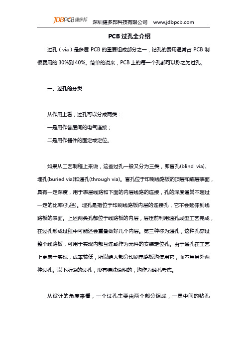
从设计的角度来看,一个过孔主要由两个部分组成,一是中间的钻孔(drill hole),二是钻孔周围的焊盘区,见下图。
这两部分的尺寸大小决定了过孔的大小。
很显然,在高速,高密度的PCB设计时,设计者总是希望过孔越小越好,这样板上可以留有更多的布线空间,此外,过孔越小,其自身的寄生电容也越小,更适合用于高速电路。
但孔尺寸的减小同时带来了成本的增加,而且过孔的尺寸不可能无限制的减小,它受到钻孔(drill)和电镀(plating)等工艺技术的限制:孔越小,钻孔需花费的时间越长,也越容易偏离中心位置;且当孔的深度超过钻孔直径的6倍时,就无法保证孔壁能均匀镀铜。
比如,现在正常的一块6层PCB板的厚度(通孔深度)为50Mil左右,所以PCB厂家能提供的钻孔直径最小只能达到8Mil。
二、过孔的寄生电容过孔本身存在着对地的寄生电容,如果已知过孔在铺地层上的隔离孔直径为D2,过孔焊盘的直径为D1,PCB板的厚度为T,板基材介电常数为ε,则过孔的寄生电容大小近似于:C=1.41εTD1/(D2-D1)过孔的寄生电容会给电路造成的主要影响是延长了信号的上升时间,降低了电路的速度。
立创 过孔规则

立创过孔规则全文共四篇示例,供读者参考第一篇示例:立创是PCB(Printed Circuit Board)的专业生产厂家,拥有多年的制造经验和技术积累。
在PCB的制造过程中,过孔是一个非常重要的环节,过孔规则的制定直接影响到PCB的质量和性能。
本文将详细介绍立创过孔规则的相关内容,希望能对读者有所帮助。
一、过孔的定义和作用在PCB中,过孔是指连接不同电路层的孔洞,通过此孔洞可以实现电路板上不同层之间的信号传输和电气连接。
过孔的作用主要有两个方面:一是连接不同电路层之间的导线,实现信号传输;二是连接电路板上的器件,实现电气连接。
过孔的质量和性能直接影响到整个PCB的质量和性能。
二、立创过孔规则的制定原则1. 符合标准和规范:立创的过孔规则要符合相关的行业标准和规范,确保PCB的质量和性能达到要求。
2. 考虑实际应用场景:过孔的设计和规格要考虑到不同的应用场景,确保PCB在各种环境下能够正常工作。
3. 兼顾成本和效率:过孔的设计和制造要兼顾成本和效率的因素,既要确保质量,又要提高生产效率。
4. 保证可靠性和稳定性:立创的过孔规则要保证过孔的可靠性和稳定性,避免因过孔质量问题导致PCB的故障。
5. 不断优化改进:立创不断优化和改进过孔规则,以适应不断变化和发展的市场需求。
立创的过孔规则包括以下几个方面的内容:1. 过孔形状和尺寸:立创的过孔形状一般采用圆形或方形,尺寸通常根据实际需求确定,包括孔径和孔间距等。
2. 过孔涂覆方式:立创采用不同的过孔涂覆方式,包括涂铜和涂锡等,确保过孔的导电性和可焊性。
3. 过孔墙厚度:立创的过孔墙厚度一般根据板厚和层数确定,保证过孔的稳定性和可靠性。
4. 过孔表面处理:立创的过孔表面一般采用化学镀铜或OSP 等处理,以提高过孔的耐腐蚀性和可焊性。
5. 过孔防焊措施:在实际制造中,立创采用不同的过孔防焊措施,避免过孔被焊料填塞,影响PCB的质量和性能。
四、结语第二篇示例:立创是PCB(Printed Circuit Board,印刷电路板)制造中一个非常重要的工艺环节。
pcb过孔工艺

pcb过孔工艺PCB(Printed Circuit Board)是印制电路板的简称,是现代电子产品制造过程中不可或缺的组成部分。
PCB的制造过程中,过孔工艺是一个非常重要的环节。
下面将从过孔的定义、过孔的分类、过孔的加工方法以及过孔的应用等方面进行介绍。
一、过孔的定义过孔是指在PCB上形成的贯穿整个板厚的通孔,用于连接不同层的电路。
通过过孔,可以实现不同层之间的电气连接,提高电路的布线密度,减小电路板的尺寸并增加电路的可靠性。
二、过孔的分类根据过孔的形状和用途,可以将过孔分为以下几种类型:1. 直通孔:直通孔是最常见的一种过孔类型,也是最基本的过孔形式。
它从PCB的一侧穿过到另一侧,用于连接电路的不同层。
2. 盲孔:盲孔是只在PCB的一侧形成的过孔,不能贯穿整个板厚。
它用于连接电路板的内层和表层。
3. 埋孔:埋孔是在PCB的内部形成的孔洞,被覆盖好后不可见。
它用于连接多层电路板内部的线路。
4. 填充孔:填充孔是在通过内层电路板时先将孔内充满导电胶或金属,然后进行制造孔。
填充孔可以提高电路板的承载能力和连接的可靠性。
三、过孔的加工方法1. 机械钻孔:机械钻孔是传统的过孔加工方法,通过机械钻头旋转和向下压力的作用,将孔钻出。
这种方法适用于大批量的生产,但钻孔精度和孔径控制较难。
2. 激光钻孔:激光钻孔是利用激光束进行钻孔的方法,具有加工速度快、孔径控制准确等优点。
激光钻孔适用于高精度的钻孔需求,但设备和操作成本较高。
3. 铣削孔:铣削孔是利用铣床进行加工的方法,通过将孔型设计在铣刀上来切削孔洞。
这种方法适用于特殊形状的过孔加工需求,但是加工速度较慢。
4. 化学铜覆盖孔:化学铜覆盖孔是一种用于盲孔的加工方法。
通过化学沉积铜,使盲孔内壁铜化,实现与其他层之间的电气连接。
四、过孔的应用PCB中的过孔广泛应用于各种电子产品的制造过程中,包括通信设备、计算机、汽车电子、工业控制等领域。
通过合理设计和制造过程控制,可以确保过孔的质量和可靠性,提高电路板的性能和使用寿命。
PCB过孔与电流计算

PCB过孔与电流计算PCB(Printed Circuit Board)过孔是指连接不同层次电路的通孔,用于传导电流、连接元件或连接电路层之间的信号。
电流计算是为了确定PCB上的过孔能够安全地承受所通过的电流。
下面将详细介绍PCB过孔的类型、工作原理以及电流计算的方法。
PCB过孔的类型主要包括通用过孔、通用布线过孔和电源过孔。
通用过孔是为了简化PCB的设计和制造过程,通常用于通过连接器引出信号。
通用布线过孔用于定义信号的起点和终点,以及通过不同信号层之间的连接。
电源过孔专门用于连接电源层,传递高电流。
PCB过孔的工作原理与普通的电路连接类似,通过导线或导轨将电流传递到需要连接的元件或电路中。
过孔的设计与制造涉及到孔径、内径、外径、层间距离等参数的确定。
通常,过孔会在PCB的设计阶段进行预先规划,并在制造过程中使用机械钻孔设备实现。
在电流计算方面,首先需要确定过孔的最大电流负载。
这需要考虑到通过过孔的电流大小以及过孔的温度上升,以保证过孔的安全运行。
电流通过过孔时会产生焦耳热,这将导致过孔的温度升高,如果温度升高过快或升高过高,过孔可能会发生熔化或损坏。
为了计算过孔的电流载荷,需要考虑以下几个因素:1.过孔的直径和长度:过孔的直径和长度决定了电流通过的截面积,较大的孔径和长度可以承载更大的电流负载。
2.过孔连接的层数:根据PCB的设计和层数,需要考虑过孔连接的层数,不同层数之间可能需要通过更多的过孔来连接。
3.PCB材料的导热性:PCB的材料和导热性能会影响过孔的温度升高速度和最终的温度。
4.过孔的环境温度:环境温度对过孔的稳定性和温度升高有一定影响。
一般来说,可以使用以下公式计算PCB过孔的最大电流负载:I=(ΔT×A×K)/R其中,I是最大电流负载,A是过孔的有效面积,ΔT是电流通过过孔时产生的温度升高,K是热传导率,R是热阻。
根据实际情况,可以选择合适的温升值,一般为10°C。
PCB过孔全介绍(PCBcrosskongfullintroduction)

PCB过孔全介绍(PCB cross kong full introduction)PCB, Kong Quan introduced.Txt3, struggle hard, the sky is still beautiful, the dream is still pure, flying self, bravely flying in the sky of dreams, I believe I must do better. 4 my bitter tears of self injury, I dream may smile. 5, cowardly people afraid of loneliness, rational people know how to enjoy solitude, this article contributed by sunli19820113DOC documents may experience poor browsing on the WAP side. It is recommended that you first select TXT, or download the source file to the local view.PCB introduced Kong Quan (via) is one of the important components of multi tier PCB, and drilling costs usually account for 30% to 40% of the cost of PCB board. In brief, each hole on the PCB can be called vias. From the point of view of function, vias can be divided into two categories: one is used as an electrical connection between the layers, and two is used as a device for fixing or positioning. If the process from the process, these vias are generally divided into three categories, namely blind hole (blind, via), via (buried) and through hole (through via). The blind hole is located on the top and bottom surface of the printed circuit board and has a depth that is used for the connection of the surface line and the inner line below. The depth of the hole usually does not exceed a certain ratio (Kong Jing). A buried hole means a connecting hole in the inner layer of a printed circuit board, which does not extend to the surface of the circuit board. The two types of holes are located in the inner layer of the circuit board, and are completed by using the through hole forming process before lamination, and may be overlapped in the process of holeformation, so as to make a few inner layers. The third is called through holes, which pass through the entire circuit board and can be used for internal interconnection or as mounting holes for components. Since vias are easier to implement and lower in cost, most printed circuit boards use it without two other vias. The vias mentioned below, without special instructions, are considered as vias. From the design point of view, an over hole is made up of two main parts, one is the middle hole (drill hole), and the other two is the pad area around the borehole. The size of these two sections determines the size of the vias. Obviously, in the high speed, high density PCB design, designers always hope through holes as small as possible, so the board can have more wiring space, in addition, a hole is small, the parasitic capacitance is smaller, more suitable for high speed circuit. But the decreasing pore size also brings cost increases, and the hole size cannot be reduced without limit, it is drilling (drill) and electroplating (plating) technology limited: the smaller the hole drilling takes longer, more easy to deviate from the center position; and when 6 times the depth of the hole over the hole diameter, hole wall can not guarantee uniform copper plating. For example, the thickness of a normal 6 piece PCB board (through hole depth) is about 50Mil, so the diameter of the drill hole provided by the PCB manufacturer is the smallest, and can only reach 8Mil. Two, the parasitic capacitance through hole vias exists on the parasitic capacitance, if the isolation hole diameter hole in the ground layer seen on D2, a hole pad diameter is D1, PCB plate thickness T, substrate dielectric constant epsilon, then the parasitic capacitance size hole similar to the C= 1.41 epsilon TD1/ (D2-D1) via the main parasitic capacitance will influence to the circuit caused by prolonged signal rise time, reduce thecircuit speed. For example, for a 50Mil plate thickness is PCB, if you use the 10Mil inner diameter, hole diameter of 20Mil pad, pad and floor area copper distance is 32Mil, the parasitic capacitance we can through the above formula calculated through hole is roughly: C= 1.41x4.4x0.050x0.020/ (0.032-0.020)=0.517pF, the the partial capacitance rise caused by time variation: T10-90=2.2C (Z0/2) =2.2x0.517x (55/2) =31.28ps. From these values we can see that,Although the effect of slow rise caused by the parasitic capacitance of a single through hole is not obvious, the designer must consider carefully if the switching between layers is used many times in the route. Three, the parasitic inductance vias, vias exist at the same time there is a parasitic capacitance and parasitic inductance, in the design of high speed digital circuit, harm parasitic inductance vias caused by parasitic capacitance is often greater than. Its parasitic series inductance will weaken the contribution of bypass capacitor and weaken the filtering effectiveness of the whole power supply system. We can use the following formula to simply calculate an over hole approximation of parasitic inductance: L=5.08h[ln (4h/d) +1], where L refers to the inductance of the through hole, h is the length of the through-hole, and D is the diameter of the center bore. It can be seen from the formula that the diameter of the through hole has little influence on the inductance, and the length of the through hole is the most influential factor on the inductance. The above example is still used to calculate the inductance of the vias: L=5.08x0.050[ln (4x0.050/0.010) +1]=1.015nH. If the signal rise time is 1ns, then the equivalent impedance is XL= PI L/T10-90=3.19 ohms. It has a high frequency current throughthe impedance can not be ignored, in particular, bypass capacitor through two holes in the connection of power and ground planes, it will increase on the parasitic inductance of hole.Through hole design through the above on the through hole parasitic characteristics analysis of four, high speed PCB, we can see that in the high-speed PCB design, seemingly simple holes will often bring a negative effect to the circuit design. In order to reduce the adverse effects caused by the parasitic effect of vias, we can do as much as possible in design: 1. From the two aspects of cost and signal quality, we should select the size of the through-hole of reasonable size. For example, the 6-10 layer memory module PCB design, the use of 10/20Mil (drilling / pad) through the hole is better, for somehigh-density small size of the board, you can also try to use the 8/18Mil through the hole. At present, it is difficult to use smaller size vias under technical conditions. For power or ground vias, a larger size may be considered to minimize impedance. 2, the two formulas discussed above can be used to reduce the two parasitic parameters of vias by using thinner PCB plates. 3, PCB signal on the board as far as possible without changing the layer, that is to say, do not use unnecessary vias. 4, the power and ground pins to the nearest hole, the hole and the pin between the shorter the better, because they will lead to an increase in inductance. At the same time, the power and ground lead should be as thick as possible to reduce the impedance. 5. Some ground vias are placed near the vias of the signal transfer layer to provide the closest loop for the signal. You can even place a number of redundant ground vias on the PCB board. Of course, flexibility is needed in design. The crosshole model discussed above is a pad for each layer, and sometimes we can reduce or even remove some layers of pads. Especially in the hole density is very large, may lead to a broken circuit partition groove is formed on a copper layer, to solve this problem in addition to move the position of the hole, we can also consider a decrease in the size of the hole pad copper layer.1. This article is contributed by sunli19820113DOC documents may experience poor browsing on the WAP side. It is recommended that you first select TXT, or download the source file to the local view.PCB introduced Kong Quan (via) is one of the important components of multi tier PCB, and drilling costs usually account for 30% to 40% of the cost of PCB board. In brief, each hole on the PCB can be called vias. From the point of view of function, vias can be divided into two categories: one is used as an electrical connection between the layers, and two is used as a device for fixing or positioning. In the process, these vias are generally classified into three groups,即盲孔(盲孔)、埋孔(埋孔)和通孔(通过)。
PCB过孔的基本概念及注意事项

PCB过孔的基本概念及注意事项PCB过孔(Via Hole)是指在PCB(Printed Circuit Board)中穿过不同层之间的电气连接,通常用于连接不同层的电路。
PCB过孔在现代电子产品中扮演着重要的角色,因此了解其基本概念和注意事项对于设计和制造高品质的PCB至关重要。
1.基本概念:PCB过孔是通过在PCB表面或内部形成的孔洞来连接不同电路层之间的电信号。
它通常由导电材料填充,在通过不同工艺加工后形成电气连接。
根据应用需要,过孔可分为三种类型:盲孔(Blind Via)、嵌孔(Buried Via)和贯通孔(Through Via)。
-盲孔:一端只链接表面层,另一端连接内部层。
-嵌孔:连接内部不同层之间,不与表面层相连。
-贯通孔:从表面直接贯通所有层,通常用于连接整个板。
2.注意事项:a.尺寸和位置:过孔的尺寸和位置对于电气连接和PCB布局至关重要。
过孔的尺寸应根据设计要求和制造工艺来确定,包括孔径、孔距、锥度等。
通过合理的过孔布局和规划,可以减少电气干涉和信号噪音。
b.信号完整性:过孔的存在会对信号传输和完整性产生影响。
高频和高速信号的传输需要更小的过孔尺寸和更好的电气连接,以减少损耗和延迟。
在设计过程中,应通过适当的仿真和测试来优化过孔的布局和参数。
c.热失真:PCB过孔在制造过程中会受到热应力的影响,因此需要防止热失真的发生。
在焊接和热浸过程中,应控制温度和加热时间以避免孔内瓷材料的破裂或导电层的剥离。
此外,过孔的周围布局应合理,以平衡板的热分布。
d.强度和可靠性:过孔的强度和可靠性对于整个PCB的性能具有重要影响。
过孔的孔壁必须光滑和均匀,以提供良好的电气性能和焊接能力。
在制造过程中,应确保过孔填充材料的粘附性和导电性,并避免孔壁的剥离和接触不良。
e.设计规则:PCB过孔的设计应符合一定的规则和标准。
必须遵守适当的PCB层内距离、过孔到电路走线的距离、过孔孔径与板厚之比等规则。
PCB过孔全介绍

孔 的 电 感 为 : L=5. 0 . 08 X 0 5 0[1 n(4 ×
孔位 于印刷线路板 的顶层和底 层表面 ,具 有一定深度 ,用于 表层线路和下面 的内层线路 的连接 ,孔 的深 度通常不超过 一 定的 比率( ) 孔是指 位于 印刷线 路板 内层 的连 接孔 , 孔径 。埋 它不会延伸到线 路板 的表面 。上述两类 孔都 位于线路板 的内 层 ,层压前利 用通孔成型 工艺完成 ,在过孔 形成过程 中可能 还会 重叠做好 几个 内层 。第 三种称 为通 孔 ,这种孔穿过 整个 线路板 ,可 用于实现 内部 互连 或作 为元 件的安装定位孔 。由 于通孔在工 艺上更易于实 现 ,成本较低 ,所以绝大部分 印刷
- 1、下载文档前请自行甄别文档内容的完整性,平台不提供额外的编辑、内容补充、找答案等附加服务。
- 2、"仅部分预览"的文档,不可在线预览部分如存在完整性等问题,可反馈申请退款(可完整预览的文档不适用该条件!)。
- 3、如文档侵犯您的权益,请联系客服反馈,我们会尽快为您处理(人工客服工作时间:9:00-18:30)。
一、PCB过孔的基础知识
过孔(via)是多层PCB的重要组成部分之一,钻孔的费用通常占PCB制板费用的30%到40%。
从过孔作用上可以分成各层间的电气连接和用作器件的固定或定位两类。
从工艺制程上来过孔一般又分为三类,即盲孔(blind via)、埋孔(buried via)和通孔(through via)。
盲孔位于印刷线路板的顶层和底层表面,具有一定深度,用于表层线路和下面的内层线路的连接,孔的深度通常不超过一定的比率(孔径)。
埋孔是指位于印刷线路板内层的连接孔,它不会延伸到线路板的表面。
上述两类孔都位于线路板的内层,层压前利用通孔成型工艺完成,在过孔形成过程中可能还会重叠做好几个内层。
第三种称为通孔,这种孔穿过整个线路板,可用于实现内部互连或作为元件的安装定位孔。
由于通孔在工艺上更易于实现,成本较低,所以绝大部分印刷电路板均使用它,而不用另外两种过孔。
从设计的角度来看,一个过孔主要由中间的钻孔(drill hole)和钻孔周围的焊盘区构成,这两部分的尺寸大小决定了过孔的大小。
过孔越小,其自身的寄生电容也越小,适合用于高速电路。
但孔尺寸的减小同时带来了成本的增加,又受到钻孔(drill)和电镀(plating)等工艺技术的限制。
二、关于过孔的寄生电容
过孔的寄生电容过孔本身存在着对寄生地的杂散电容,过孔的寄生电容会给电路造成的主要影响是延长了信号的上升时间,降低了电路的速度。
尽管单个过孔的寄生电容引起的上升延变缓的效用不是很明显,但是如果走线中多次使用过孔进行层间的切换,
设计者还是要慎重考虑的。
三、关于过孔的寄生电感
过孔存在寄生电容的同时也存在着寄生电感,在高速数字电路的设计中,过孔的寄生电感带来的危害往往大于寄生电容的影响。
它的寄生串联电感会削弱旁路电容的贡献,减弱整个电源系统的滤波效用。
过孔的直径对电感的影响较小,而对电感影响最大的是过孔的长度。
过孔产生的阻抗在有高频电流的通过已经不能够被忽略,特别要注意,旁路电容在连接电源层和地层的时候需要通过两个过孔,这样过孔的寄生电感就会成倍增加。
四、关于过孔的使用
1.从成本和信号质量两方面考虑,选择合理尺寸的过孔大小。
必要时可以考虑使用不同尺寸的过孔,比如对于电源或地线的过孔,可以考虑使用较大尺寸,以减小阻抗,而对于信号走线,则可以使用较小的过孔。
当然随着过孔尺寸减小,相应的成本也会
增加。
2.上面讨论的两个公式可以得出,使用较薄的PCB板有利于减
小过孔的两种寄生参数。
3.PCB板上的信号走线尽量不换层,也就是说尽量不要使用不
必要的过孔。
4.电源和地的管脚要就近打过孔,过孔和管脚之间的引线越短越好。
可以考虑并联打多个过孔,以减少等效电感。
5.在信号换层的过孔附近放置一些接地的过孔,以便为信号提供最近的回路。
甚至可以在PCB板上放置一些多余的接地过孔。
6.对于密度较高的高速PCB板,可以考虑使用微型过孔。