zl38003中文资料_数据手册_IC数据表
STM8S103中文资料

10 电气特性 .................................................................................................................32
10.1 参数条件............................................................................................................................32 10.1.1 最小和最大值 .............................................................................................................32 10.1.2 典型数值 ....................................................................................................................32 10.1.3 典型曲线 ....................................................................................................................32 10.1.4 负载电容 ....................................................................................................................32 10.1.5 引脚输入电压 .............................................................................................................32
XL8003降压型LED恒流驱动器芯片(高电压官方中文版)
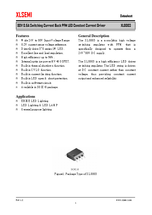
n Built in soft-start circuit.n Available in SOIC-8 package.Applicationsn EBIKE LED Lightingn LED Lighting & LED LAMPn General purpose lightingFigure1. Package Type of XL800380V 0.5A Switching Current Buck PFM LED Constant Current Driver XL8003Function BlockFigure3. Function Block Diagram of XL800380V 0.5A Switching Current Buck PFM LED Constant Current Driver XL8003 Typical application circuitFigure4. XL8003 Typical Application (3W~8W LED lamp)Ordering InformationOrder Information Marking ID Package Type Packing Type Supplied AsXL8003E1 XL8003E1 SOIC-8 2500 Units on Tape & Reel XLSEMI Pb-free products, as designated with “E1” suffix in the par number, are RoHS compliant.Absolute Maximum Ratings(Note1)Parameter Symbol Value Unit Input Voltage Vin -0.3 to 90 V Power Dissipation P D Internally limited mW Thermal Resistance (SOP-8L)R JA100 ºC/W (Junction to Ambient, No Heatsink, Free Air)Operating Junction Temperature T J-40 to 125 ºC Storage Temperature T STG-65 to 150 ºC Lead Temperature (Soldering, 10 sec) T LEAD260 ºC ESD (HBM) 3000 Vother conditions above those indicated in the operation is not implied. Exposure to absolute maximum rating conditions for extended periods may affect reliability.XL8003 Electrical CharacteristicsT a = 25℃;unless otherwise specified. Reference test circuit figure4Symbol Parameter Test Condition Min. Typ. Max. UnitVCSPCSPV oltageVIN = 24V to 80V,Iled=0.3A, Pout=8W190 200 210 mVEfficiency ŋVIN=48V, Iled=0.3A, Pout=8W - 94.78 - % Efficiency ŋVIN=60V, Iled=0.3A, Pout=8W - 93.99 - % Efficiency ŋVIN=72V, Iled=0.3A, Pout=8W - 92.55 - %Electrical Characteristics (DC Parameters)Parameters Symbol Test Condition Min. Typ. Max. Unit Input operation voltage VIN 24 80 VSwitching Frequency Fosc Figure4 (8*1W)VIN=48V53.8 67.2 80.6 KHzSwitching Frequency Fosc Figure4 (8*1W)VIN=60V64.2 80.2 96.2 KHzSwitching Frequency Fosc Figure4 (8*1W)VIN=72V70.0 87.4 104.8 KHzOutput LED open voltage V open Figure4 VIN=72V 36 VDMOS Drain-SourceBreakdown V oltageV BRDS V GS=0V, I DS=250uA 90 V DMOSDrain-Source on resistorR DSON I DS=0.5A, V GS=10V 0.1 0.15 Ohm Thermal Shutdown OTP Tj 165 0C Thermal Shutdown Window 25 0C80V 0.5A Switching Current Buck PFM LED Constant Current Driver XL8003 [1] Typical application circuit (3W ~ 8W)Figure5. XL8003 System Application (3W ~ 8W)The figure5 system parameters as following:VIN=36V DC1W LED Series Vin(V) Iin(mA) Vout(V) Iout(mA) Fosc(KHz) Effiency(%)3 35.97 89 9.60 297 44.9 89.064 35.98 114 12.79 294 50.0 91.685 35.98 140 16.07 291 53.7 92.846 35.97 164 19.22 289 53.0 94.167 35.96 188 22.41 287 49.1 95.148 35.96 212 25.68 285 41.8 96.00VIN=48V DC1W LED Series Vin(V) Iin(mA) Vout(V) Iout(mA) Fosc(KHz) Effiency(%)3 47.99 68 9.62 300 47.6 88.444 47.99 87 12.79 298 56.2 91.295 47.99 107 16.07 295 62.6 92.326 47.98 125 19.21 292 66.6 93.537 47.98 144 22.41 290 68.1 94.068 47.98 162 25.67 287 67.2 94.78Figure6. XL8003 System efficiency curvePackage InformationSOP8 Package Mechanical Dimensions。
zl38010中文资料_数据手册_IC数据表

1Features•Full duplex transcoder with four encode channels and four decode channels•32kbps, 24kbps and 16kbps ADPCM coding complying with ITU-T (previously CCITT) G.726 (without 40kbps), and ANSI T1.303-1989•Low power operation, 6.5mW typical•Asynchronous 4.096MHz master clock operation •SSI and ST-BUS interface options •Transparent PCM bypass •Transparent ADPCM bypass •Linear PCM code•No microprocessor control required •Simple interface to Codec devices •Pin selectable µ−Law or A-Law operation •Pin selectable ITU-T or signed magnitude PCM coding•Single 3.3Volts power supplyApplications•Pair gain•Voice mail systems•Wireless telephony systemsDescriptionThe Quad ADPCM Transcoder is a low power, CMOS device capable of four encode and four decode functions per frame. Four 64kbps PCM octets are compressed into four 32, 24 or 16kbps ADPCM words,and four 32, 24 or 16 kbps ADPCM words are expanded into four 64kbps PCM octets. The 32, 24and 16kbps ADPCM transcoding algorithms utilized conform to ITU-T Recommendation G.726 (excluding 40kbps), and ANSI T1.303 - 1989.January 2007Ordering InformationZL38010DCE 28 Pin SOIC TubesZL38010DCF 28 Pin SOIC Tape & Reel ZL38010DCE128 Pin SOIC**TubesZL38010DCF128 Pin SOIC**Tape & Reel**Pb Free Matte Tin-40°C to +85°CZL38010Low Power Quad ADPCM TranscoderData SheetFigure 1 - Functional Block DiagramADPCM I/OPCM I/OControl DecodeVDD VSS PWRDN IC MS1MS2A/µFORMAT MS5MS4MS3MS6LINEAR SELTimingADPCMi ADPCMoENB1ENB2/F0odBCLK F0i MCLK C2o EN1EN2PCMo1PCMi1PCMo2PCMi2Full Duplex Quad TranscoderZL38010Data SheetSwitching, on-the-fly, between 32kbps and 24kbps ADPCM, is possible by controlling the appropriate mode select (MS1 - MS6) control pins. All optional functions of the device are pin selectable allowing a simple interface to industry standard codecs, digital phone devices and Layer 1 transceivers. Linear coded PCM is provided to facilitate external DSP functions.Change SummaryChanges from October 2005 Issue to January 2007 Issue.Figure 2 - Pin ConnectionsPin Description Page ItemChange1Ordering Information BoxAdded Pb Free part numbers.Pin #Name Description1EN1Enable Strobe 1 (Output). This 8 bit wide, active high strobe is active during the B1 PCM channel in ST-BUS mode. Becomes a single bit, high true pulse when LINEAR=1. In SSI mode this output is high impedance.2MCLKMaster Clock (input). This is a 4.096MHz (minimum) input clock utilized by thetranscoder function; it must be supplied in both ST-BUS and SSI modes of operation. In ST-BUS mode the C4 ST-BUS clock is applied to this pin. This synchronous clock is also used to control the data I/O flow on the PCM and ADPCM input/output pins according to ST-BUS requirements.In SSI mode this master clock input is derived from an external source and may beasynchronous with respect to the 8kHz frame. MCLK rates greater than 4.096MHz are acceptable in this mode since the data I/O rate is governed by BCLK.3F0i Frame Pulse (Input). Frame synchronization pulse input for ST-BUS operation. SSI operation is enabled by connecting this pin to V SS .4C2o2.048MHz Clock (Output). This ST-BUS mode bit clock output is the MCLK (C4) input divided by two, inverted, and synchronized to F0i. This output is high-impedance during SSI operation.12345678910111213141516171819202827262524232221MS1VDD MS3ICMS4FORMAT MS2PWRDN ADPCMi ADPCMo MS5MS6EN2PCMo1BCLK PCMi1LINEAR ENB2/F0odVSS C2o MCLK F0i PCMi2ENB1PCMo2EN1SEL A/µZL38010Data SheetPin #Name Description5BCLK Bit Clock (Input). 128kHz to 4096kHz bit clock input for both PCM and ADPCM ports;used in SSI mode only. The falling edge of this clock latches data into ADPCMi, PCMi1and PCMi2. The rising edge clocks data out on ADPCMo, PCMo1 and PCMo2. This inputmust be tied to V SS for ST-BUS operation.6PCMo1Serial PCM Stream 1 (Output). 128kbps to 4096kbps serial companded/linear PCM out-put stream. Data are clocked out by rising edge of BCLK in SSI mode. Clocked out byMCLK divided by two in ST-BUS mode. See Figure 14.7PCMi1Serial PCM Stream 1 (Input). 128kbps to 4096kbps serial companded/linear PCM input stream. Data are clocked in on falling edge of BCLK in SSI mode. Clocked in at the3/4 bit position of MCLK in ST-BUS mode. See Figure 14.8V SS Digital Ground. Nominally 0 volts9LINEAR Linear PCM Select (Input). When tied to V DD the PCM I/O ports (PCM1,PCM2) are 16-bit linear PCM. Linear PCM operates only at a bit rate of 2048kbps. Companded PCM isselected when this pin is tied to V SS. See Figure 5 & Figure 8.10ENB2/F0od PCM B-Channel Enable Strobe 2 (Input) / Delayed Frame Pulse (Output).SSI operation: ENB2 (Input). An 8-bit wide enable strobe input defining B2 channel(AD)PCM data. A valid 8-bit strobe must be present at this input for SSI operation. SeeFigure 4 & Figure 6.ST-BUS operation: F0od(Output). This pin is a delayed frame strobe output. When LIN-EAR=0, this becomes a delayed frame pulse output occurring 64 C4 clock cycles afterF0i and when LINEAR = 1 at 128 C4 clock cycles after F0i. See Figures 7, 8, 9 & 14.11ENB1PCM B-Channel Enable Strobe 1 (Input).SSI operation: An 8-bit wide enable strobe input defining B1 channel (AD)PCM data. Avalid 8-bit strobe must be present at this input for SSI operation.ST-BUS operation: When tied to V SS transparent bypass of the ST-BUS D- and C- chan-nels is enabled. When tied to V DD the ST-BUS D-channel and C-channel output timeslotsare forced to a high-impedance state.12PCMo2Serial PCM Stream 2 (Output). 128kbps to 4096kbps serial companded/linear PCM out-put stream. Clocked out by rising edge of BCLK in SSI mode. Clocked out by MCLK divid-ed by two in ST-BUS mode. See Figure 14.13PCMi2Serial PCM Stream 2 (Input). 128kbps to 4096kbps serial companded/linear PCM input stream. Data bits are clocked in on falling edge of BCLK in SSI mode. Clocked in at the3/4 bit position of MCLK in ST-BUS mode. See Figure 14.14SEL SELECT (Input).PCM bypass mode: When SEL=0 the PCM1 port is selected for PCM bypass operationand when SEL=1 the PCM2 port is selected for PCM bypass operation.See Figure 6 & Figure 9.16kbps transcoding mode:SSI Operation - in 16kbps transcoding mode, the ADPCM words are assigned to the I/Otimeslot defined by ENB2 when SEL=1 and by ENB1 when SEL=0. See Figure 4.ST-BUS operation- in 16kbps transcoding mode, the ADPCM words are assigned to theB2 timeslot when SEL=1 and to the B1 timeslot when SEL=0. See Figure 9.ZL38010Data SheetAll unused inputs should be connected to logic low or high unless otherwise stated. All outputs should be left open circuit when not used.All inputs have TTL compatible logic levels except for MCLK which has CMOS compatible logic levels and PWRDN which has Schmitt trigger compatible logic levels.All outputs are CMOS with CMOS logic levels (See DC Electrical Characteristics).15A/µA-Law/µ−Law Select (Input). This input pin selects µ−Law companding when set to logic 0, and A-Law companding when set to logic 1. This control is for all channels.This input is ignored in Linear mode during which it may be tied to V SS or V DD .16FORMATFORMAT Select (Input). Selects ITU-T PCM coding when high and Sign-Magnitude PCM coding when low. This control is for all channels.This input is ignored in Linear mode during which it may be tied to V SS or V DD .17PWRDN Power-down (Input). An active low reset forcing the device into a low power mode where all outputs are high-impedance and device operation is halted. 18IC Internal Connection (Input). Tie to V SS for normal operation.192021MS1MS2MS3Mode Selects 1, 2 and 3 (Inputs). Mode selects for all four encoders.MS3MS2MS1MODE 00032kbps ADPCM 00124kbps ADPCM 01016kbps ADPCM in EN1/ENB1 when SEL=0in EN2/ENB2 when SEL=1011ADPCM Bypass for 32kbps and 24kbps 100ADPCM Bypass for 16kbps 101PCM Bypass (64kbps) to PCM1 if SEL=0, PCM2 if SEL=1110Algorithm reset (ITU-T optional reset)111ADPCMo disable 22V DD Positive Power Supply. Nominally 3.3Volts +/-10%23ADPCMiSerial ADPCM Stream (Input). 128kbps to 4096kbps serial ADPCM word input stream. Data bits are clocked in on falling edge of BCLK in SSI mode and clocked in on the 3/4 bit edge of MCLK in ST-BUS mode.24ADPCMoSerial ADPCM Stream (Output). 128kbps to 4096kbps serial ADPCM word output stream. Data bits are clocked out by rising edge of BCLK in SSI mode and clocked out by MCLK divided by two in ST-BUS mode.252627MS4MS5MS6Mode Selects 4, 5 and 6 (Inputs). Mode selects for all four decoders.MS6MS5MS4MODE 00032kbps ADPCM 00124kbps ADPCM 01016kbps ADPCM in EN1/ENB1 when SEL=0in EN2/ENB2 when SEL=1011ADPCM Bypass for 32kbps and 24kbps 100ADPCM Bypass for 16kbps 101PCM Bypass (64kbps) to PCM1 if SEL=0, PCM2 if SEL=1110Algorithm reset (ITU-T optional reset)111PCMo1/2 disable 28EN2Enable Strobe 2 (Output). This 8 bit wide, active high strobe is active during the B2 PCM channel in ST-BUS mode. Forced to high impedance when LINEAR=1.Pin #Name DescriptionZL38010Data Sheet Functional DescriptionThe Quad-channel ADPCM Transcoder is a low power, CMOS device capable of four encode and four decode operations per frame. Four 64kbps channels (PCM octets) are compressed into four 32, 24 or 16kbps ADPCM channels (ADPCM words), and four 32, 24 or 16kbps ADPCM channels (ADPCM words) are expanded into four 64kbps PCM channels (PCM octets). The ADPCM transcoding algorithm utilized conforms to ITU-T recommendation G.726 (excluding 40kbps), and ANSI T1.303 - 1989. Switching on-the-fly between 32 and 24kbps transcoding is possible by toggling the appropriate mode select pins (supports T1 robbed-bit signalling). All functions supported by the device are pin selectable. The four encode functions comprise a common group controlled via Mode Select pins MS1, MS2 and MS3. Similarly, the four decode functions form a second group commonly controlled via Mode Select pins MS4, MS5 and MS6. All other pin controls are common to the entire transcoder.The device requires 6.5mWatts (MCLK= 4.096MHz) typically for four channel transcode operation. A minimum master clock frequency of 4.096MHz is required for the circuit to complete four encode channels and four decode channels per frame. For SSI operation a master clock frequency greater than 4.096MHz and asynchronous, relative to the 8kHz frame, is allowed.The PCM and ADPCM serial busses support both ST-BUS and Synchronous Serial Interface (SSI) operation. This allows serial data clock rates from 128kHz to 4096kHz, as well as compatibility with Zarlink’s standard Serial Telecom BUS (ST-BUS). For ST-BUS operation, on chip channel counters provide channel enable outputs as well as a 2048kHz bit clock output which may be used by down-stream devices utilizing the SSI bus interface.Linear coded PCM is also supported. In this mode the encoders compress, four 14-bit, two’s complement (S,S,S,12,...,1,0), uniform PCM channels into four 4, 3 or 2 bit ADPCM channels. Similarly, the decoder expands four 4, 3 or 2 bit ADPCM channels into four 16-bit, two’s complement (S,14,...,1,0), uniform PCM channels. The data rate for both ST-BUS and SSI operation in this mode is 2048 kbps.ZL38010Data Sheet Serial (AD)PCM Data I/OSerial data transfer to/from the Quad ADPCM transcoder is provided through one ADPCM and two PCM ports (ADPCMi, ADPCMo, PCMi1, PCMo1, PCMi2, PCMo2). Data is transferred through these ports according to either ST-BUS or SSI requirements. The device determines the mode of operation by monitoring the signal applied to the F0i pin. When a valid ST-BUS frame pulse (244nSec low going pulse) is applied to the F0i pin the transcoder will assume ST-BUS operation. If F0i is tied continuously to V SS the transcoder will assume SSI operation. Pin functionality in each of these modes is described in the following sub-sections.ST-BUS ModeDuring ST-BUS operation the C2o, EN1, EN2 and F0od outputs become active and all serial timing is derived from the MCLK (C4) and F0i inputs while the BCLK input is tied to V SS. (See Figures 7, 8 & 9.)Basic Rate “D” and “C” ChannelsIn ST-BUS mode, when ENB1 is brought low, transparent transport of the ST-BUS "Basic Rate D- and C-channels" is supported through the PCMi1 and PCMo1 pins. This allows a microprocessor controlled device, connected to the PCMi/o1 pins, to access the "D" and "C" channels of a transmission device connected to the ADPCMi/o pins. When ENB1 is brought high, the “D” and “C” channel outputs are tristated. Basic Rate “D” and “C” channels are not supported in LINEAR mode.(See Figure 7.)SSI ModeDuring SSI operation the BCLK, ENB1 and ENB2/F0od inputs become active. The C2o, EN1, and EN2 outputs are forced to a high-impedance state except during LINEAR operation during which the EN1 output remains active. (See Figures 4, 5 & 6.)The SSI port is a serial data interface, including data input and data output pins, a variable rate bit clock input and two input strobes providing enables for data transfers. There are three SSI I/O ports on the Quad ADPCM; the PCMi/o1 PCM port, the PCMi/o2 PCM port, and the ADPCMi/o port. The two PCM ports may transport 8-bit companded PCM or 16-bit linear PCM. The alignment of the channels is determined by the two input strobe signals ENB1 and ENB2/F0od. The bit clock (BCLK) and input strobes (ENB1 and ENB2/F0od) are common for all three of the serial I/O ports. BCLK can be any frequency between 128kHz and 4096kHz synchronized to the input strobes. BCLK may be discontinuous outside of the strobe boundaries except when LINEAR=1. In LINEAR mode, BCLK must be 2048kHz and continuous for 64 cycles after the ENB1 rising edge and for the duration of ENB2/F0od. Mode Select Operation (MS1, MS2, MS3, MS4, MS5, MS6)Mode Select pins MS1, MS2 and MS3 program different bit rate ADPCM coding, bypass, algorithmic reset and disable modes for all four encoder functions simultaneously. When 24kbps ADPCM mode is selected bit 4 is unused while in 16kbps ADPCM mode all ADPCM channels are packed contiguously into one 8-bit octet. Mode Select pins MS4, MS5 and MS6 operate in the same manner for the four decode functions. The mode selects must be set up according to the timing constraints illustrated in Figures 16 and 17.32 kbps ADPCM ModeIn 32kbps ADPCM mode, the 8-bit PCM octets of the B1, B2, B3 and B4 channels (PCMi1 and PCMi2) are compressed into four 4-bit ADPCM words on ADPCMo. Conversely, the 4-bit ADPCM words of the B1, B2, B3 and B4 channels from ADPCMi are expanded into four 8-bit PCM octets on PCMo1 and PCMo2. The 8-bit PCM octets (A-Law or µ-Law) are transferred most significant bit first starting with b7 and ending with b0. ADPCM words are transferred most significant bit first starting with I1 and ending with I4 (See Figures 4 & 7). Reference ITU-T G.726 for I-bit definitions.ZL38010Data Sheet24 kbps ADPCM ModeIn 24kbps mode PCM octets are transcoded into 3-bit words rather than the 4-bit words utilized in 32kbps ADPCM. This is useful in situations where lower bandwidth transmission is required. Dynamic operation of the mode select control pins will allow switching from 32kbps mode to 24kbps mode on a frame by frame basis. The 8 bit PCM octets (A-Law or µ-Law) are transferred most significant bit first starting with b7 and ending with b0. ADPCM words are transferred most significant bit first starting with I1 and ending with I3 (I4 becomes don’t care). (See Figures 4 & 7.)16 kbps ADPCM ModeWhen SEL is set to 0, the 8-bit PCM octets of the B1, B2, B3 and B4 channels (PCMi1 and PCMi2) are compressed into four 2-bit ADPCM words on ADPCMo during the ENB1 timeslot in SSI mode and during the B1 timeslot in ST-BUS mode. Similarly, the four 2-bit ADPCM words on ADPCMi are expanded into four 8-bit PCM octets (on PCMo1 and PCMo2) during the ENB1/B1 timeslot. (See Figures 4 & 7.)When SEL is set to 1, The same conversion takes place as described when SEL = 0 except that the ENB2/B2 timeslots are utilized.A-Law or µ-Law 8-bit PCM are received and transmitted most significant bit first starting with b7 and ending with b0. ADPCM data are most significant bit first starting with I1 and ending with I2.ADPCM BYPASS (32 and 24 kbps)In ADPCM bypass mode the B1 and B2 channel ADPCM words are bypassed (with a two-frame delay) to/from the ADPCM port and placed into the most significant nibbles of the PCM1/2 port octets. Note that the SEL pin performs no function for these two modes (See Figures 6 & 9). LINEAR, FORMAT and A/µ pins are ignored in bypass mode. In 32kbps ADPCM bypass mode, Bits 1 to 4 of the B1, B2, B3 and B4 channels from PCMi1 and PCMi2 are transparently passed, with a two frame delay, to the same channels on ADPCMo. In the same manner, the B1, B2, B3 and B4 channels from ADPCMi are transparently passed, with a two frame delay, to the same channels on PCMo1 and PCMo2 pins. Bits 5 to 8 are don’t care. This feature allows two voice terminals, which utilize ADPCM transcoding, to communicate through a system without incurring unnecessary transcode conversions. This arrangement allows byte-wide or nibble-wide transport through a switching matrix.24kbps ADPCM bypass mode is the same as 32 kbps mode bypass excepting that only bits 1 to 3 are bypassed and bits 4 to 8 are don’t care.ADPCM BYPASS (16 kbps)When SEL is set to 0, only bits 1 and 2 of the B1, B2, B3 and B4 PCM octets (on PCMi1 and PCMi2) are bypassed, with a two frame delay, to the same channels on ADPCMo during the ENB1 timeslot in SSI mode and during the B1 timeslot in ST-BUS mode. Similarly, the four 2-bit ADPCM words on ADPCMi are transparently bypassed, with a two frame delay, to PCMo1 and PCMo2 during the ENB1 or B1 timeslot. Bits 3-8 are don’t care. (See Figures 6 & 9.)When SEL is set to 1, the same bypass occurs as described when SEL = 0 except that the ENB2 or B2 timeslots are utilized.LINEAR, FORMAT and A/µ pins are ignored in bypass mode.ZL38010Data SheetPCM BYPASSWhen SEL is set to 0, the B1 and B2 PCM channels on PCMi1 are transparently passed, with a two-frame delay, to the same channels on the ADPCMo. Summarily, the two 8-bit words which are on ADPCMi are transparently passed, with a two-frame delay, to channels B1 and B2 of PCMo1 while PCMo2 is set to a high-impedance state.(See Figures 6 & 9.)When SEL is set to 1, the B3 and B4 channels on PCMi2 are transparently passed, with a two frame delay, to the same channels on ADPCMo. Similarly, the two 8-bit words which are on ADPCMi are transparently passed, with a two-frame delay, to channels B3 and B4 of PCMo2. In this case PCMo1 is always high-impedance if ENB1 = 0. If ENB1 = 1 during ST-BUS operation then the D and C channels are active on PCMo1.LINEAR, FORMAT and A/µ pins are ignored in bypass mode.Algorithm Reset ModeWhile an algorithmic reset is asserted the device will incrementally converge its internal variables to the 'Optional reset values' stated in G.726. Algorithmic reset requires that the master clock (MCLK) and frame pulse (ENB1/2 or F0i) remain active and that the reset condition be valid for at least four frames. Note that this is not a power down mode; see PWRDN for this function.ADPCMo & PCMo1/2 DisableWhen the encoders are programmed for ADPCMo disable (MS1 to MS3 set to 1) the ADPCMo output is set to a high impedance state and the internal encode function remains active. Therefore convergence is maintained. The decode processing function and data I/O remain active.When the decoders are programmed for PCMo1/2 disable (MS4 to MS6 set to 1) the PCMo1/2 outputs are high impedance during the B Channel timeslots and also, during ST-BUS operation, the D and C channel timeslots according to the state of ENB1. Therefore convergence is maintained. The encode processing function and data I/O remain active.Whenever any combination of the encoders or decoders are set to the disable mode the following outputs remain active. A) ST-BUS mode: ENB2/F0od, EN1, EN2 and C2o. Also the “D” and “C” channels from PCMo1 and ADPCMo remain active if ENB1 is set to 0. If ENB1 is brought high then PCMo1 and ADPCMo are fully tri-stated. B) SSI mode: When used in the 16-bit linear mode, only the EN1 output remains active. For complete chip power down see PWRDN.ZL38010Data Sheet Other Pin Controls16 Bit Linear PCMSetting the LINEAR pin to logic one causes the device to change to 16-bit linear (uniform) PCM transmission on the PCMi/o1 and PCMi/o2 ports. The data rate for both ST-BUS and SSI operation in this mode is 2048 kbps and all decode and encode functions are affected by this pin. In SSI mode, the input channel strobes ENB1 and ENB2/F0od remain active for 8 cycles of BCLK for an ADPCM transfer. The EN1 output is high for one BCLK period at the end of the frame (i.e., during the 256th BCLK period). In ST-BUS mode, the output strobes EN1 and ENB2/F0od are adjusted to accommodate the required PCM I/O streams. The EN1 output becomes a single bit high true pulse during the last clock period of the frame (i.e., the 256th bit period) while ENB2/F0od becomes a delayed, low true frame-pulse (F0od) output occurring during the 64th bit period after the EN1 rising edge.Linear PCM on PCMi1 and PCMi2, are received as 14-bit, two’s complement data with three bits of sign extension in the most significant positions (i.e., S,S,S,12,...1,0) for a total of 16 bits. The linear PCM data transmitted from PCMo1 and PCmo2 are 16-bit, two’s complement data with one sign bit in the most significant position (i.e., S,14,13,...1,0)32 and 24 kbps ADPCM modeIn 32kbps and 24kbps linear mode, the 16-bit uniform PCM dual-octets of the B1, B2, B3 and B4 channels (from PCMi1 and PCMi2) are compressed into four 4-bit words on ADPCMo. The four 4-bit ADPCM words of the B1, B2, B3 and B4 channels from ADPCMi are expanded into four 16-bit uniform PCM dual-octets on PCMo1 and PCMo2. 16-bit uniform PCM are received and transmitted most significant bit first starting with b15 and ending with b0. ADPCM data are transferred most significant bit first starting with I1 and ending with I4 for 32kbps and ending with I3 for 24kbps operation (i.e., I4 is don’t care).(See Figures 5 & 8.)16 kbps ADPCM modeWhen SEL is set to 0, the four, 2-bit ADPCM words are transmitted/received on ADPCMo/i during the ENB1 time-slot in SSI mode and during the B1 timeslot in ST-BUS mode. When SEL is set to 1, the four, 2-bit ADPCM words are transmitted/received on ADPCMo/i during the ENB2 timeslot in SSI mode and during the B2 timeslot in ST-BUS mode. (See Figures 5 & 8.)PCM Law Control (A/µ, FORMAT)The PCM companding/coding law invoked by the transcoder is controlled via the A/µ and FORMAT pins. ITU-T G.711 companding curves, µ-Law and A-Law, are selected by the A/µ pin (0=µ-Law; 1=A-Law). Per sample, digital code assignment can conform to ITU-T G.711 (when FORMAT=1) or to Sign-Magnitude coding (when FORMAT=0). Table 1 illustrates these choices.ZL38010Data SheetTable 1 - Companded PCMPower DownSetting the PWRDN pin low will asynchronously cause all internal operation to halt and the device to go to a power down condition where no internal clocks are running. Output pins C2o, EN1, EN2, PCMo1, PCMo2 and ADPCMo and I/O pin F0od/ENB2 are forced to a high-impedance state. Following the reset (i.e., PWRDN pin brought high)and assuming that clocks are applied to the MCLK and BCLK pins, the internal clocks will still not begin to operate until the first frame alignment is detected on the ENB1 pin for SSI mode or on the F0i pin for ST-BUS mode. The C2o clock and EN1, EN2 pins will not start operation until a valid frame pulse is applied to the F0i pin. If the F0i pin remains low for longer than 2 cycles of MCLK then the C2o pin will top toggling and will stay low. If the F0i pin is held high then the C2o pin will continue to operate. In ST-BUS mode the EN1 and EN2 pins will stop toggling if the frame pulse (F0i) is not applied every frame.Master Clock (MCLK)A minimum 4096kHz master clock is required for execution of the transcoding algorithm. The algorithm requires 512 cycles of MCLK during one frame for proper operation. For SSI operation this input, at the MCLK pin, may be asynchronous with the 8kHz frame provided that the lowest frequency and deviation due to clock jitter still meets the strobe period requirement of a minimum of 512 t C4P - 25%t C4P (see Figure 3). For example, a system producing large jitter values can be accommodated by running an over-speed MCLK that will ensure a minimum 512 MCLK cycles per frame is obtained. The minimum MCLK period is 61nSec, which translates to a maximum frequency of 16.384MHz. Extra MCLK cycles (>512/frame) are acceptable since the transcoder is aligned by the appropriate strobe signals each frame.Figure 3 - MCLK Minimum RequirementFORMAT01PCM CodeSign-Magnitude A/µ = 0 or 1ITU-T (G.711)(A/µ = 0)(A/µ = 1)+ Full Scale 1111 11111000 00001010 1010+ Zero 1000 00001111 11111101 0101- Zero 0000 00000111 11110101 0101- Full Scale0111 11110000 00000010 1010ENB1MCLK512 t C4P - 25%t C4P MinimumZL38010Data Sheet Bit Clock (BCLK)For SSI operation the bit rate, for both ADPCM and PCM ports, is determined by the clock input at BCLK. BCLK must be eight periods in duration and synchronous with the 8kHz frame inputs at ENB1 and ENB2. Data is sampled at PCMi1/2 and at ADPCMi concurrent with the falling edge of BCLK. Data is available at PCMo1/2 and ADPCMo concurrent with the rising edge of BCLK. BCLK may be any rate between 128kHz and 4096kHz. For ST-BUS operation BCLK is ignored (tie to V SS) and the bit rate is internally set to 2048kbps.Figure 4 - SSI 8-Bit Companded PCM Relative TimingZL38010Data SheetFigure 5 - SSI 16-Bit Linear PCM Relative TimingZL38010Data SheetFigure 6 - SSI PCM and ADPCM Bypass Relative TimingZL38010Data SheetFigure 7 - ST-BUS 8-Bit Companded PCM Relative TimingZL38010Data SheetFigure 8 - ST-BUS 16-Bit Linear PCM Relative TimingZL38010Data SheetFigure 9 - ST-BUS PCM and ADPCM Bypass Relative TimingZL38010Data Sheet Processing Delay Through the DeviceIn order to accommodate variable rate PCM and ADPCM interfaces, the serial input and output streams require a complete frame to load internal shift registers. Internal frame alignment of the encoding/decoding functions are taken from either of the F0i or ENB1 & ENB2 input strobes depending upon the device operating mode (i.e., ST-BUS or SSI). The encoding/decoding of all channels then takes one frame to complete before the output buffers are loaded. This results in a two frame transcoding delay. The two frame delay also applies to the D and C channels and to the PCM and ADPCM bypass functions.(See Figure 10.)Note: When changing the relative positions of the ENB1 and ENB2 strobes, precaution must be taken to ensure that two conditions are met. They are:1.There must be at least 512 master clock cycles between consecutive rising edges of ENB1. This condition alsoholds true for ENB2.2.The ENB1 strobe must alternate with the ENB2 strobe.Violation of these requirements may cause noise on the output channels.Figure 10 - Data ThroughputApplicationsFigure 11 depicts an ISDN line card utilizing a ’U’ interface transceiver and ZL38010 ADPCM transcoder. This central office application implements the network end of a Pair-Gain system. Figure 12 shows Zarlink devices used to construct the remote Pair-Gain loop terminator.。
3W3中文手册(通用)

U n i n t e r r u p t i b l eP o w e r S u p p l y用户手册U S E R′S M A N U A L10-40KVA三相输出Three-phase Outputpag. 2 / 29安全规范注意事项本手册包含安装与操作本产品的说明.。
请在安装前由经过专业训练的人员详细阅读本手册。
因为本手册包含基本的使用说明。
请妥善保存!安全规范■ 本产品安装时必须接地请确保地线牢固地索附在有右图标示的接地铜条上:■ 所有关于本产品内部的维修保养工作必须由经过专业训练的人员操作■ 在需要更换保险丝的情形时,请更换同样型式与规格的保险丝(请参阅”设置输出入配线”章节). ■ 在必须切断UPS 的输入市电时,请断开前面板内的所有开关,或者经由UPS 的控制面板选择”SYSTEM OFF”电瓶更换必须由专业人员执行.更换之后的废电瓶请交由专业的废电的处置,因为电池内 可能有对环境造成污染的物质!由于本产品不断的改良与研发,对于本手册内容有所修正时将不另行通知.欢迎您随时与我们联系以取得最新信息.电磁干扰要求本产品”不断电式电源供应器”(UPS),符合基本的电磁干扰要求:EMC 指令89/336e 92/31 a 93/68 ECC.使用说明警告:本产品属于A 等级的UPS.在居住的环境中,本产品可能会造成无线电干扰,此情况下,使用者可能必须采取适当的措施.例如:当电视或者收音机受到干扰时,可将本产品搬移到适当的距离以减少干扰情形.索引外观位置图 (5)储存 (5)安装环境 (6)前置作业 (6)安装环境 (6)安装位置 (6)设置输出入配线 (7)保护 (7)UPS内部 (7)UPS输入 (7)UPS 输出,短路与选择性 (7)差异 (8)配线与连接 (8)启动UPS前置作业 (8)市电与负载连接 (9)三相输出(输入:三相) (9)电瓶 (9)外接电瓶箱 (9)内接电瓶箱 (9)连接状况 (9)开机程序 (9)功能检查 (10)关机 (10)配置模式 (10)在线式(ON - LINE) (10)待机经济模式(STANDBY-ON operation) (10)操作模式 (11)电瓶操作模式(不属于稳压器配置模式) (11)旁路操作模式 (12)手动旁路维护模式 (12)维护 (13)UPS 部件 (13)输入 / 输出过滤器 (13)转换器 (13)pag. 3 / 29逆变器 (14)旁路 (14)SWMB (手动维护开关), SWIN, SWOUT (14)电瓶 (14)RS232 n.1 与 n. 2 介面 (14)讯号及指令面板 (14)EPO连接器 (15)规格 (16)系统 (16)转换器输入 (16)转换器输出 (17)电瓶 (17)输出逆变器 (17)旁路 (17)状态讯息显示 (18)概述 (18)警示灯号: LED (18)警告讯息 (19)控制面板 (20)基本选单 (20)Key menu 1, "?", HELP (20)Key menu 2 "测量" (20)Key menu 2, 2 : “输出测量” (21)Key menu 3 "KEY", 指令 (21)Key menu 3, 2: 电瓶测试 (21)Key menu 3, 5: 使用者自订 (22)Key menu 3, 5, 436215, 2: 工作模式和功率设定 (22)Key menu 3, 5, 436215,3:输出电压,旁路电压范围,旁路频率范围的设定 (22)Key menu 3, 5, 436215, 4:电池数量,电池浮充电压,电池容量设定 (22)Key menu 3, 5, 436215,5:电池定时自测试设定 (22)Key menu 3, 6: 逆变器关闭 / 切至旁路模式 (23)Key menu 3, 7: 系统完全关机设定 (23)Key menu 4:事件记录 (23)故障代码表 (25)附录 (27)尺寸 / 重量 (28)pag. 4 / 29pag. 5 / 29外观位置图1. 控制面板2. 上面板3. 前面板4. 滑轮5. 背面通风孔6. 散热孔7. 风扇网格 8. EPO 连接器9. REMOTE 连接器 10. RS232-2 通讯端口 11. RS232-1 通讯端口 12. 侧面板储存本产品的储存条件如下:温 度:0°- 40°C (32°- 104°F) 相对湿度:< 95%UPS 内含电瓶时:UPS 内部的电瓶会因为化学变化而自我放电.假如您并非要立即使用本产品,请注意外装箱上标示的再充电日期(此标示只有在UPS 内含电瓶时才会有),并在期限内再充电!再充电只要提供UPS输入电源并开机限内再充电,保持在”正常模式”下运作至少24小时安装环境三相输出额定容量 [kVA] 10 15 20 30 40 操作温度0 ± 40 °C最大相对湿度95 % (无冷凝)最大操作高度4000m尺寸 (长 x 宽 x 高) [mm] 505 x 720 x 1140 505 x825 x 1215 UPS 重量100 114 120 126 140在标称负载及电瓶充电时的能量损失.[kW / kcal /B.T.U.]0.760024001.0490036001.39120048002.1180071002.824009600允许通过的空气流速(室内装置)[立方公尺/小时] 370 557 742 1100 1400 最大漏电流 (mA) < 100 mA保护等级IP20配线箱体底部前置作业本产品出厂时附有:- 保证书- 使用手册·-Nr. 3输入电瓶保险丝,-Nr. 2 输入电瓶箱保险丝(假如内接电瓶存在时)安装环境· 避免灰尘量太大,或者空气内有其它粉尘类的物质.· 确认安装的地板可以承受UPS以及电瓶箱的重量(请参照”尺寸与重量”章节) · 请检查安装的地点有足够的空间,不会造成日后维修的困扰· UPS操作时的环境必须在0-40℃之间.本产品可以在0-40℃之间正常操作.建议最佳的UPS与电瓶操作温度是20-25℃之间.事实上,电瓶在20℃下的平均寿命是4年,而在30℃之下则寿命会减半.· 避免阳光直接照射及靠近热源.为了保持安装环境的温度如上所述,请装设适当的排热系统(请参照“规格”章节确认kcal/kW/B.T.U.参考值).你可以参考下列的做法:· 自然散热;· 强制散热:当外界温度(例如20℃比UPS的操作环境低(例如25℃);· 空调设备:当外界温度(例如30℃比UPS的操作环境高(例如25℃)安装位置对于安装位置请注意下列事项:• UPS 的前面板请留至少1公尺的空间以便日后维护方便.pag. 6 / 29• UPS后背板与墙壁间至少留下20公分的距离以保持散热风扇的排热效果;至少40公分以便维护.• 请勿放置任何物品于UPS的上方• 交流/直流输出入电源线可以从UPS的底部或者后方进入设置输出入配线保护UPS内部输出入的保护开关与保险丝如下所列(请查询方块图).更换保险丝时请依照下表所示的规格与型号.三相输出UPS开关及内部保护装置UPS型式开关保险丝[kVA] UPS输入UPS 输出 / 维护整流器输入保险丝电瓶保险丝旁路保险丝输入电流.输出电流.[A]SWIN SWOUT/SWMB FBAT FBY 最大值额定值10 32A(4P) 32A(4P) 25AgR(10x38)25A gR(10x38)25A gG(10x38) 18 14 15 32A(4P) 32A(4P) 32AgR(10x38)32A gR(10x38)32A gG(10x38) 26 2620 32A(4P) 32A(4P) 32AgR(10x38)32A gR(10x38)50A gR(14x51)32A gG(10x38) 35 3530 63A(4P) 63A(4P) 50AgR(14x51)50A gR(14x51)50A gG(14x51) 52 4440 80A(4P) 80A(4P) 63AgR(14x51)80A gR(14x51)63A gG(14x51) 70 61 UPS 输入.当安装输入保护装置时,请考量下列两种模式的最大可能电流:• 在"正常操作"模式, 由输入电源至整流器, “最大输入电流” 如上表所列.断路器在整流器输入位置, 如上表中的"SWIN".• 在"旁路操作"模式, 旁路的最大电流值由断路器"SWBY”保护.UPS 输出, 短路与选择性额定的输出入电流如上表所示.短路当 UPS的负载发生异常状况时,也就是短路,UPS将会经由限制供应的输出电流值做自我保护 (短路电流).视短路发生时的操作状况.可以分成两方面:• UPS 在正常模式下:UPS将马上切换到旁路模式,在保险丝动作前,电流值如同“旁路规格” 表所示.• UPS 在电瓶供电模式下:UPS 提供两倍的额定输出电流(0.1秒)选择性在正常操作模式下,选择性参照第二行。
zl30131中文资料_数据手册_IC数据表
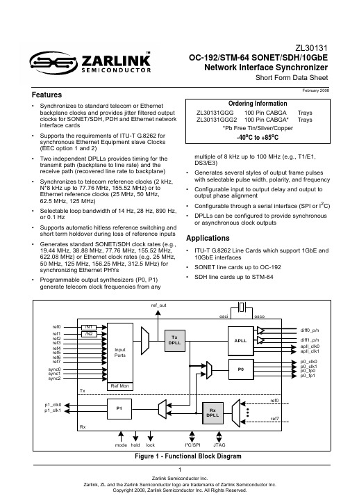
1Features•Synchronizes to standard telecom or Ethernet backplane clocks and provides jitter filtered output clocks for SONET/SDH, PDH and Ethernet network interface cards•Supports the requirements of ITU-T G.8262 for synchronous Ethernet Equipment slave Clocks (EEC option 1 and 2)•Two independent DPLLs provides timing for the transmit path (backplane to line rate) and the receive path (recovered line rate to backplane) •Synchronizes to telecom reference clocks (2kHz, N*8kHz up to 77.76MHz, 155.52MHz) or to Ethernet reference clocks (25MHz, 50MHz, 62.5MHz, 125MHz)•Selectable loop bandwidth of 14Hz, 28Hz, 890Hz, or 0.1Hz•Supports automatic hitless reference switching and short term holdover during loss of reference inputs •Generates standard SONET/SDH clock rates (e.g., 19.44MHz, 38.88MHz, 77.76MHz, 155.52MHz, 622.08MHz) or Ethernet clock rates (e.g. 25MHz, 50MHz, 125MHz, 156.25MHz, 312.5MHz) for synchronizing Ethernet PHYs•Programmable output synthesizers (P0, P1) generate telecom clock frequencies from anymultiple of 8kHz up to 100MHz (e.g., T1/E1, DS3/E3)•Generates several styles of output frame pulses with selectable pulse width, polarity, and frequency •Configurable input to output delay and output to output phase alignment•Configurable through a serial interface (SPI or I 2C)•DPLLs can be configured to provide synchronous or asynchronous clock outputsApplications•ITU-T G.8262 Line Cards which support 1GbE and 10GbE interfaces•SONET line cards up to OC-192•SDH line cards up to STM-64February 2008Figure 1 - Functional Block DiagramZL30131OC-192/STM-64 SONET/SDH/10GbENetwork Interface SynchronizerShort Form Data SheetOrdering InformationZL30131GGG 100 Pin CABGA TraysZL30131GGG2 100 Pin CABGA*Trays*Pb Free Tin/Silver/Copper-40o C to +85o CZL30131Short Form Data Sheet Pin DescriptionPin # Name I/OType DescriptionInput ReferenceC1 B2 A3 C3 B3 B4 C4 A4ref0ref1ref2ref3ref4ref5ref6ref7I u Input References 7:0 (LVCMOS, Schmitt Trigger). These input references areavailable to both the Tx DPLL and the Rx DPLL for synchronizing output clocks.All eight input references can lock to any multiple of 8kHz up to 77.76MHzincluding 25MHz and 50MHz. Input ref0 and ref1 have additional configurablepre-dividers allowing input frequencies of 62.5MHz, 125MHz, and 155.52MHz.These pins are internally pulled up to V dd.B1 A1 A2sync0sync1sync2I u Frame Pulse Synchronization References 2:0 (LVCMOS, Schmitt Trigger).These are optional frame pulse synchronization inputs associated with inputreferences 0, 1 and 2. These inputs accept frame pulses in a clock format (50%duty cycle) or a basic frame pulse format with minimum pulse width of 5 ns.These pins are internally pulled up to V dd.Output Clocks and Frame PulsesA9 B10diff0_pdiff0_nO Differential Output Clock 0 (LVPECL). When in SONET/SDH mode, this output can be configured to provide any one of the available SONET/SDH clocks(6.48MHz, 19.44MHz, 38.88MHz, 51.84MHz, 77.76MHz, 155.52MHz,311.04MHz, 622.08MHz). When in Ethernet mode, this output can beconfigured to provide any of the Ethernet clocks (25MHz, 50MHz, 62.5MHz,125MHz, 156.25MHz, 312.5MHz). See “Output Clocks and Frame Pulses”section on page22 more detail on clock frequency settings.A10 B9diff1_pdiff1_nO Differential Output Clock 1 (LVPECL). When in SONET/SDH mode, this output can be configured to provide any one of the available SONET/SDH clocks(6.48MHz, 19.44MHz, 38.88MHz, 51.84MHz, 77.76MHz, 155.52MHz,311.04MHz, 622.08MHz). When in Ethernet mode, this output can beconfigured to provide any of the Ethernet clocks (25MHz, 50MHz, 62.5MHz,125MHz, 156.25MHz, 312.5MHz). See “Output Clocks and Frame Pulses”section on page22 more detail on clock frequency settings.D10apll_clk0O APLL Output Clock 0 (LVCMOS). This output can be configured to provide anyone of the SONET/SDH clock outputs up to 77.76MHz or any of the Ethernetclock rates up to 125MHz. The default frequency for this output is 77.76MHz.G10apll_clk1O APLL Output Clock 1 (LVCMOS). This output can be configured to provide anyone of the SONET/SDH clock outputs up to 77.76MHz or any of the Ethernetclock rates up to 125MHz. The default frequency for this output is 19.44MHz.K9p0_clk0O Programmable Synthesizer 0 - Output Clock 0 (LVCMOS). This output can beconfigured to provide any frequency with a multiple of 8kHz up to 100MHz inaddition to 2kHz. The default frequency for this output is 2.048MHz.K7p0_clk1O Programmable Synthesizer 0 - Output Clock 1 (LVCMOS). This is aprogrammable clock output configurable as a multiple or division of the p0_clk0frequency within the range of 2 kHz to 100 MHz. The default frequency for thisoutput is 8.192MHz.K8p0_fp0O Programmable Synthesizer 0 - Output Frame Pulse 0 (LVCMOS). This outputcan be configured to provide virtually any style of output frame pulse associatedwith the p0 clocks. The default frequency for this frame pulse output is 8kHz.ZL30131Short Form Data SheetJ7p0_fp1OProgrammable Synthesizer 0 - Output Frame Pulse 1 (LVCMOS). This output can be configured to provide virtually any style of output frame pulse associated with the p0 clocks. The default frequency for this frame pulse output is 8kHz J10p1_clk0OProgrammable Synthesizer 1 - Output Clock 0 (LVCMOS). This output can be configured to provide any frequency with a multiple of 8kHz up to 100MHz in addition to 2kHz. The default frequency for this output is 1.544MHz (DS1).K10p1_clk1OProgrammable Synthesizer1 - Output Clock 1 (LVCMOS). This is a programmable clock output configurable as a multiple or division of the p1_clk0frequency within the range of 2kHz to 100MHz. The default frequency for this output is 3.088MHz (2x DS1).E1ref_out ORx DPLL Selected Output Reference (LVCMOS). This is a buffered copy of the output of the reference selector for the Rx DPLL. Switching between input reference clocks at this output is not hitless.Control H5rst_bIReset (LVCMOS, Schmitt Trigger). A logic low at this input resets the device. To ensure proper operation, the device must be reset after power-up. Reset should be asserted for a minimum of 300ns.J5hs_enI uTx DPLL Hitless Switching Enable (LVCMOS, Schmitt Trigger). A logic high at this input enables hitless reference switching. A logic low disables hitless reference switching and re-aligns the Tx DPLL’s output phase to the phase of the selected reference input. This feature can also be controlled through software registers. This pin is internally pulled up to Vdd.C2D2mode_0mode_1I uTx DPLL Mode Select 1:0 (LVCMOS, Schmitt Trigger). During reset, the levels on these pins determine the default mode of operation for the Tx DPLL (Automatic, Normal, Holdover or Freerun). After reset, the mode of operation can be controlled directly with these pins, or by accessing the tx_dpll_modesel register (0x1F) through the serial interface. This pin is internally pulled up to Vdd.K1diff0_enI uDifferential Output 0 Enable (LVCMOS, Schmitt Trigger). When set high, the differential LVPECL output 0 driver is enabled. When set low, the differential driver is tristated reducing power consumption. This pin is internally pulled up to Vdd.D3diff1_enI uDifferential Output 1 Enable (LVCMOS, Schmitt Trigger). When set high, the differential LVPECL output 1 driver is enabled. When set low, the differential driver is tristated reducing power consumption.This pin is internally pulled up to Vdd.Status H1lockOLock Indicator (LVCMOS). This is the lock indicator pin for the Tx DPLL. This output goes high when the Tx DPLL’s output is frequency and phase locked to the input reference.J1hold OHoldover Indicator (LVCMOS). This pin goes high when the Tx DPLL enters the holdover mode.Pin # Name I/O Type DescriptionZL30131Short Form Data SheetSerial Interface E2sck_sclI/BClock for Serial Interface (LVCMOS). Serial interface clock. When i2c_en = 0,this pin acts as the sck pin for the serial interface. When i2c_en = 1, this pin acts as the scl pin (bidirectional) for the I 2C interface.F1si_sda I/BSerial Interface Input (LVCMOS). Serial interface data pin. When i2c_en = 0,this pin acts as the si pin for the serial interface. When i2c_en = 1, this pin acts as the sda pin (bidirectional) for the I 2C interface.G1so OSerial Interface Output (LVCMOS). Serial interface data output. When i2c_en =0, this pin acts as the so pin for the serial interface. When i2c_en = 1, this pin is unused and should be left unconnected.E3cs_b_asel0I uChip Select for SPI/Address Select 0 for I 2C (LVCMOS). When i2c_en = 0, this pin acts as the chip select pin (active low) for the serial interface. When i2c_en =1, this pin acts as the asel0 pin for the I 2C interface.F3asel1I uAddress Select 1 for I 2C (LVCMOS). When i2c_en = 1, this pin acts as the asel1 pin for the I 2C interface. Internally pulled up to Vdd. Leave open when not in use.F2asel2I uAddress Select 2 for I 2C (LVCMOS). When i2c_en = 1, this pin acts as the asel2 pin for the I 2C interface. Internally pulled up to Vdd. Leave open when not in use.G2int_b OInterrupt Pin (LVCMOS). Indicates a change of device status prompting the processor to read the enabled interrupt service registers (ISR). This pin is an open drain, active low and requires an external pulled-up to Vdd.J2i2c_enI uI 2C Interface Enable (LVCMOS). If set high, the I 2C interface is enabled, if set low, the SPI interface is enabled. Internally pull-up to Vdd.APLL Loop Filter A6apll_filter A External Analog PLL Loop Filter terminal.B6filter_ref0A Analog PLL External Loop Filter Reference.C6filter_ref1AAnalog PLL External Loop Filter Reference.JTAG and Test J4tdoOTest Serial Data Out (Output). JTAG serial data is output on this pin on the falling edge of tck. This pin is held in high impedance state when JTAG scan is not enabled.K2tdiI uTest Serial Data In (Input). JTAG serial test instructions and data are shifted in on this pin. This pin is internally pulled up to Vdd. If this pin is not used then it should be left unconnected.H4trst_bI uTest Reset (LVCMOS). Asynchronously initializes the JTAG TAP controller by putting it in the Test-Logic-Reset state. This pin should be pulsed low on power-up to ensure that the device is in the normal functional state. This pin is internally pulled up to Vdd. If this pin is not used then it should be connected to GND.K3tck ITest Clock (LVCMOS): Provides the clock to the JTAG test logic. If this pin is not used then it should be pulled down to GND.Pin #NameI/O TypeDescriptionZL30131Short Form Data Sheet J3tms I u Test Mode Select (LVCMOS). JTAG signal that controls the state transitions ofthe TAP controller. This pin is internally pulled up to V DD. If this pin is not usedthen it should be left unconnected.Master ClockK4osci I Oscillator Master Clock Input (LVCMOS). This input accepts a 20MHzreference from a clock oscillator (TCXO, OCXO). The stability and accuracy ofthe clock at this input determines the free-run accuracy and the long termholdover stability of the output clocks.K5osco O Oscillator Master Clock Output (LVCMOS). This pin must be left unconnectedwhen the osci pin is connected to a clock oscillator.MiscellaneousJ6IC Internal Connection. Connect to ground.C5B5K6H10IC Internal Connection. Leave unconnected.H7G3E10F10D1NC No Connection. Leave Unconnected.Power and GroundD9 E4 G8 G9 J8 J9 H6 H8V DD PPPPPPPPPositive Supply Voltage. +3.3V DC nominal.E8 F4V CORE PPPositive Supply Voltage. +1.8V DC nominal.A5 A8 C10AV DD PPPPositive Analog Supply Voltage. +3.3V DC nominal.B7 B8 H2AV CORE PPPPositive Analog Supply Voltage. +1.8V DC nominal.Pin # Name I/OType DescriptionZL30131Short Form Data SheetI - InputI d -Input, Internally pulled down I u -Input, Internally pulled up O -Output A -Analog P -Power G -GroundD4D5D6D7E5E6E7F5F6F7G4G5G6G7E9F8F9H9V SSG G G G G G G G G G G G G G G G G G Ground. 0 Volts.A7C7C8C9D8H3AV SSG G G G G GAnalog Ground. 0 Volts.Pin # Name I/O Type DescriptionZL30131Short Form Data Sheet1.0 Pin DiagramBCDEFGHJK234567891011 - A1 corner is identified with a dot.Async1TOP VIEWsync2ref2ref7AV DDapll_filterAV SSAV DDdiff0_pdiff1_psync0ref1ref4ref5ICfilter_ref0AV COREAV COREdiff1_ndiff0_nref0mode_0ref3ref6ICfilter_ref1AV SSAV SSAV SSAV DDNCmode_1diff1_enV SSV SSV SSV SSAV SSV DDapll_clk0ref_outsck/ cs_b/VDDV SSV SSV SSV COREV SSNCsi/asel2asel1V COREV SSV SSV SSV SSV SSNCsoint_bNCV SSV SSV SSV SSV DDV DDapll_clk1lockAV COREAV SStrst_brst_bV DDNCV DDV SSICholdi2c_entmstdohs_enICp0_fp1V DDV DDp1_clk0diff0_entditckoscioscoICp0_clk1p0_fp0p0_clk0p1_clk11scl sdhasel0ZL30131Short Form Data Sheet 2.0 Functional DescriptionThe ZL30131 OC-192/STM-64 PDH/SONET/SDH/10GbE Network Interface Synchronizer is a highly integrated device that provides timing for both PDH/SONET/SDH and Ethernet network interface cards. A functional block diagram is shown in Figure 1.This device is ideally suited for designs that require both a transmit timing path (backplane to PHY) and a receive timing path (PHY to backplane). Each path is controlled with separate DPLLs (Tx DPLL, Rx DPLL) which are both independently configurable through the serial interface (SPI or I2C). A typical application of the ZL30131 is shown in Figure 2. In this application, the ZL30131 translates the 19.44MHz clock from the telecom rate backplane (system timing bus), translates the frequency to 622.08MHz or 156.25MHz for the PHY Tx clock, and filters the jitter to ensure compliance with the related standards. A programmable synthesizer (P0) provides synchronous PDH clocks with multiples of 8kHz for generating PDH interface clocks. On the receive path, the Rx DPLL and the P1 synthesizer translate the line recovered clock (8kHz or 25MHz) from the PHY to the 19.44MHz telecom backplane (line recovered timing) for the central timing cards. The ZL30131 allows easy integration of Ethernet line rates with today’s telecom backplanes.Figure 2 - Typical Application of the ZL30131Information relating to products and services furnished herein by Zarlink Semiconductor Inc. or its subsidiaries (collectively “Zarlink”) is believed to be reliable.However, Zarlink assumes no liability for errors that may appear in this publication, or for liability otherwise arising from the application or use of any such information, product or service or for any infringement of patents or other intellectual property rights owned by third parties which may result from such application or use. Neither the supply of such information or purchase of product or service conveys any license, either express or implied, under patents or other intellectual property rights owned by Zarlink or licensed from third parties by Zarlink, whatsoever. Purchasers of products are also hereby notified that the use of product in certain ways or in combination with Zarlink, or non-Zarlink furnished goods or services may infringe patents or other intellectual property rights owned by Zarlink.This publication is issued to provide information only and (unless agreed by Zarlink in writing) may not be used, applied or reproduced for any purpose nor form part of any order or contract nor to be regarded as a representation relating to the products or services concerned. The products, their specifications, services and other information appearing in this publication are subject to change by Zarlink without notice. No warranty or guarantee express or implied is made regarding the capability, performance or suitability of any product or service. Information concerning possible methods of use is provided as a guide only and does not constitute any guarantee that such methods of use will be satisfactory in a specific piece of equipment. It is the user’s responsibility to fully determine the performance and suitability of any equipment using such information and to ensure that any publication or data used is up to date and has not been superseded. Manufacturing does not necessarily include testing of all functions or parameters. These products are not suitable for use in any medical products whose failure to perform may result in significant injury or death to the user. All products and materials are sold and services provided subject to Zarlink’s conditions of sale which are available on request.Purchase of Zarlink’s I 2C components conveys a licence under the Philips I 2C Patent rights to use these components in and I 2C System, provided that the system conforms to the I 2C Standard Specification as defined by Philips.Zarlink, ZL and the Zarlink Semiconductor logo are trademarks of Zarlink Semiconductor Inc.Copyright Zarlink Semiconductor Inc. All Rights Reserved.TECHNICAL DOCUMENTATION - NOT FOR RESALEFor more information about all Zarlink productsvisit our Web Site at。
ZL30310GKG中文资料(microsemi)中文数据手册「EasyDatasheet - 矽搜」
一个完整设计手册是提供给符合条件客户. 要进行注册,请发送电子邮件至
特征 • 恢复和传输网络同步
通过以太网,IP和MPLS网络 • 同时支持同步
以太网和IEEE1588行业标准时序
协议
• 功能服务器,客户端和中继器操作 • 集成两个独立数字锁相环,
与包和电之间无缝切换 时钟基准
-40°C至+ 85°C
• 生成两个独立同步以太网 钟表推动行业标准以太网PHY 在任25 MHz或125 MHz设备
• 完全可配置解决方案,使性能 进行调整以适应应用/网络要求
• 两个可独立配置MAC接口, 支持MII,RMII,GMII和TBI标准
• 线速以太网桥通过功能 在MAC接口之间
• 同步串行控制接口
卓联结合两种方法到单个设备.该ZL30310集成一个极低抖动 频率合成器,能够产生所需所有同步以太网操作频率, 加上卓联公司正在申请专利时序分组(TOP)技术基础上,行业标准 IEEE1588 TM "PTP"(精密时间协议).它不仅可以作为一个全功能数字锁相环,还 支持时间,相位和频率在这两个第2层和第3层网络分布,同时使用 同步以太网和IEEE 1588协议,可以单独或组合使用.
客户端和中继器行为相结合, 例如,IEEE1588中继器
当作为服务器操作系统,卓设备锁定到输入参考时钟作为一个传统PLL, 过滤任何抖动可能存在.它也同步于任何低频对准信号,例如,一个8千赫 TDM帧脉冲或1赫兹对齐输入.该装置可提供数据包流,每个都包含一个时间戳指示精确时间,该分组被发射 到网络中,相对于已获取基准.它还接收报文从客户端,并返回一个消息,指示在服务器接收客户端消息准确时间 .利用这些信息,客户能够调整自己时基与服务器.
国产工业级处理器GSC3280数据手册

北京神州龙芯集成电路设计有限公司 版权所有
第I页
GSC3280 数据手册
图Байду номын сангаас录
图 1-1 GSC3280 结构框图........................................................................................................5 图 2-1 GSC3280 LFBGA256 封装顶视图与底视图...................................................................6 图 2-2 GSC3280 LFBGA256 封装侧视图与剖面图...................................................................7 图 2-3 GSC3280 LFBGA256 封装效果图(底视图)...............................................................8 图 3-1 仅使用内部上电复位电路的复位时序.....................................................................27 图 3-2 复位引脚 sys_rstn 外接上电复位电路的复位时序..................................................28 图 3-3 复位引脚 sys_rstn 连接手动复位的复位时序...........................................................28 图 3-4 GSC3280 不同电源域上电顺序 ..................................................................................28 图 4-1 JTAG 工作时序.............................................................................................................29 图 4-2 DDR2 SDRAM 读操作时序 ..........................................................................................30 图 4-3 DDR2 SDRAM 写操作时序 ..........................................................................................31 图 4-4 NAND Flash 控制器写命令时序 .................................................................................31 图 4-5 NAND Flash 控制器写地址时序 .................................................................................32 图 4-6 NAND Flash 控制器写数据时序 .................................................................................32 图 4-7 NAND Flash 控制器读数据时序 .................................................................................32 图 4-8 EMI 读时序参数 ..........................................................................................................33 图 4-9 EMI 读时序图 ..............................................................................................................33 图 4-10 EMI 写时序图 ............................................................................................................34 图 4-11 EMI burst 读时序图...................................................................................................34 图 4-12 EMI burst 写时序图...................................................................................................35 图 4-13 MDIO 接口时序图 .....................................................................................................35 图 4-14 MII 模式发送接口时序图 .........................................................................................36 图 4-15 MII 模式接收接口时序图 .........................................................................................36 图 4-16 RMII 模式接口时序图 ...............................................................................................37 图 4-17 SD/SDIO 接口时序图.................................................................................................38 图 4-18 LCD 接口时序图 ........................................................................................................38 图 4-19 SPI 接口时序图(CPHA=0).....................................................................................39 图 4-20 SPI 接口时序图(CPHA=1).....................................................................................40 图 4-21 I2C 接口时序图 .........................................................................................................42 图 4-22 I2S 接口信号时序图..................................................................................................42
EK8003同步升降压IC
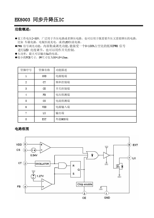
EK8003 同步升降压IC功能概述:◆宽工作电压2-38V,广泛用于升压电路或者降压电路,也可以用于既需要升压又需要降压的电路, 比如 车载电源,电瓶恒流充电,或者LED恒流电源。
◆PWM 信号调光功能:内部集成调光功能,能接受一个0-100%占空比的低频PWM 信号进行LED 亮度调节,也可以用作开关控制。
◆大功率:最大可以输出5A的电流,◆较小的PCB尺寸,5W尺寸仅为30*15*13mm。
管脚序号 管脚名称 功能描述1 GND 电源地端2 CT 频率控制端3 CE 开关控制端4 FB 电压检测端5 CS 电流检测端6 VDD 电源输入端7 LX 输出端8 EXT 外接MOS端电路框图应用1.应用2.应用指南:1) 电压计算:V OUT=1.27x(1+R3/R1),电流计算:I OUT=0.54V/R32) PWM/EN 端(3 脚)可以输入一个100~1000Hz 的低频PWN 信号进行亮度调节,如果不需调光则此端接地。
电感计算:一般来讲在输出相同电压的情况下,输出电流越小电感量要相对加大,而在输出相同电流的情况下,输出电压越高电感量要相对加大。
电感量调整不适当会发生电感响的问题。
4) 输出电容C3的计算:输出电流小的情况下可以用220uF,输出电流为300mA以上建议用470uF或者更大容量的电容,电容量小也会发生电感响的问题。
极限参数:参数 符号 测试条件件 最小值典型值 最大值 单位 工作频率 Fosc Ta=25℃ 20 300 KHz 工作电压 Vcc 2 38 V IC 各端极限电压 Vmax 38 V CE脚ON V CE0 1 V CE脚OFF V CE 2 38 V 电压检测端 V FB Ta=25℃ 1.24 1.27 1.3 V 调光频率 F PWM 100 500 1000 Hz LX最大输出电流 Iout 700 mA 电流检测端 SEN Vcc=3-36V Vpin3>V EN 0.510.54 0.57 mV 工作温度范围 Topr - 40 85 ℃储存环境温度 Tstg - 65 150 ℃焊接温度250±5℃ 260℃,10s抗静电强度 2000V 封装尺寸。
- 1、下载文档前请自行甄别文档内容的完整性,平台不提供额外的编辑、内容补充、找答案等附加服务。
- 2、"仅部分预览"的文档,不可在线预览部分如存在完整性等问题,可反馈申请退款(可完整预览的文档不适用该条件!)。
- 3、如文档侵犯您的权益,请联系客服反馈,我们会尽快为您处理(人工客服工作时间:9:00-18:30)。
• Handles up to -6 dB acoustic echo return loss
• 127 ms acoustic echo canceller
• Provides up to 12 dB of Noise Reduction
• Operate in two modes, Dual Analog mode and single Analog mode (other port is digital PCM)
The AEC uses an advanced adaptive filter algorithm that is double-talk stable, allowing convergence even while both parties are talking. This algorithm continually tracks changes in the echo path, regardless of double-talk, as long as a reference signal is available for the echo canceller.
• PCM Data Formats in single Port mode- 16-bit Linear, companded ITU-T A-law or U-law
• Advanced NLP design - full duplex speech with no switched loss on audio paths
MT93L16
ZL38001
ZL38002
ZL38003
Description AEC for analog hands- AEC for analog hands- AEC with noise reduction for digital
free communication
free communication hands-free communication
• Tracks changing echo environment quickly
• Adaptation algorithm converges even during Double-Talk
• Designed for performance in high background noise environments
AEC with noise reduction & codecs for digital hands-free communication
Application Analog Desktop phone Analog Desktop phone Hands-free Car Kits
Hands-free Car Kits
1 channel
1 channel
1 channel
1 channel
LEC
1 channel
1 channel
Custom Load
Custom Load
Gains
User Gain
User Gain/18 dB Gain on Sout
User Gain + System tuning gains
2
Zarlink Semiconductor Inc.
ZL38003
Data Sheet
2.0 Acoustic Echo Canceller (AEC) Description
The AEC section is comprised of an acoustic echo canceller, noise reduction and the operational control functions for operation. The AEC guarantees clear signal transmission in both transmit and receive audio path directions ensuring reliable voice communication even when low level signals are provided. The AEC does not use variable attenuators during double-talk or single-talk periods of speech, as do many other acoustic echo cancellers for speakerphones. Instead, the AEC provides high performance full-duplex operation similar to network echo cancellers. This results in users experiencing clear speech and uninterrupted background signals during the conversation and prevents subjective sound quality problems associated with “noise gating” or “noise contrasting”.
Applications
• Hands-free car kits • Full duplex speaker-phone for digital telephone • Echo cancellation for video conferences • Intercom Systems • Security Systems
User Gain + System tuning gains
Noise
N
N
Y
Y
Reduction
Integrated
N
N
N
Codecs
dual channel
Table 1 - Acoustic Echo Cancellation Family
1.0 Functional Description
The ZL38003 is an Acoustic Echo Canceller (AEC) with dual codec as shown in Figure 2. The ZL38003 provides 127 ms of acoustic echo cancellation, which makes it ideal for hand free car kits, and speaker phones designs. Each of the codecs in the dual codec can be connected to 1 of 4 four analog ports through a cross point switch. Also, the network side can be routed to a digital PCM interface that input/outputs either linear 2's complement or A-/mu law commanded PCM data.
G.711/712 recommendations • Four Audio TX/RX Interfaces • Differential Microphone Inputs • Programmable Bias Voltage Output for Electret
microphones • Microphone Presence Detection, Microphone
• Differential Earpiece Driver Outputs (66 mW rms into 32 Ohms, 150 mW rms into 16 Ohms) • Cross-Point Connects PCM Channels to any of the Four Audio TX/RX Interfaces
**Pb Free Tin/Silver/Copper -40°C to +85°C
• Howling prevention eliminates uncontrolled oscillation in high loop gain conditions
• AGC on speaker path • Transparent data transfer and mute options • Boot loadable for future factory software upgrades • Serial micro-controller interface • Two 16 bit linear ACD and DAC that meet ITU-T
• Multiple Gain pad settings • Adjustable gain pads from -24 dB to +21 dB at Xin, Sin and Sout to compensate for different system requirements • Programmable Microphone Gain (0dB to +46.5 dB in 1.5 dB Steps) • Side tone Mute, Programmable Side tone Gain (-39 dB to +6 dB in 3 dB Steps) • User gain control provided for speaker path (-24 dB to +21 dB in 3 dB steps) • Programmable Earpiece Gain (-28 dB to +2 dB in 2 dB Steps) • RX Channel Mute, Programmable RX Volume control (-21 dB to 0 dB in 3 dB Steps)