中大功率CFL驱动芯片DX6206(Ver 1.2)
双面芯片抵抗元DSC系列

0.7
0.4±0.2
1.7
0.4±0.15
10
2010
5.1±0.3 2.5±0.2
0.8
0.6±0.3
3.0
0.6±0.25
42
2512
6.5±0.3 3.2±0.2
0.8
0.6±0.3
4.4
0.6±0.25
65
C
A
B
L
A
T W
Wrap-around terminations (3 faces)
Construction
Dimensions (mm) & Weight (mg)
L
W
T max
A
B min
C
Wt.
0603
1.6±0.1 0.8±0.1
0.6 0.3±0.15
0.6 0.3±0.15 2.7
0805 2.0±0.15 1.25±0.15 0.7 0.3±0.15 0.9
0.3±0.1
5.0
1206
3.2±0.2 1.6±0.2ctronics reserves the right to make changes in product specification without notice or liability. All information is subject to TT Electronics’ own data and is considered accurate at time of going to print.
DDouobule-bSlidee-dSChidipeRdesistors DCSChSeirpies Resistors
Welwyn Components
L6206中文资料

1/23L6206September 2003 s OPERATING SUPPLY VOLTAGE FROM 8 TO 52V s 5.6A OUTPUT PEAK CURRENT (2.8A DC)s R DS(ON) 0.3Ω TYP. VALUE @ T j = 25 °C s OPERATING FREQUENCY UP TO 100KHz sPROGRAMMABLE HIGH SIDE OVERCURRENT DETECTION AND PROTECTION s DIAGNOSTIC OUTPUT s PARALLELED OPERATIONs CROSS CONDUCTION PROTECTION s THERMAL SHUTDOWNs UNDER VOLTAGE LOCKOUTsINTEGRATED FAST FREE WHEELING DIODESTYPICAL APPLICATIONSs BIPOLAR STEPPER MOTOR s DUAL OR QUAD DC MOTORDESCRIPTIONThe L6206 is a DMOS Dual Full Bridge designed for motor control applications, realized in MultiPower-BCD technology, which combines isolated DMOS Power Transistors with CMOS and bipolar circuits on the same chip. Available in PowerDIP24 (20+2+2),PowerSO36 and SO24 (20+2+2) packages, the L6206 features thermal shutdown and a non-dissipa-tive overcurrent detection on the high side Power MOSFETs plus a diagnostic output that can be easily used to implement the overcurrent protection.BLOCK DIAGRAMDMOS DUAL FULL BRIDGE DRIVERL62062/23ABSOLUTE MAXIMUM RATINGSRECOMMENDED OPERATING CONDITIONSSymbol ParameterTest conditionsValue Unit V S Supply VoltageV SA = V SB = V S60V V ODDifferential Voltage between VS A , OUT1A , OUT2A , SENSE A and VS B , OUT1B , OUT2B , SENSE BV SA = V SB = V S = 60V;V SENSEA = V SENSEB = GND 60VOCD A ,OCD B OCD pins Voltage Range -0.3 to +10V PROGCL A ,PROGCL B PROGCL pins Voltage Range -0.3 to +7V V BOOT Bootstrap Peak VoltageV SA = V SB = V SV S + 10V V IN ,V EN Input and Enable Voltage Range -0.3 to +7V V SENSEA, V SENSEB Voltage Range at pins SENSE A and SENSE B-1 to +4V I S(peak)Pulsed Supply Current (for each V S pin), internally limited by the overcurrent protection V SA = V SB = V S ;t PULSE < 1ms 7.1AI S RMS Supply Current (for each V S pin)V SA = V SB = V S 2.8A T stg , T OPStorage and Operating Temperature Range-40 to 150°CSymbol ParameterTest ConditionsMIN MAX Unit V S Supply VoltageV SA = V SB = V S852V V ODDifferential Voltage Between VS A , OUT1A , OUT2A , SENSE A and VS B , OUT1B , OUT2B , SENSE BV SA = V SB = V S ;V SENSEA = V SENSEB 52VV SENSEA, V SENSEB Voltage Range at pins SENSE A and SENSE B (pulsed t W < t rr )(DC)-6-161V V I OUT RMS Output Current2.8A T j Operating Junction T emperature -25+125°C f swSwitching Frequency100KHz3/23L6206THERMAL DATA(5) The slug is internally connected to pins 1,18,19 and 36 (GND pins).Symbol DescriptionPowerDIP24SO24PowerSO36Unit R th-j-pins MaximumThermal Resistance Junction-Pins 1814-°C/W R th-j-case Maximum Thermal Resistance Junction-Case --1°C/W R th-j-amb1MaximumThermal Resistance Junction-Ambient 1(1)Mounted on a multi-layer FR4 PCB with a dissipating copper surface on the bottom side of 6 cm 2 (with a thickness of 35 µm).4351-°C/W R th-j-amb1Maximum Thermal Resistance Junction-Ambient 2(2)Mounted on a multi-layer FR4 PCB with a dissipating copper surface on the top side of 6 cm 2 (with a thickness of 35 µm).--35°C/W R th-j-amb1MaximumThermal Resistance Junction-Ambient 3(3)Mounted on a multi-layer FR4 PCB with a dissipating copper surface on the top side of 6 cm 2 (with a thickness of 35 µm), 16 via holes and a ground layer.--15°C/W R th-j-amb2Maximum Thermal Resistance Junction-Ambient 4(4)Mounted on a multi-layer FR4 PCB without any heat sinking surface on the board.587762°C/WL62064/23PIN DESCRIPTIONPACKAGENameTypeFunctionSO24/PowerDIP24PowerSO36PIN #PIN #110IN1A Logic input Bridge A Logic Input 1.211IN2A Logic input Bridge A Logic Input 2.312SENSE A Power Supply Bridge A Source Pin. This pin must be connected to Power Ground directly or through a sensing power resistor.413OCD AOpen Drain OutputBridge A Overcurrent Detection and thermal protection pin. An internal open drain transistor pulls to GND whenovercurrent on bridge A is detected or in case of thermal protection.515OUT1A Power OutputBridge A Output 1.6, 7,18, 191, 18,19, 36GNDGNDSignal Ground terminals. In Power DIP and SO packages, these pins are also used for heat dissipation toward the PCB.822OUT1B Power Output Bridge B Output 1.924OCD BOpen Drain OutputBridge B Overcurrent Detection and thermal protection pin. An internal open drain transistor pulls to GND whenovercurrent on bridge B is detected or in case of thermal protection.1025SENSE B Power Supply Bridge B Source Pin. This pin must be connected to Power Ground directly or through a sensing power resistor.1126IN1B Logic Input Bridge B Input 11227IN2B Logic Input Bridge B Input 21328PROGCL BR PinBridge B Overcurrent Level Programming. A resistor connected between this pin and Ground sets theprogrammable current limiting value for the bridge B. By connecting this pin to Ground the maximum current is set. This pin cannot be left non-connected.1429EN B Logic InputBridge B Enable. LOW logic level switches OFF all Power MOSFETs of Bridge B.If not used, it has to be connected to +5V.1530VBOOT Supply Voltage Bootstrap Voltage needed for driving the upper Power MOSFETs of both Bridge A and Bridge B.1632OUT2B Power Output Bridge B Output 2.1733VS B Power Supply Bridge B Power Supply Voltage. It must be connected to the supply voltage together with pin VS A .204VS A Power Supply Bridge A Power Supply Voltage. It must be connected to the supply voltage together with pin VS B .215OUT2APower OutputBridge A Output 2.5/23L6206PACKAGENameTypeFunctionSO24/PowerDIP24PowerSO36PIN #PIN #227VCP Output Charge Pump Oscillator Output.238EN ALogic InputBridge A Enable. LOW logic level switches OFF all Power MOSFETs of Bridge A.If not used, it has to be connected to +5V.249PROGCL AR PinBridge A Overcurrent Level Programming. A resistor connected between this pin and Ground sets theprogrammable current limiting value for the bridge A. By connecting this pin to Ground the maximum current is set. This pin cannot be left non-connected.ELECTRICAL CHARACTERISTICS(T amb = 25 °C, V s = 48V, unless otherwise specified)SymbolParameter Test ConditionsMin Typ Max Unit V Sth(ON)Turn-on Threshold 6.677.4V V Sth(OFF)Turn-off Threshold5.66 6.4V I S Quiescent Supply Current All Bridges OFF;T j = -25°C to 125°C (6)510mA T j(OFF)Thermal Shutdown Temperature165°COutput DMOS Transistors R DS(ON)High-Side Switch ON Resistance T j = 25 °C0.340.4ΩT j =125 °C (6)0.530.59ΩLow-Side Switch ON ResistanceT j = 25 °C 0.280.34ΩT j =125 °C (6)0.470.53ΩI DSSLeakage CurrentEN = Low; OUT = V S 2mA EN = Low; OUT = GND-0.15mASource Drain Diodes V SD Forward ON Voltage I SD = 2.8A, EN = LOW 1.15 1.3V t rr Reverse Recovery Time I f = 2.8A300ns t frForward Recovery Time200nsLogic Input V IL Low level logic input voltage -0.30.8V V IH High level logic input voltage 27V I ILLow Level Logic Input CurrentGND Logic Input Voltage-10µAPIN DESCRIPTION (continued)L62066/23(7)See Fig. 1.(8)See Fig. 2.I IH High Level Logic Input Current 7V Logic Input Voltage10µA V th(ON)Turn-on Input Threshold 1.8 2.0V V th(OFF)Turn-off Input Threshold 0.8 1.3V V th(HYS)Input Threshold Hysteresis0.250.5VSwitching Characteristics t D(on)EN Enable to out turn ON delay time (7)I LOAD =2.8A, Resistive Load 100250400ns t D(on)IN Input to out turn ON delay time I LOAD =2.8A, Resistive Load(dead time included) 1.6µs t RISE Output rise time (7)I LOAD =2.8A, Resistive Load40250ns t D(off)EN Enable to out turn OFF delay time (7)I LOAD =2.8A, Resistive Load 300550800ns t D(off)IN Input to out turn OFF delay time I LOAD =2.8A, Resistive Load 600ns t FALL Output Fall Time (7)I LOAD =2.8A, Resistive Load40250ns t dt Dead Time Protection 0.51µs f CPCharge pump frequency-25°C<T j <125°C0.61MHzOver Current Detection ELECTRICAL CHARACTERISTICS (continued)(T amb = 25 °C, V s = 48V, unless otherwise specified)Symbol Parameter Test ConditionsMinTypMax UnitL62067/23L62068/23CIRCUIT DESCRIPTIONPOWER STAGES and CHARGE PUMPThe L6206 integrates two independent Power MOS Full Bridges. Each Power MOS has an Rd-son=0.3ohm (typical value @ 25°C), with intrinsic fast freewheeling diode. Cross conduction protection is achieved using a dead time (td = 1µs typical) be-tween the switch off and switch on of two Power MOS in one leg of a bridge.Using N Channel Power MOS for the upper transis-tors in the bridge requires a gate drive voltage above the power supply voltage. The Bootstrapped (Vboot)supply is obtained through an internal Oscillator and few external components to realize a charge pump circuit as shown in Figure 3. The oscillator output (VCP) is a square wave at 600kHz (typical) with 10V amplitude. Recommended values/part numbers for the charge pump circuit are shown in Table1.Table 1. Charge Pump External ComponentsValuesLOGIC INPUTSPins IN1A , IN2A , IN1B , IN2B , EN A and EN B are TTL/CMOS and uC compatible logic inputs. The internal structure is shown in Fig. 4. Typical value for turn-on and turn-off thresholds are respectively Vthon=1.8V and Vthoff = 1.3V.Pins EN A and EN B are commonly used to implement Overcurrent and Thermal protection by connecting them respectively to the outputs OCD A and OCD B ,which are open-drain outputs. If that type of connec-tion is chosen, some care needs to be taken in drivingthese pins. Two configurations are shown in Fig. 5and Fig. 6. If driven by an open drain (collector) struc-ture, a pull-up resistor R EN and a capacitor C EN are connected as shown in Fig. 5. If the driver is a stan-dard Push-Pull structure the resistor R EN and the ca-pacitor C EN are connected as shown in Fig. 6. The resistor R EN should be chosen in the range from 2.2k Ω to 180K Ω. Recommended values for R EN and C EN are respectively 100K Ω and 5.6nF. More infor-mation on selecting the values is found in the Over-current Protection section.Figure 5. EN A and EN B Pins Open CollectorTRUTH TABLEX = Don't careHigh Z = High Impedance OutputC BOOT 220nF C P 10nF R P 100ΩD11N4148D21N4148INPUTSOUTPUTS EN IN1IN2OUT1OUT2L X X High Z High Z H L L GND GND H H L Vs GND H L H GND Vs HHHVsVs9/23L6206NON-DISSIPATIVE OVERCURRENT DETECTION AND PROTECTIONIn addition to the PWM current control, an overcurrent detection circuit (OCD) is integrated. This circuit can be used to provides protection against a short circuit to ground or between two phases of the bridge as well as a roughly regulation of the load current. With this internal over current detection, the external current sense resis-tor normally used and its associated power dissipation are eliminated. Fig. 7 shows a simplified schematic of the overcurrent detection circuit for the Bridge A. Bridge B is provided of an analogous circuit.To implement the over current detection, a sensing element that delivers a small but precise fraction of the out-put current is implemented with each high side power MOS. Since this current is a small fraction of the output current there is very little additional power dissipation. This current is compared with an internal reference cur-rent I REF . When the output current reaches the detection threshold Isover the OCD comparator signals a fault condition. When a fault condition is detected, an internal open drain MOS with a pull down capability of 4mA connected to OCD pin is turned on. Fig. 8 shows the OCD operation.This signal can be used to regulate the output current simply by connecting the OCD pin to EN pin and adding an external R-C as shown in Fig.7. The off time before recovering normal operation can be easily programmed by means of the accurate thresholds of the logic inputs.I REF and, therefore, the output current detection threshold are selectable by R CL value, following the equations:–Isover = 5.6A ±30% at -25°C < T j < 125°C if R CL = 0Ω (PROGCL connected to GND)–Isover = ±10% at -25°C < T j < 125°C if 5K Ω < R CL < 40k ΩFig. 9 shows the output current protection threshold versus R CL value in the range 5k Ω to 40k Ω.The Disable Time t DISABLE before recovering normal operation can be easily programmed by means of the accu-rate thresholds of the logic inputs. It is affected whether by C EN and R EN values and its magnitude is reported inFigure 10. The Delay Time t DELAY before turning off the bridge when an overcurrent has been detected depends only by C EN value. Its magnitude is reported in Figure 11.C EN is also used for providing immunity to pin EN against fast transient noises. Therefore the value of C EN should be chosen as big as possible according to the maximum tolerable Delay Time and the R EN value should be chosen according to the desired Disable Time.The resistor R EN should be chosen in the range from 2.2K Ω to 180K Ω. Recommended values for R EN and C EN are respectively 100K Ω and 5.6nF that allow obtaining 200µs Disable Time.22100R CL----------------L620610/2311/23THERMAL PROTECTIONIn addition to the Ovecurrent Detection, the L6206 integrates a Thermal Protection for preventing the device destruction in case of junction over temperature. It works sensing the die temperature by means of a sensible element integrated in the die. The device switch-off when the junction temperature reaches 165°C (typ. value) with 15°C hysteresis (typ. value).12/23APPLICATION INFORMATIONA typical application using L6206 is shown in Fig. 12. Typical component values for the application are shown in Table 2. A high quality ceramic capacitor in the range of 100 to 200 nF should be placed between the power pins (VS A and VS B) and ground near the L6206 to improve the high frequency filtering on the power supply and reduce high frequency transients generated by the switching. The capacitors connected from the EN A/OCD A and EN B/OCDB nodes to ground set the shut down time for the Brgidge A and Bridge B respectively when an over current is detected (see Overcurrent Protection). The two current sources (SENSE A and SENSE B) should be connected to Power Ground with a trace length as short as possible in the layout. To increase noise immu-nity, unused logic pins are best connected to 5V (High Logic Level) or GND (Low Logic Level) (see pin descrip-tion). It is recommended to keep Power Ground and Signal Ground separated on PCB.Table 2. Component Values for Typical ApplicationC1100uF D11N4148C2100nF D21N4148C BOOT220nF R CLA5KΩC P10nF R CLB5KΩC ENA 5.6nF R ENA100kΩC ENB 5.6nF R ENB100kΩC REF68nF R P100Ω13/23PARALLELED OPERATIONThe outputs of the L6206 can be paralleled to increase the output current capability or reduce the power dissi-pation in the device at a given current level. It must be noted, however, that the internal wire bond connections from the die to the power or sense pins of the package must carry current in both of the associated half bridges. When the two halves of one full bridge (for example OUT1A and OUT2A) are connected in parallel, the peak current rating is not increased since the total current must still flow through one bond wire on the power supply or sense pin. In addition the over current detection senses the sum of the current in the upper devices of each bridge (A or B) so connecting the two halves of one bridge in parallel does not increase the over current detec-tion threshold.For most applications the recommended configuration is Half Bridge 1 of Bridge A paralleled with the Half Bridge 1 of the Bridge B, and the same for the Half Bridges 2 as shown in Figure 13. The current in the two devices connected in parallel will share very well since the R DS(ON) of the devices on the same die is well matched. When connected in this configuration the over current detection circuit, which senses the current in each bridge (A and B), will sense the current in upper devices connected in parallel independently and the sense circuit with the lowest threshold will trip first. With the enables connected in parallel, the first detection of an over current in either upper DMOS device will turn of both bridges. Assuming that the two DMOS devices share the current equally, the resulting over current detection threshold will be twice the minimum threshold set by the resistors R CLA or R CLB in figure 13. It is recommended to use R CLA = R CLB.In this configuration the resulting Bridge has the following characteristics.- Equivalent Device: FULL BRIDGE- R DS(ON) 0.15Ω Typ. Value @ T J = 25°C- 5.6A max RMS Load Current- 11.2A max OCD Threshold14/23To operate the device in parallel and maintain a lower over current threshold, Half Bridge 1 and the Half Bridge 2 of the Bridge A can be connected in parallel and the same done for the Bridge B as shown in Figure 14. In this configuration, the peak current for each half bridge is still limited by the bond wires for the supply and sense pins so the dissipation in the device will be reduced, but the peak current rating is not increased.When connected in this configuration the over current detection circuit, senses the sum of the current in upper devices connected in parallel. With the enables connected in parallel, an over current will turn of both bridges. Since the circuit senses the total current in the upper devices, the over current threshold is equal to the threshold set the resistor R CLA or R CLB in figure 14. R CLA sets the threshold when outputs OUT1A and OUT2A are high and resistor R CLB sets the threshold when outputs OUT1B and OUT2B are high.It is recommended to use R CLA = R CLB.In this configuration, the resulting bridge has the following characteristics.- Equivalent Device: FULL BRIDGE- R DS(ON) 0.15Ω Typ. Value @ T J = 25°C- 2.8A max RMS Load Current- 5.6A max OCD Threshold15/23It is also possible to parallel the four Half Bridges to obtain a simple Half Bridge as shown in Fig. 15. In this configuration the, the over current threshold is equal to twice the minimum threshold set by the resistors R CLA or R CLB in Figure 15. It is recommended to use R CLA = R CLB.The resulting half bridge has the following characteristics.- Equivalent Device: HALF BRIDGE- R DS(ON) 0.075Ω Typ. Value @ T J = 25°C- 5.6A max RMS Load Current- 11.2A max OCD Threshold16/23OUTPUT CURRENT CAPABILITY AND IC POWER DISSIPATIONIn Fig. 16 and Fig. 17 are shown the approximate relation between the output current and the IC power dissipa-tion using PWM current control driving two loads, for two different driving types:–One Full Bridge ON at a time (Fig.16) in which only one load at a time is energized.–Two Full Bridges ON at the same time (Fig.17) in which two loads at the same time are energized. For a given output current and driving type the power dissipated by the IC can be easily evaluated, in order to establish which package should be used and how large must be the on-board copper dissipating area to guar-antee a safe operating junction temperature (125°C maximum).THERMAL MANAGEMENTIn most applications the power dissipation in the IC is the main factor that sets the maximum current that can be de-liver by the device in a safe operating condition. Therefore, it has to be taken into account very carefully. Besides the available space on the PCB, the right package should be chosen considering the power dissipation. Heat sinking can be achieved using copper on the PCB with proper area and thickness. Figures 19, 20 and 21 show the Junction-to-Ambient Thermal Resistance values for the PowerSO36, PowerDIP24 and SO24 packages.For instance, using a PowerSO package with copper slug soldered on a 1.5 mm copper thickness FR4 board with 6cm2 dissipating footprint (copper thickness of 35µm), the R th j-amb is about 35°C/W. Fig. 18 shows mount-ing methods for this package. Using a multi-layer board with vias to a ground plane, thermal impedance can be reduced down to 15°C/W.17/2318/23Figure 22. Typical Quiescent Current vs.Supply VoltageFigure 23. Normalized Typical QuiescentFigure 24. Typical Low-Side R DS(ON) vs.Figure 25. Typical High-Side RDS(ON) vs.Supply VoltageFigure 26. Normalized R DS(ON) vs.JunctionFigure 27. Typical Drain-Source DiodeForward ON Characteristic19/2320/23L620621/23L620622/23L6206 Information furnished is believed to be accurate and reliable. However, STMicroelectronics assumes no responsibility for the consequences of use of such information nor for any infringement of patents or other rights of third parties which may result from its use. No license is grantedby implication or otherwise under any patent or patent rights of STMicroelectronics. Specifications mentioned in this publication are subject to change without notice. This publication supersedes and replaces all information previously supplied. STMicroelectronics products are notauthorized for use as critical components in life support devices or systems without express written approval of STMicroelectronics.The ST logo is a registered trademark of STMicroelectronics.All other names are the property of their respective owners© 2003 STMicroelectronics - All rights reservedSTMicroelectronics GROUP OF COMPANIESAustralia - Belgium - Brazil - Canada - China - Czech Republic - Finland - France - Germany - Hong Kong - India - Israel - Italy - Japan - Malaysia - Malta - Morocco - Singapore - Spain - Sweden - Switzerland - United Kingdom - United States23/23。
RM6206中文规格书-20130311

电流源,能使RM6206振荡的最小电流源
反馈防上限电流: 在常态下,当
电流;
VFB=6V,VIS=0.3V时,流入FB脚的电流;
启动电压: 上述条件下,能使RM6206振荡
内部反馈电源电压: 在常态下,当RM6206
的最大VCC电压;
无反馈电路时VCC脚的电压;
再启动电压:上述条件下,能使RM6206振
2013-03-11
3
电气特性
测试条件: T=25℃,,VCC=5.5-7.5V, Ct=680PF, RS=1Ω;
参数
符号
条件
输出
开关管最大耐压
IOC=10mA
饱和压降 输出上升时间 输出下降时间 输出限制电流
VS A T
Ioc=250mA
TR
CL=1nF
OC上限电流: VFB=6V,FB下拉电流开始动
荡的最小VCC电压;
作时OC流过的最小电流
振荡器关断电压: 上述条件下,能使振荡
器关断的VCC电压;
静态电流: FB脚外接1K欧姆电阻到地,流
2013-03-11
6
封装信息
RM6206
DIP-8
符号
炉等);
2013-03-11
1
典型应用:
RM6206
2013-03-11
2
管脚分布:
RM6206
管脚定义:
管脚 1 2 3 4 5 6
7、8
符号 OB VCC GND FB IS NC OC
功能描述 功率管基极,启动电流输入脚,外接启动电阻到高压直流端
电源输入脚 接地脚
电压反馈脚 电流侦测脚
高频课程设计报告_调频发射机
高频课程设计报告_调频发射机目录1. 内容概述 (2)1.1 课程背景 (3)1.2 报告目的 (3)1.3 报告结构 (4)2. 调频发射机概述 (5)2.1 调频通信原理 (6)2.2 调频发射机组成 (7)3. 调频发射机设计要求 (8)3.1 系统指标 (10)3.2 性能要求 (11)4. 设计方案与实现 (11)4.1 发射机结构设计 (13)4.2 高频电路设计 (14)4.3 调制和解调电路设计 (15)4.4 电源模块设计 (17)5. 调试与优化 (19)5.1 测试方法 (21)5.2 调试过程 (22)5.3 性能优化 (23)6. 测试结果与分析 (25)6.1 发射功率 (26)6.2 频谱纯度 (27)6.3 调制质量 (28)6.4 系统稳定性 (30)7. 结论与展望 (31)7.1 设计总结 (32)7.2 存在问题 (34)7.3 未来改进方向 (35)1. 内容概述本报告详细介绍了调频发射机的高频课程设计,围绕其工作原理、设计要点、实现路径以及未来改进方向展开深入探讨。
从调频发射机的基本原理出发,我们讨论了信号调制、载波频率的调整以及功率放大等关键技术点。
报告紧密结合实际工程需求,详尽阐述了调频发射机的工作著魔步骤和各个模块的功能设计,包括射频前端、调制器、功率放大器等核心部件。
在分析过程中,我们考虑了复杂信号环境下的抗干扰性设计,确保信号传输的稳定性和清晰度。
通过对调频发射机的仿真和数据分析,本报告优化了不同负载条件下的性能表现,为实际生产提供了有效的理论支持。
本课程设计报告还包括了项目实施过程中的遇到的挑战和解决方案,同时讨论了调频发射机在现代无线通信技术中的应用及其市场潜力。
报告最后展望了的未来科技发展趋势,提出了进一步提升调频发射机性能的潜在技术和创新方向。
通过本报告的学习与应用,读者能够获得关于高频调频发射机设计过程的全面了解,并为后续相关研究提供有益的参考和指导。
NXP UBA2211 230V 12W CFL演示板用户手册说明书
UM 10418基于UBA2211的230V 12W CFL演示板版本.2.02——2011 01 10 用户手册文档信息摘要该文档为基于UBA2211的12W演示板用户手册修订历史v.1 10101026 第一版1. 简介UBA2211是一款耐高压集成控制芯片,外部只需增加少量的元件,就能驱动和控制紧凑型荧光灯(CFLs)。
它能为灯正常预热、点火和工作提供所必要的功能。
其内部集成了相关必要的保护功能,具有很高的性价比。
该用户手册将介绍基于UBA2211 230V 12W演示板的应用。
2. 特性2.1 系统集成度●集成半桥功率MOSFET- UBA2211A:导通阻抗13.5欧姆:最大点火电流:0.9A- UBA2211B: 导通阻抗0欧姆:最大点火电流1.35A- UBA2211C: 导通阻抗6.6欧姆:最大点火电流:1.85A●集成自举二极管●集成低压供电电路●集成电平转换电路2.2 灯管寿命●可调的预热时间和点火时间●可调的预热电流,不受电源电压影响●支持冷启动,最小辉光放电时间控制●可调灯功率●灯功率不受电源电压变化影响2.3 安全性●安全启动功能● 50%精确占空比●欠电压自锁保护●电感饱和保护●过热保护●电容模式保护● EOL 保护●灯开路保护2.4 应用简单●可调工作频率,方便与各种灯管匹配3. 电路图典型应用电路如图1图1 紧凑型荧光灯典型应用电路4. 规格说明UBA2211演示板用来驱动12W功率的灯管。
规格说明如下所示:● 230V(AC)−输入电压范围:220V到240V;50Hz−输入功率:230V(AC)下12W−输入电流:230V(AC)下80mA−功率因数:>0.58−正常运行频率:42kHz− 800ms的预热时间●灯管− Baishi 3U 12W灯管−其他灯电压70V,电流150mA的灯管5. 实际应用230V(AC)电源输入和灯管四个输出连接如图2所示:图2 12W CFL UBA2211实际应用6. 电路说明UBA2211为一款集成电路控制芯片,用于驱动紧凑型荧光灯。
CrossChip Microsystems CC6206 全极性锁存型微功耗霍尔效应开关说明书

CC6206全极性锁存型微功耗霍尔效应开关概述CC6206是一颗微功耗、高灵敏度全极性、并具有闩锁输出的霍尔开关传感装置,可直接取代传统的磁簧开关。
特别适用于使用电池电源的便携式电子产品,如行动电话、无绳电话、笔记型电脑、PDA 等。
CC6206具有磁场辨别全极性,亦即只要磁场北极或南极靠近即可启动,磁场撤消后,输出便关闭。
与其他一般霍尔传感装置不同的是并不要特定南极或北极才可以动作,减少了组装时辨别磁极的困扰。
CC6206内部电路包含了霍尔薄片、电压稳压模块、信号放大处理模块、动态失调消除模块、锁存模块以及CMOS 输出级。
由于CC6206使用先进的Bi-CMOS 工艺,整体优化了的线路结构,使得产品获得极低的输入误差反馈。
产品采用了动态失调消除技术,该技术能够消除由封装应力,热应力,以及温度梯度所造成的失调电压,提高器件的一致性。
同时该产品采用及其小型化的封装工艺,使得产品更具极高的性能和市场优势。
CC6206提供TSOT23-3和TO-92S 两种封装,工作温度范围为-40~150℃。
功能框图特点◆工作范围宽,2~5V ◆微功耗◆工作频率为5.5Hz◆全极性输出,对南极和北极磁场均可响应◆良好的温度稳定性◆开关点漂移低◆ESD (HBM )6000V ◆TSOT23-3小尺寸封装应用◆仪器仪表◆PDA ◆笔记本电脑开关输出vs.磁场极性管脚描述极限参数典型应用电路f (H z )VDD(V)VDD(V)扫描频率vs.工作电压静态电流vs.工作电压B (G s )Ta B (G s )VDD(V)磁感应点vs.环境温度磁感应点vs.工作电压(1)TO-92SpackageHall 感应点位置注意:所有单位均为毫米。
打标信息:第一行:CC6206-产品名称第二行:XXYYWWXX –代码YY –封装年份的后两位数WW –封装时的星期数TSOT23-3packageHall 感应点位置注意:所有单位均为毫米。
DX系列中波发射机典型故障速查表
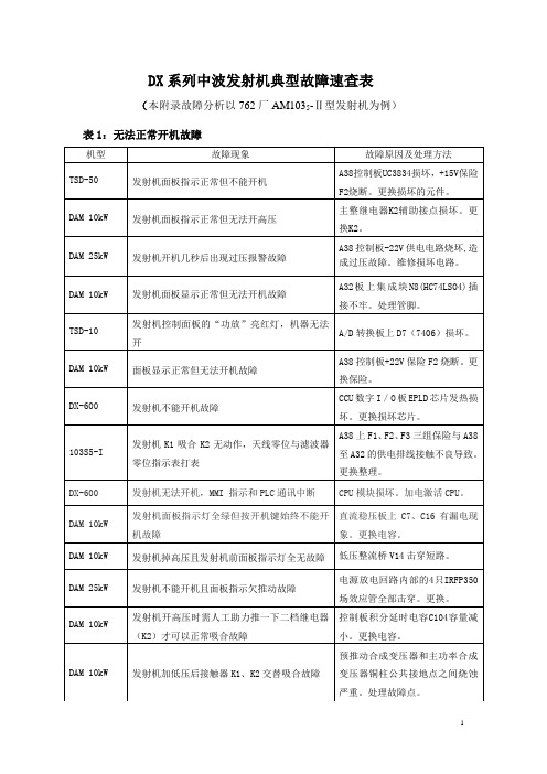
DX系列中波发射机典型故障速查表
(本附录故障分析以762厂AM1035-Ⅱ型发射机为例)表1:无法正常开机故障
表1续:无法正常开机故障
表3:电源故障
表3续:电源故障
表4:联锁故障
表5:自动掉高压故障
表6:过流故障
表7:激励器故障
表8:射频包络故障
表8:射频包络故障
表9:烧功放板故障
表9续:烧功放板故障
表9续:烧功放板故障
表10:冷却故障
表10续:冷却故障
表11:缓冲放大故障
表12:预推动大故障
表13:功率异常故障
表13续:功率异常故障
表13续:功率异常故障
表14:调制编码板故障
表15:直流稳压B+/B-故障
表15续:直流稳压B+/B-故障
表16:失真故障
表17:欠激励、过激励故障
表17续:欠激励、过激励故障
表17续:欠激励、过激励故障
表18:转换错误故障
表18续:转换错误故障
表19:网络驻波故障
表19续:网络驻波故障
表19续:网络驻波故障
表20:其它故障
表20续:其它故障。
2SD315A在高压重复频率电源中的应用

・
8 4・
兵 工 自动 化
第2 9卷
2 D3 5 作 为 一种 适 用 于 中 、 S 1A 大功 率 I T 的 GB 驱动 器 ,输 出驱 动 峰值 电流 达 到 1 5A,具 有 双 极 性 控 制 电压 ( 5v ±1 )的 栅 极 驱 动 ,至 少 1 0k g 0 V/ s的 共模 抑 制 比 , 电气 隔离 特 性 突 出, 抗 干扰 能力 强 。 2 D3 5 内部 结 构 决 定 其 一 个 模 块 可 同 时 触 S 1A 发 2块 I BT3 】 G L4 。 。通 过 MOD ( 式选 择 端 )选 择 模
当 采 用 I T 全 桥 电路 实 现 电源 从 直 流 到 高频 GB 脉 冲 串 的转 变 时 ,通 过 调节 驱 动 电路 2 D3 5 的 S 1A
P WM 输 出 ,可 实 现 电源 高 压 脉 冲 串 的截 止 与 输 出 , 另外也通过改变全桥 P WM 驱 动 脉 冲 的 移 相 角 实现 输 出充 电 电压 ( ~ +2 V)及 充 电速 度 调 节 ,在 0 5k 输 出 端 获 取 理 想 电压 。
g n r t r 2 D31 A a i h  ̄e u n y bi rv u r n n m p r e t l rd r c ho t c r e tf l b c ic i a d e e a o . S 5 h s h g q e c , g d i e c re t a d i e f c i e f ie ts r , u r n o d a k c r u t n b o p we u p y f n to .Ac o d n o is o e a i g p i c p e a d f a u e o o rs p l u ci n c r i g t t p r tn rn i l n e t r ,c mb n o r s p y s s e sr c u e n t e i e p we — u pl y t m tu t r ,o h b s so x e i e t d i e p rp e a i c i a d c r e a i n p r m e e s e i n I c n d i e sn l a v rt i h p we a i fe p rm n , r v e i h r l r u t n o r l to a a t ri sg . t a rv i g e v l eo c d wo h g — o r I GBT i n ̄e u n y 2 k n o r s o d n q e c 0 Hza d c re p n i g i mpu s d h i c n v l i n e i b lt c i v GBT d r c h r c r e t l e wi t , t a a i t a d r l ii a h e eI d y a y ie ts o t u r n f l b c i c i n O o . x e i e t e u ts o d t a h r v ic i h sg o rv a a ii n r t ci n f n to o d a k c r u ta d S n E p rm n s l h we h t e d i e c r u t a o d d i e c p b l y a d p o e t u c i n r t t o i i h p we GBT rv r n h g — o rI d ie . Ke wo d : g o t g ;Hi h p we ; p tt e f e u n y 2 D31 A; i e I y r s Hi h v la e g o r Re e i v r q e c ; S i 5 Drv ; GBT
- 1、下载文档前请自行甄别文档内容的完整性,平台不提供额外的编辑、内容补充、找答案等附加服务。
- 2、"仅部分预览"的文档,不可在线预览部分如存在完整性等问题,可反馈申请退款(可完整预览的文档不适用该条件!)。
- 3、如文档侵犯您的权益,请联系客服反馈,我们会尽快为您处理(人工客服工作时间:9:00-18:30)。
五 典型应用电路
数据手册 1.2 上海登芯微电子有限公司版权所有 -12013-5
大功率 CFL 恒流控制芯片 DX6206
Vbus Cdvdt
DBS
RST
DX6206
CBS
VDD
VB
DVDT
GATEH
Cdc
Lres
GND
VS
CI
GATEL
NC
CS
Lamp CVDD CI
Clamp
Rsense
六 模块框图
4. 超功率
点火结束后进入超功率状态,超功率电感电流设定为 1.3 倍于正常工作阴极电流,超功 率时间内部固定为 50 秒;在进入超功率状态前,如果系统温度高于 90 度,则系统直接 越过超功率状态和过渡状态,进入正常工作状态;在进入超功率状态后,如果系统温度 高于 120 度,则系统直接进入过渡状态。
率与温度
计时振荡器
Tprht Tignmax Tbst Ttr 预热时间 点火时间 超功率时间 过渡时间 0.65 0.75 0.37 50 50 0.85 S S S S
CS 采样
Vref(bn) 正常基准 注1 基准精度 Vref(ocp) Vref(nolamp) Vref(cp) 过流基准 无灯基准 容性基准 650 5 3.1 110 -30 mV % V mV mV
三 应用
大功率室内、外 CFL 应用。
四 订购和标示信息
DX6206 package(ssop10)
DX6206 XXXX
Code1 Code2 Code1 2 3 4 5 Year 2012 2013 2014 2015 Code2 1 2 3 4 Month Jan. Feb. Mar. Apr . Serial No. 6 7 8 9 2016 2017 2018 2019 9 A B C Sep. Oct. Nov. Dec.
8. 容性保护
通过 cs 检测输出电流,判断输出是否进入容性状态,如果进入容性状态,则提升工作频 率以使负载向感性方向移动,最终保持在感性状态,减少半桥中点硬开关,提高系统工 作效率及可靠性。
9. 无灯保护
当输出无灯时,电感电流为零,cs 电压常为低,芯片进入无灯保护状态而停机,直到下 一次重新上电。
压控振荡器
fosc(max) 最大工作频 率 最小工作频 率 最小工作频
Δ
预热状态 其它状态 预热状态 超功率及过渡态 点火及正常状态 Δ T=-20 to +150 °C
82
96 63 63 28
110
kHz kHz kHz kHz
fosc(min)
39
42 2
45
kHz %
fosc(min)/Δ T
VB
VDD
bias
Start logic
DVDT Nolamp & current protect Pulse GND Hsdriver GATEH VS Rms control VCO Deadtime Lsdriver GATEL
CS
CI
七 管脚定义
数据手册 1.2
上海登芯微电子有限公司版权所有 -2-
10. 过温保护
当芯片温度超过 170 度时,进入温度保护状态而停机,直到下一次重新上电清零。
数据手册 1.2
上海登芯微电子有限公司版权所有L 恒流控制芯片 DX6206
VDD
1 2 3 4 5
10 VB 9 GATEH
DVDT GND CI NC
DX6206
8
VS
7 GATEL 6
CS
管脚 1 2 3 4 5 6 7 8 7 10
名称 VDD DVDT GND CI NC CS GATEL VS GATEH VB
九 电气参数
除非特殊说明,否则 TA=25°C。
数据手册 1.2 上海登芯微电子有限公司版权所有 -32013-5
大功率 CFL 恒流控制芯片 DX6206
符号
描述
条件
最小
典型
最大
UNIT
电源
Vdd(start) Vdd(stop) vdd(hys) Vclamp Idd(start) Idd 启动电压 关断电压 迟滞电压 钳位电压 启动电流 工作电流 振荡开始 振荡停止 启动电压-关断电压 Idd=10mA vdd=7.5V Vdd=vdd(start),F=Fmin 11.4 10.5 7.6 11.5 8.4 3.1 12.5 54 1.2 13.6 100 12.5 9.2 V V V V uA mA
时间
大功率 CFL 恒流控制芯片 DX6206
芯片上电点灯过程如上图所示,包括 5 个阶段,出了点火阶段是利用扫频的方式降 低频率,直到点亮灯为止,其它几个状态都是由恒流回路确定。
7. 过流保护
通过 cs 脚检测峰值电流,当峰值电压高于内部设定阈值电压时,发生过流保护,瞬时提 高工作频率以减小阴极电流。
十 应用信息
1. 启动
母线电压通过启动电阻 Rst 向 VCC 电容供电,当 VCC 电压低于启动电压时,芯片处于低 功耗工作模式; 当 VCC 电压高于启动电压时, 芯片开始起振; DVDT 电容将向 VCC 供电, 此时 VCC 电压受内部稳压二极管限制。
Rst
Vbulk min 12.5 I ddstart
驱动
Tdead 死区时间 1.1 uS
温度保护
otp170 停机阈值 温度上升 170
o
C
注 1:基准电压值与工作频率、灯管特性、外围元件等参数有关,该值只用于参考,实际设 计采样电阻需根据灯的功率微调。
数据手册 1.2 上海登芯微电子有限公司版权所有 -42013-5
大功率 CFL 恒流控制芯片 DX6206
描述 低压电源 DVDT 供电输入,外接馈电电容到 HB 信号地 稳定性补偿端口,外接补偿电容到地 空置脚 电流输出及采样端,外接采样电阻到地 下功率管驱动 中点半桥输出 上功率管驱动 高压侧浮动电源
八 绝对最大值范围
如果强度超过下面的极限工作状态很可能会损坏器件。超过这些状态器件可能不运行, 而在推荐的工作条件下器件是能正常运行的, 这些极限工作条件下是不推荐使用的。 下表中 的所有极限电压参数全部是对地的电压,所有的电流是从管脚流进去的电流。另外,超出推 荐工作状态可能会影响器件的可靠性。 符号 VVDD VDT VCI VCS VGATEL VVS VGATEH VVB Tj Tstg 描述 VDD 脚电压 DVDT 脚电压 CI 脚电压 CS 脚电压 GATEL 脚电压 VS 脚电压 GATEH 脚电压 VB 脚电压 最大结温 储藏温度 最小 -0.3 -0.3 -0.3 -5.5 -0.3 -0.3 -0.3 -0.3 -40 -55 典型 最大 12 VVDD+1 5.5 5.5 12 500 500 500 150 150 单位 V V V V V V V V °C °C
2. 预热
芯片启动后首先进入预热状态,工作频率从最高开始,快速降低,直至预热电流达到设 定值; 预热时间内部固定为 0.75s, 预热电感电流内部固定为 1.4 倍于正常工作阴极电流.
3. 点火
预热结束后,系统进入点火状态,频率从预热频率开始向最低频率扫描,直至扫描到最 低工作频率或达到设定点火时间 0.37S,结束点火过程。
大功率 CFL 恒流控制芯片 DX6206
大功率 CFL 恒流控制芯片
一 概述
该芯片应用于大功率紧凑型荧光灯。外围电路非常简单,仅需一个启动电阻、一个自举 供电二极管、一个馈电电容、两个电源旁路电容、一个采样电阻、两个功率 MOS 管、一个 谐振电感、谐振电容及一个隔直电容。 该芯片通过采样电阻采样阴极电流, 放大后控制压控振荡器的输出频率, 从而稳定输出 输出阴极电流,实现恒功率控制。这样就可以实现输入电压变化时保持输出功率恒定。 芯片工作包含如下几种工作模式:预热,阴极电流设计为正常时的 1.4 倍,预热时间为 0.75 秒; 点火频率从预热时所处频率一直向低扫频, 一直达到最低工作频率或者内部计时结 束为止;超功率,电流设置为正常工作时的 1.3 倍,使得灯能快速点亮,超功率时间 50 秒; 过渡,输出从超功率状态逐渐向正常转变,过渡时间 50 秒;正常工作。 各种保护功能:容性保护;无灯保护;过流保护;多级温度保护。 可用封装形式:ssop10。
5. 过渡
超功率结束后,芯片进入过渡工作状态,过渡时间为 50 秒。阴极电流分 16 步,逐级降 低,最终过渡到正常电流值。
6. 正常
过渡状态结束后,芯片进入正常工作状态,系统最低工作频率提高。通过调节系统工作 频率,控制阴极电流恒定。
频 率
预热
超功率
正常 过渡
点 火
芯片启动点灯过程示意图
数据手册 1.2 上海登芯微电子有限公司版权所有 -52013-5
二 特性
快速点亮:50 秒 1.3 倍超功率模式。 无闪烁:在 50 秒内从超功率状态分 16 步逐级降到正常模式。 寿命长:恒流预热;不随电网波动的输出功率。 安全:过温保护;容性保护;无灯保护;过流保护。 使用方便:自适应工作频率。 内部集成齐纳二极管、低压馈电二极管。 恒定电流控制。 微功耗启动(100uA) 。 ssop10 封装、无铅封装。