A3967(步进电机驱动芯片)
基于A3967SLB的步进电机细分驱动系统设计
基于A3967SLB的步进电机细分驱动系统设计传统的细分驱动电路由细分环行分配器、放大器和合成器等部分组成。
这种电路应用复杂,灵活性差。
本文利用a3967slb作为步进电机微控芯片,简化了步进电机的控制实现。
由于单片机资源没有pc丰富,人机界面也没有pc友好,因此,本文采用了主从式结构,即pc用于管理,单片机用于执行。
致芯科技最具实力的芯片解密、IC解密、单片机解密等解密服务机构,致芯科技拥有多年的解密服务经验和超高水平的解密技术,一直从客户利益出发,为每位客户提供最科学最合理最低成本的解密方案与解密服务,深受客户的信赖与喜爱。
a3967slb是美国allegro公司生产的pwm恒流控制微步距驱动二相步进电机专用驱动器。
它的工作电压可达30v,驱动电流达750ma,一个a3967slb即可驱动一台二相步进电机,可实现8细分驱动。
芯片内部的pwm电流控制电路可通过加在pfd的电压设置为慢、快、混合三种电流衰减模式,如果pfd端的电压高于0.6vdd,则选择慢衰减方式。
若低于0.21vdd,则选择快衰减模式。
处于两者之间为混合衰减模式。
另外,a3967slb还能提供完善的保护措施,包括抑制瞬态电压,过热保护、防止电流直通、欠电压自锁等功能。
a3967slb和微处理器之间不需要附加其他的接口电路,该芯片采用easystepper接口,将8条控制线减少了2条,只要简单地输入控制步进电机的脉冲,其内嵌的转换器就可以实现对步进电机的控制。
a3967slb还需要一些电阻、电容来调整其工作参数,整个驱动电路非常简单。
ms1和ms2是步进电机细分分辨率选择的逻辑输入口;dir是电机运转方向的选择口;reset用于重置芯片初始值,屏蔽所有外部输出;step为脉冲输入端口;out1a、out1b、out2a、out2b为h桥的两对输出端口;enable为使能端;sleep为睡眠模式;sense1、sense2为h桥的电流检测电阻;ref为参考电压;gnd为逻辑地和电源地;rc1、rc2为h桥固定截止时间模拟输入。
EasyDriver步进电机驱动器
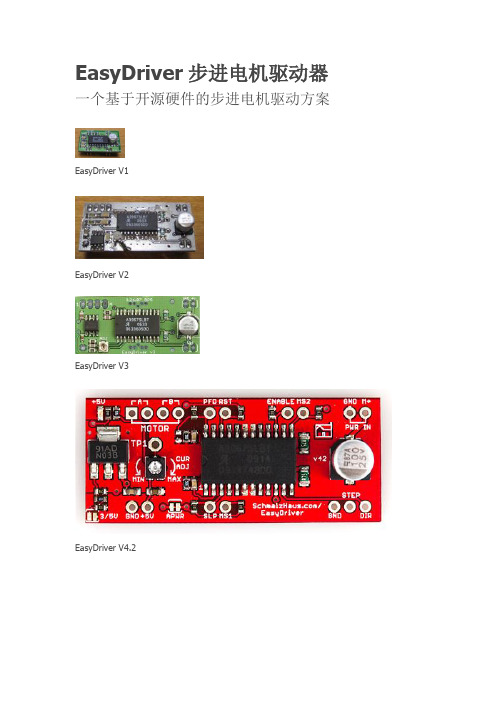
EasyDriver步进电机驱动器一个基于开源硬件的步进电机驱动方案EasyDriver V1EasyDriver V2EasyDriver V3EasyDriver V4.2EasyDriver V4.3EasyDriver V4.4其中V4.2-V4.4在电路上没有区别,改变的仅仅是PCB及丝印内容。
目前网络上售卖的为V4.4,本帖主要介绍EasyDriver的最新版本。
项目简介:Bruce Shapiro找我来搞了个UBW项目(使用USB接口的驱动板),以解决他电脑上没有并行接口的问题。
UBW的设计远超出我的期望。
除了达成最初的设计目标,它同样可以作为其它各种形式的固件的很好的平台。
但还是有个问题!Bruce过去在他的鸡蛋机器人课程上使用UCN5804B步进电机驱动板,因为它很容易配合实验电路板,并且简单易用。
不幸的是,它们现在要17美元一个,还很难找到。
Bruce希望我能设计制作一款同样能搭载在实验电路板上的替代品,仍然只需要两条输入线(步数和方向),能驱动两极步进电机。
于是就有了EasyDriver的设计。
快速指南:每个EasyDriver能够为两级步进电机提供大约每相750mA(两极一共1.5A)的驱动。
它默认设置为8步细分模式(所以如果你的电机是每圈200步,你使用EasyDriver时默认为每圈1600步),更多细分模式可以通过将MS1或MS2两个接脚接地进行设置。
这是一种基于Allegro A3967驱动芯片的细分断路器。
对于此设计的完整规格,请查阅A3967的参数表。
它的最大每相电流从150mA到750mA。
可以采用的最大驱动电压大概是30V,其中包括板载5V的调压器,所以只需要一个电源。
质优价廉,这玩意儿只要10美元,比你自己制作电路板更便宜(广告……)。
我并不出售EasyDriver。
这项设计和UBW一样是免费向公众发布的。
任何人可以参考本页所述的设计方案并随心所欲的改动。
A3967SLB中文资料
A3967中文资料A3967SLTB带转换器的微步进驱动芯片特点±750毫安,30 V额定输出Satlington™灌电流驱动器自动电流衰减模式检测/选择3.0 V至5.5 V逻辑电源电压范围混合,快与慢电流衰减模式内部欠压锁定(UVLO)和热关断电路交叉电流保护描述A3967SLB是一个完善的微电机驱动器内置逻辑器。
它的设计操作双极步进电机具有全步进,1/2,1/4,和1/8模式,输出驱动能力30 V和±750毫安。
A3967SLB包括一个固定关断时间的电流调节器,具有慢,快,或混合电流衰减模式的功能。
此电流衰减控制方案可以减少可听到的电流噪音,增加步进精确度,并减少功耗。
A3967SLB的驱动转换非常容易实现,通过简单的“步进”输入中输入一个脉冲电动机将产生一个步骤(全,半,四分,或八分,这取决于两个逻辑输入)。
无需相位顺序表、高频率控制线或复杂的程序。
该A3967SLB是一个理想的适合复杂的微型项目开发的接口驱动芯片。
内部电路保护包括热关机与滞后,电压锁定(UVLO)下和交叉电流保护。
不需要特别的加电排序。
A3967SLB是提供一个24-PIN SOIC封装,能够自由焊接的磨砂100%雾锡引线框架。
选项卡处于接地电位,并且不需要绝缘。
的无铅(100%雾锡引线框架)版本也已经推出。
绝对最大额定值热特性热特性表电气特性在T A = +25°C,V BB = 30 V,V CC = 3.0 V至5.5V(除非另有说明)功能说明设备操作A3967 是一个操作方便、控制线少、完整的微型步进电机驱动器,。
它可用于双极步进电机在全,半,四分和八分模式的操作。
每两个中的电流 H桥输出的调节与固定关断时间脉冲宽度调制(PWM)控制电路。
在每个步骤中的电流由一个外部的值被设置电流检测电阻(R S),一个参考电压(V REF),以及 DAC 的输出电压的输出,通过控制转换。
在上电或复位时,将根据DAC设置和相电流极性初始的内部状态设置转换(见图内部状态情况),并设定的电流调节器两相混合衰减模式。
easydriver步进电机驱动器(v4.4官网翻译已完成)

EasyDriver步进电机驱动器(V4.4官网翻译,已完成)2015-03-10更新完成。
本帖的全部内容翻译自:/EasyDriver/ 截止日期为2014-04-07,具体更新请见官网。
转载请注明出处:极客工坊-/thread-9234-1-1.html By shenhaiyu 妙娃粽子一个基于开源硬件的步进电机驱动方案EasyDriverV1EasyDriver V2EasyDriver V3EasyDriverV4.2EasyDriver V4.3EasyDriver V4.4其中V4.2-V4.4在电路上没有区别,改变的仅仅是PCB及丝印内容。
目前网络上售卖的为V4.4,本帖主要介绍EasyDriver的最新版本。
项目简介:Bruce Shapiro找我来搞了个UBW项目(使用USB接口的驱动板),以解决他电脑上没有并行接口的问题。
UBW 的设计远超出我的期望。
除了达成最初的设计目标,它同样可以作为其它各种形式的固件的很好的平台。
但还是有个问题!Bruce过去在他的鸡蛋机器人课程上使用UCN5804B步进电机驱动板,因为它很容易配合实验电路板,并且简单易用。
不幸的是,它们现在要17美元一个,还很难找到。
Bruce希望我能设计制作一款同样能搭载在实验电路板上的替代品,仍然只需要两条输入线(步数和方向),能驱动两极步进电机。
于是就有了EasyDriver的设计。
快速指南:每个EasyDriver能够为两级步进电机提供大约每相750mA(两极一共1.5A)的驱动。
它默认设置为8步细分模式(所以如果你的电机是每圈200步,你使用EasyDriver 时默认为每圈1600步),更多细分模式可以通过将MS1或MS2两个接脚接地进行设置。
这是一种基于Allegro A3967驱动芯片的细分断路器。
对于此设计的完整规格,请查阅A3967的参数表。
它的最大每相电流从150mA到750mA。
可以采用的最大驱动电压大概是30V,其中包括板载5V的调压器,所以只需要一个电源。
基于FPGA的PCI从接口设计
《工业控制计算机》2010年23卷第1期随着密度和速度的提高,FPGA (现场可编程门阵列)非常适合实现PCI 总线接口,而且现在许多FPGA 制造商都提供了PCI 接口宏核逻辑(PCI IPCore ),降低了设计难度。
这种方法的最大好处是比较灵活,可以根据实际需求有选择性地实现PCI规范中的功能子集,以后进行功能升级也比较方便,只需重新进行逻辑设计,而且还可以将其他用户逻辑与PCI 接口逻辑集成在一个芯片上,实现紧凑的系统设计。
但是这种方案要求设计者对PCI 总线规范有比较深入的了解,设计难度比使用专用的PCI 接口芯片大一些。
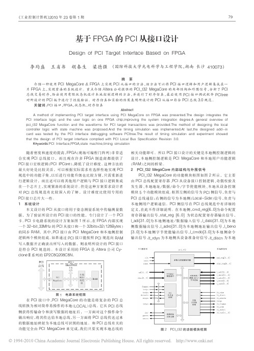
1系统设计本文设计的PCI 从接口将用于姿态测量系统中传输测量数据,为了验证所设计的PCI 接口的性能,专门设计了一个PCI 卡。
PCI 卡电路系统的设计方案如图1所示,在FPGA 内部实现一个32-bit 、33MHz 的PCI 从接口和一个32bits×32(128Bytes )的同步RAM ,其中,PCI 接口由PCI MegaCore 和本地侧控制逻辑两个模块组成。
如果通过PCI 接口能按照PCI 规范向RAM 写入数据并正确读出所写入的数据,则表明所设计的PCI 接口是符合PCI 规范的。
本设计采用的FPGA 是Altera 公司Cy-clone Ⅱ系列的EP2C8Q208C8N 。
图1电路系统框图在PCI 接口中,PCI MegaCore 的功能是将复杂的PCI 总线转换为相对简单易操作的本地(LOCAL )总线。
它从PCI 总线侧获得传输命令和读写数据的地址后,一方面对这个操作命令做出响应,将其传达给本地总线,另一方面将PCI 总线传送过来的数据地址映射为本地总线可识别的地址。
和PCI 总线有关的功能完全由PCI MegaCore 来完成,我们只要实现本地总线的相关功能即可。
所以PCI 接口设计的关键是本地侧控制逻辑的设计,本地侧控制逻辑是PCI MegaCore 和本地用户功能逻辑(RAM )之间的桥梁。
电机驱动电路实训报告
一、实训目的通过本次实训,我旨在深入了解电机驱动电路的原理、设计方法和实际操作技能。
通过对电机驱动电路的搭建、调试和测试,提高自己的电子电路设计、分析和解决问题的能力。
二、实训内容1. 电机驱动电路原理学习本次实训主要学习了直流电机、交流电机和步进电机的驱动电路原理。
直流电机驱动电路主要由电源、电刷、换向器、电枢绕组和电机组成。
交流电机驱动电路主要包括电源、变压器、整流器、滤波器和电机等。
步进电机驱动电路主要由电源、脉冲发生器、驱动芯片和电机组成。
2. 电机驱动电路搭建根据所学原理,我搭建了以下几种电机驱动电路:(1)直流电机驱动电路:采用H桥电路,由四个MOSFET组成。
通过控制MOSFET的通断,实现对直流电机的正反转和调速。
(2)交流电机驱动电路:采用桥式整流电路,将交流电源转换为直流电源,再通过H桥电路驱动电机。
(3)步进电机驱动电路:采用A3967步进电机驱动芯片,通过控制脉冲信号的频率和数量,实现对步进电机的精确定位和转速控制。
3. 电机驱动电路调试在搭建好电机驱动电路后,我对各个电路进行了调试。
首先检查电路连接是否正确,然后对电路参数进行调整,以确保电机能够正常运行。
(1)直流电机驱动电路调试:通过调整PWM信号的占空比,实现对直流电机的调速;通过改变MOSFET的通断,实现电机的正反转。
(2)交流电机驱动电路调试:通过调整整流电路的滤波电容,提高直流电源的稳定性;通过调整H桥电路的驱动电流,实现电机的调速。
(3)步进电机驱动电路调试:通过调整脉冲信号的频率和数量,实现步进电机的精确定位和转速控制。
4. 电机驱动电路测试在调试完成后,我对搭建的电机驱动电路进行了测试。
主要测试内容包括:(1)直流电机驱动电路测试:通过改变PWM信号的占空比,观察电机的转速变化;通过改变MOSFET的通断,观察电机的正反转。
(2)交流电机驱动电路测试:通过改变整流电路的滤波电容,观察直流电源的稳定性;通过改变H桥电路的驱动电流,观察电机的转速变化。
电机驱动芯片选型-步进电机和BLDC-Allegro
厂家型号描述Allegro A3901Dual Full Bridge Low Voltage Motor DriverAllegro A3916Dual DMOS Full-Bridge Motor DriverAllegro A3966Dual Full-Bridge PWM Motor DriverAllegro A3967Microstepping Driver with TranslatorAllegro A3977Microstepping DMOS Driver with TranslatorAllegro A3979Microstepping DMOS Driver with TranslatorAllegro A3981K Automotive, Programmable Stepper DriverAllegro A3982DMOS Stepper Motor Driver with TranslatorAllegro A3983DMOS Microstepping Driver with TranslatorAllegro A3984DMOS Microstepping Driver with TranslatorAllegro A3985Digitally Programmable Dual Full-Bridge MOSFET DriverAllegro A3987DMOS Microstepping Driver with TranslatorAllegro A3988Quad DMOS Full Bridge PWM Motor DriverAllegro A3989Bipolar Stepper and High Current DC Motor DriverAllegro A3992DMOS Dual Full-Bridge Microstepping PWM Motor DriverAllegro A3995DMOS Dual Full Bridge PWM Motor DriverAllegro A3998Dual DMOS Full Bridge Motor Driver With Serial Port Control and Allegro A4970Dual Full-Bridge PWM Motor DriverAllegro A4975Full-Bridge PWM Microstepping Motor DriverAllegro A4979Microstepping Programmable Stepper Motor Driver With Stall Dete Allegro A4980K Automotive, Programmable Stepper DriverAllegro A4982DMOS Microstepping Driver with Translator And Overcurrent Prote Allegro A4983DMOS Microstepping Driver with TranslatorAllegro A4984DMOS Microstepping Driver with Translator And Overcurrent Prote Allegro A4985DMOS Microstepping Driver with Translator And Overcurrent Prote Allegro A4986DMOS Dual Full-Bridge PWM Motor Driver With Overcurrent Protect Allegro A4987DMOS Dual Full-Bridge PWM Motor Driver with Overcurrent Protect Allegro A4988DMOS Microstepping Driver with Translator And Overcurrent Prote Allegro A4989Dual Full-Bridge MOSFET Driver with Microstepping Translator Allegro A4990K Automotive Dual Full Bridge DriveAllegro A4992K Automotive Stepper DriverAllegro A4993Automotive Stepper Motor DriverAllegro A5976Microstepping DMOS Driver with TranslatorAllegro A5977Microstepping DMOS Driver with TranslatorAllegro A5979Microstepping DMOS Driver with TranslatorAllegro A5984DMOS Microstepping Driver with Translator And Overcurrent Prote Allegro A5985DMOS Microstepping Driver with Translator And Overcurrent Prote Allegro A5988Bipolar Stepper and High-Current DC Motor DriverAllegro A5989Bipolar Stepper and High-Current DC Motor DriverAllegro A5990Quad DMOS Full-Bridge PWM Motor DriverAllegro AMT49701Quad DMOS Full-Bridge PWM Motor DriverAllegro AMT49702Dual DMOS Full-Bridge Motor Driver后缀“K”表示汽车级产品(通过 AEC-Q100 认证)下列器件已停产:A3986, A3972电桥数量峰值输出电流最大电源电压接口位置反馈最小电源电压Parallel External 2.5 5.50.4Full-Bridge x2 Parallel External 2.7151Full-Bridge x2 PH/EN External 4.75300.75Full-Bridge x2 Translator (Step/DIR)External 4.75300.85Full-Bridge x2 Translator (Step/DIR)External835 2.5Full-Bridge x2 Translator (Step/DIR)External835 2.5Full-Bridge x2 SPI,Translator (Step/DIR)External732 1.4Full-Bridge x2 Translator (Step/DIR)External8352Full-Bridge x2 Translator (Step/DIR)External8352Full-Bridge x2 Translator (Step/DIR)External8352Full-Bridge x2 SPI External1250Full-Bridge x2 Translator (Step/DIR)External850 1.5Full-Bridge x2 Parallel External836 1.2Full-Bridge x4 Parallel,PH/EN External836 1.2Full-Bridge x4 SPI External1550 1.5Full-Bridge x2 PH/EN External836 2.4Full-Bridge x4 SPI External950 1.5Full-Bridge x2 Parallel External7.45451Full-Bridge x2 Parallel External550 1.5Full-Bridge x1 SPI,Translator (Step/DIR)External750 1.5Full-Bridge x2 SPI,Translator (Step/DIR)External 3.332 1.4Full-Bridge x2 Translator (Step/DIR)External8352Full-Bridge x2 Translator (Step/DIR)External835 2.5Full-Bridge x2 Translator (Step/DIR)External8352Full-Bridge x2 Translator (Step/DIR)External8351Full-Bridge x2 Parallel External8352Full-Bridge x2 Parallel External8351Full-Bridge x2 Translator (Step/DIR)External8352Full-Bridge x2 Translator (Step/DIR)External1250 1.2Full-Bridge x2 Parallel External632 1.4Full-Bridge x2 SPI,Translator (Step/DIR)External 3.832 1.4Full-Bridge x2 SPI,Translator (Step/DIR)Open Loop 3.532 1.4Full-Bridge x2 Translator (Step/DIR)External840 2.8Full-Bridge x2 Translator (Step/DIR)External840 2.8Full-Bridge x2 Translator (Step/DIR)External840 2.8Full-Bridge x2 Translator (Step/DIR)External8402Full-Bridge x2 Translator (Step/DIR)External8402Full-Bridge x2 Parallel External840 1.6Full-Bridge x4 Parallel External840 1.6Full-Bridge x4 Parallel External840 1.6Full-Bridge x4 Parallel External4181Full-Bridge x4 Parallel External 3.5151Full-Bridge x2封装DFN Consumer,Industrial QFN Consumer,Industrial SOIC Consumer,Industrial SOIC Consumer,Industrial TSSOP Consumer,Industrial TSSOP Consumer,Industrial TSSOP AutomotiveSOIC Consumer,Industrial TSSOP Consumer,Industrial TSSOP Consumer,Industrial TSSOP Consumer,Industrial TSSOP Consumer,Industrial QFN,LQFP Consumer,Industrial QFN Consumer,Industrial DIP,TSSOP Consumer,Industrial QFN Consumer,Industrial QFN Consumer,Industrial SOIC Consumer,Industrial DIP,SOIC Consumer,Industrial TSSOP Consumer,Industrial TSSOP AutomotiveQFN,TSSOP Consumer,Industrial QFN Consumer,Industrial QFN,TSSOP Consumer,Industrial QFN,TSSOP Consumer,Industrial QFN,TSSOP Consumer,Industrial QFN,TSSOP Consumer,Industrial QFN Consumer,Industrial TSSOP Consumer,Industrial TSSOP AutomotiveTSSOP AutomotiveTSSOP AutomotiveTSSOP Consumer,Industrial TSSOP Consumer,Industrial TSSOP Consumer,Industrial QFN,TSSOP Consumer,Industrial QFN Consumer,Industrial QFN Consumer,Industrial QFN Consumer,Industrial QFN Consumer,Industrial,Of QFN Consumer,Industrial TSSOP AutomotiveFull, Half Step Resolution, Single Supply, Sleep ModeInternal PWM Current Control, Single Supply, OCP Protection, Fault Output, Sleep Mode, Parallel Ope Internal PWM Current Control, Full, Step Resolution, Sleep ModeInternal PWM Current Control, Full, Half, 1/4, 1/8 Step Resolution, Sleep Mode, Automatic Mixed Dec Internal PWM Current Control, Full, Half, 1/4, 1/8 Step Resolution, Sleep Mode, Automatic Mixed Dec Internal PWM Current Control, Full, Half, 1/4, 1/16 Step Resolution, Sleep Mode, Automatic Mixed De Internal PWM Current Control, Full, Half, 1/4, 1/16 Step Resolution, OCP Protection, Programable Fa Internal PWM Current Control, Full, Half Step Resolution, Sleep Mode, Automatic Mixed DecayInternal PWM Current Control, Full, Half, 1/4, 1/8 Step Resolution, Sleep Mode, Automatic Mixed Dec Internal PWM Current Control, Full, Half, 1/4, 1/16 Step Resolution, Sleep Mode, Automatic Mixed De Internal PWM Current Control, Full, Half, 1/4, 1/16 Step Resolution, Sleep Mode, Mixed Decay Internal PWM Current Control, Full, Half, 1/4, 1/16 Step Resolution, OCP Protection, Sleep Mode, Au Internal PWM Current Control, Full, Half, 1/4 Step Resolution, Automatic Mixed DecayInternal PWM Current Control, Full, Half, 1/4 Step Resolution, Automatic Mixed DecayInternal PWM Current Control, Full, Half, 1/4, 1/16 Step Resolution, OCP Protection, Sleep Mode, Mi Internal PWM Current Control, Automatic Mixed DecayInternal PWM Current Control, Full, Half, 1/4, 1/8 Step Resolution, OCP Protection, Sleep Mode, 3.3 Internal PWM Current Control, Full, Half Step Resolution, Sleep ModeInternal PWM Current Control, Full, Half, 1/4, 1/8 Step Resolution, Automatic Mixed DecayInternal PWM Current Control, Full, Half, 1/4, 1/16 Step Resolution, OCP Protection, Programable Fa Internal PWM Current Control, Full, Half, 1/4, 1/16 Step Resolution, OCP Protection, Programable Fa Internal PWM Current Control, Full, Half, 1/4, 1/16 Step Resolution, OCP Protection, Sleep Mode, Au Internal PWM Current Control, Full, Half, 1/4, 1/8, 1/16 Step Resolution, Sleep Mode, Automatic Mix Internal PWM Current Control, Full, Half, 1/4, 1/8 Step Resolution, OCP Protection, Sleep Mode, Aut Internal PWM Current Control, Full, Half, 1/4, 1/8 Step Resolution, OCP Protection, Sleep Mode, Aut Internal PWM Current Control, Full, Half, 1/4 Step Resolution, OCP Protection, Sleep Mode, Mixed De Internal PWM Current Control, Full, Half, 1/4 Step Resolution, OCP Protection, Sleep Mode, Mixed De Internal PWM Current Control, Full, Half, 1/4, 1/8, 1/16 Step Resolution, OCP Protection, Sleep Mod Internal PWM Current Control, Full, Half, 1/4, 1/16 Step Resolution, Sleep Mode, Mixed Decay Internal PWM Current Control, Full Step Resolution, Single Supply, Sleep ModeInternal PWM Current Control, Full, Half, 1/4, 1/16 Step Resolution, Single Supply, OCP Protection, Integrated Current Sense, Internal PWM Current Control, 50V Transient compatible, Full, Half, 1/4, Internal PWM Current Control, Full, Half, 1/4, 1/16 Step Resolution, OCP Protection, Fault Output, Internal PWM Current Control, Full, Half, 1/4, 1/8 Step Resolution, OCP Protection, Sleep Mode, Aut Internal PWM Current Control, Full, Half, 1/4, 1/16 Step Resolution, OCP Protection, Sleep Mode, Au Internal PWM Current Control, Full, Half, 1/4, 1/8, 1/16, 1/32 Step Resolution, Single Supply, OCP Internal PWM Current Control, Full, Half, 1/4, 1/8, 1/16, 1/32 Step Resolution, Single Supply, OCP Internal PWM Current Control, Full, Half, 1/4 Step Resolution, Single Supply, OCP Protection, Sleep Internal PWM Current Control, Full, Half, 1/4 Step Resolution, Single Supply, OCP Protection, Sleep Adaptive Percent fast decay, Adjustable off time, Internal PWM Current Control, Full, Half, 1/4 Ste Internal PWM Current Control, Full, Half, 1/4 Step Resolution, Single Supply, OCP Protection, Sleep Internal PWM Current Control, Half step resolution, Single Supply, OCP Protection, Fault Output, SlParallel OperationAutomatic Mixed DecayAutomatic Mixed Decay, Automatic Mixed Decaytion, Programable Fault Output, Sleep Mode, Advanced DiagnosticsMixed DecayAutomatic Mixed Decay, Automatic Mixed Decay, Mixed Decaytion, Sleep Mode, Automatic Mixed Decaytion, Sleep Mode, Mixed Decayion, Sleep Mode, 3.3/5.0V LDO, Mixed Decayixed Decaytion, Programable Fault Output, Sleep Mode, Advanced Diagnosticstion, Programable Fault Output, Sleep Mode, Advanced Diagnosticstion, Sleep Mode, Automatic Mixed DecayMode, Automatic Mixed Decayion, Sleep Mode, Automatic Mixed Decayion, Sleep Mode, Automatic Mixed DecaySleep Mode, Mixed DecaySleep Mode, Mixed Decayrotection, Sleep Mode, Automatic Mixed Decay, Mixed Decayply, OCP Protection, Programmable Fault Output, Sleep Mode, Mixed Decaye, Full, Half, 1/4, 1/16 Step Resolution, OCP Protection, Programable Fault Output, Sleep Mode, Advanced Dia tion, Fault Output, Sleep Mode, Automatic Mixed Decayion, Sleep Mode, Automatic Mixed Decaytion, Sleep Mode, Automatic Mixed DecaySingle Supply, OCP Protection, Fault Output, Sleep Mode, Adaptive Percent Fast DecaySingle Supply, OCP Protection, Fault Output, Sleep Mode, Adaptive Percent Fast DecayCP Protection, Sleep Mode, Mixed DecayCP Protection, Sleep Mode, Mixed DecayFull, Half, 1/4 Step Resolution, Single Supply, OCP Protection, Sleep Mode, Mixed Decay, diagnostic output CP Protection, Sleep Mode, Mixed Decayon, Fault Output, Sleep Modeep Mode, Advanced Diagnostic d Decay, diagnostic output。
基于STM32单片机的金属物体探测定位器系统的设计与实现
基于STM32单片机的金属物体探测定位器系统的设计与实现李艳红;李自成;孙仕琪【摘要】The inductive digital senor LDC 1000 was used as the probe in the metal object detection and locating system in the target area ,and the design of the sensing system provided the low power consumption ,small package and low cost solution .The met-al object detection and locating system's MCU was based on STM32,and the wireless remote controlled car of the loading LDC 1000 senor as probe was scanning and searching the target area for the metal objects .This scheme can be suitable for the horizontal or vertical distance detection ,motion detection,metal component testing to measure object ,and the Serial Peripheral Interface ( SPI) acquired the detection signal to the MCU processing .The actual position of the metal objects was available by the sound and light circuit.The system design of the device of wide applicability ,stable detection technology and high cost performance ,can be widely used in the automotive,consumer electronics,computer,industrial,communications and medical fields.%采用电感数字转换器LDC1000为目标区域金属物体探测定位系统的探头,为感测系统的设计提供了低功耗、小封装、低成本的解决方案。
A3967中文资料
A3967SLTB微步进驱动器带转换器负载电源电压,V BB ................ 30 V输出电流,I OUT连续.....................±750毫安的*峰值.................................±850毫安的逻辑电源电压,V CC ........... 7.0 V逻辑输入电压范围,V IN(T W> 30纳秒)............. -0.3 V至+7.0 V(T W <30纳秒)................ -1 V至+7.0 V检测电压,V SENSE ............... 0.68 V参考电压,V REF ................ V CC包装功耗,P D ................................. 见第8页工作温度范围,T A ............................. -20°C至+85°C结温,T J ......... +150°C存储温度范围,T S ......................... -55°C至+150°C*输出电流额定值可能是有限的,占空比,环境温度,和热下沉。
在任何条件下,不超过规定的额定电流或结温度为150℃。
A3967SLB是一个完善的微电机驱动器内置逻辑器。
它的设计操作双极步进电机全,半,季,和第八步模式,输出驱动能力30 V和±750毫安性。
A3967SLB包括一个固定关断时间的电流调节器,有能力在慢,快,或混合电流衰减模式。
此电流衰减控制方案以减少可听到的电流噪音,增加步进精确度,并减少功耗。
A3967SLB通过简单的“步进”输入中输入一个脉冲电动机将产生一个步骤(全,半,四分之一,或八分,这取决于两个逻辑输入)。
有没有相位顺序表、高频率控制线或复杂的界面。
A3967SLBTR-T中文资料
2
115 Northeast Cutoff
Worcester, Massachusetts 01615-0036 U.S.A.
1.508.853.5000;
元器件交易网
A3967
Microstepping Driver with Translator
5 VBB2
OUT2A 9
OUT2B 4
SENSE2 8
Dwg. FP-050-3A
26184.24G
元器件交易网
A3967
Microstepping Driver with Translator
Selection Guide Part Number
A3967SLB-T A3967SLBTR-T
Thermal Characteristics
Characteristic
Package Thermal Resistance, Junction to Ambient
Symbol RθJA
Test Conditions* 2-layer PCB, 1.3 in2. 2-oz. exposed copper 4-layer PCB, based on JEDEC standard
- 1、下载文档前请自行甄别文档内容的完整性,平台不提供额外的编辑、内容补充、找答案等附加服务。
- 2、"仅部分预览"的文档,不可在线预览部分如存在完整性等问题,可反馈申请退款(可完整预览的文档不适用该条件!)。
- 3、如文档侵犯您的权益,请联系客服反馈,我们会尽快为您处理(人工客服工作时间:9:00-18:30)。
2
115 Northeast Cutoff
Worcester, Massachusetts 01615-0036 U.S.A.
1.508.853.5000;
A3967
Microstepping Driver with Translator
ELECTRICAL CHARACTERISTICS at TA = +25°C, VBB = 30 V, VCC = 3.0 V to 5.5V (unless otherwise noted)
VSENSE VREF
Output Current
IOUT
Package Power Dissipation
PD
Operating Ambient Temperature
TA
Maximum Junction Temperature TJ(max)
Storage Temperature
Tstg
Notes
5 VBB2
OUT2A 9
OUT2B 4
SENSE2 8
Dwg. FP-050-3A
26184.24H
A3967
Microstepping Driver with Translator
Selection Guide Part Number
A3967SLBTR-T
Packing 24-pin SOIC with internally fused pins
3
115 Northeast Cutoff
Worcester, Massachusetts 01615-0036 U.S.A.
1.508.853.5000;
A3967
Microstepping Driver with Translator
ELECTRICAL CHARACTERISTICS (continued) at TA = +25°C, VBB = 30 V, VCC = 3.0 V to 5.5V (unless otherwise noted)
Package 1000 per reel
Absolute Maximum Ratings
Characteristic
Symbol
Load Supply Voltage
VBB
Logic Supply Voltage
VCC
Logic Input Voltage Range
VIN
Sense Voltage Reference Voltage
toff
Operating
VIN = 0.7VCC VIN = 0.3VCC Rt = 56 kΩ, Ct = 680 pF Rt = 56 kΩ, Ct = 680 pF
Min.
4.75 0 – – – – – – – – – – –
3.0 0.7VCC
– -20 -20 500* 700 30
Typ. Max. Units
The A3967 is supplied in a 24-pin SOIC, which is lead (Pb) free with 100% matte tin leadframe plating. Four pins are fused internally for enhanced thermal dissipation. The pins are at ground potential and need no insulation.
LOGIC SUPPLY
VCC 14
REF. SUPPLY
REF 1
RC1 23
STEP 10 DIR 11
RESET 22 MS1 12 MS2 13
Functional Block Diagram
UVLO AND FAULT DETECT
÷8
DAC
+-
SENSE
PWM LATCH BLANKING MIXED DECAY
mA – ºC
ºC
ºC
Units ºC/W ºC/W
ALLOWABLE PACKAGE POWER DISSIPATION (W)
5
RQJT = 6.0oC/W
4
3
R QJA = 35°C/W
2
R QJA = 50°C/W
1
0 25
50
75
100
125
TEMPERATURE IN oC
150
Allegro MicroSystems, Inc.
Continuous Peak
See graph
Range S
Fault conditions that produce excessive junction temperature will activate the device’s thermal shutdown circuitry. These conditions can be tolerated but should be avoided.
tw > 30 ns tw < 30 ns
Output current rating may be limited by duty cycle, ambient temperature, and heat sinking. Under any set of conditions, do not exceed the specified current rating or a junction temperature of 150°C.
The translator is the key to the easy implementation of the A3967. By simply inputting one pulse on the STEP input the motor will take one step (full, half, quarter, or eighth depending on two logic inputs). There are no phase-sequence tables, highfrequency control lines, or complex interfaces to program. The A3967 interface is an ideal fit for applications where a complex μP is unavailable or over-burdened.
Sleep mode
Control Logic
Logic Supply Voltage Range Logic Input Voltage
Logic Input Current
Maximum STEP Frequency Blank Time Fixed Off Time
VCC VIN(1) VIN(0) IIN(1) IIN(0) fSTEP tBLANK
–
30
V
–
30
V
<1.0
20
μA
<-1.0 -20
μA
1.9
2.1
V
1.7
2.0
V
0.65
1.3
V
0.21
0.5
V
1.4
1.6
V
1.1
1.4
V
–
5.0
mA
–
200
μA
–
V
–
–
V
–
0.3VCC
V
<1.0
20
μA
<1.0
20
μA
–
–
kHz
950 1200
ns
38
46
μs
continued next page …
Internal circuit protection includes thermal shutdown with hysteresis, under-voltage lockout (UVLO) and crossovercurrent protection. Special power-up sequencing is not required.
3
PWM TIMER
TRANSLATOR CONTROL LOGIC
SLEEP 3 ENABLE 15
VPF
24 PFD
2 RC2
PWM TIMER
3
PWM LATCH
BLANKING
MIXED DECAY
DAC
+67
18 19
VBB1 20
LOAD SUPPLY
OUT1A 16
OUT1B 21
SENSE1 17
Table 1. Microstep Resolution Truth Table
MS1 L H L H
MS2 L L H H
Resolution Full step (2 phase)
Half step Quarter step Eighth step
Allegro MicroSystems, Inc.
ICEX VCE(sat)
Clamp Diode Forward Voltage VF
Motor Supply Current
IBB
VOUT = VBB VOUT = 0 V Source driver, IOUT = -750 mA Source driver, IOUT = -400 mA Sink driver, IOUT = 750 mA Sink driver, IOUT = 400 mA IF = 750 mA IF = 400 mA Outputs enabled RESET high