毕业论文-ZnO对低硅高硼低介电常数玻璃结构和失透行为的影响
ZnO对硫硒化镉量子点玻璃发光性能的影响

q ua n t u m d o t s s i l i c a t e g l a s s b y us i n g c o - me l t i n g me t h o d. T he e f f e c t o f Z nO c o n t e n t o n t he mi c r o s c o p — i c s t r uc t u r e a n d l u mi ne s c e nt p r o p e r t i e s o f CdS S e 1
I nf lu e n c e o f ZnO o n Lu mi n e s c e n t Pr o pe r t i e s
o f Cd S Se 1
一
Qu a n t u m Do t S i l i c a t e Gl a s s
LUO Ti n g,J I ANG Ho n g - y i ,YANG Yu — in r g
.
q u a n t um do t s s i l i c a t e g l a s s we r e s t u d i e d . Ex -
p e r i me n t a l r e s u l t s i n d i c a t e t h a t Zn O c a n s i g ni ic f a n t l y i n lu f e n c e t he l u mi n e s c e n c e p r o p e ti r e s o f
关
键
词: C d S S e 一 量子点 ; Z n O; 玻 璃 ;发 光 性 能 文 献标 识 码 : A DO I :1 0 . 3 7 8 8 / 龟 x b 2 0 1 7 3 号 : 0 4 8 2 . 3 1 ; T P 3 9 4 . 1
《2024年ZnO及ZnO-石墨烯复合材料气敏性能研究》范文
《ZnO及ZnO-石墨烯复合材料气敏性能研究》篇一ZnO及ZnO-石墨烯复合材料气敏性能研究一、引言随着科技的不断发展,气体传感器在环境监测、工业生产、医疗诊断等领域中发挥着越来越重要的作用。
其中,氧化锌(ZnO)作为一种重要的半导体材料,因其具有优良的气敏性能和良好的稳定性,被广泛应用于气体传感器的制备。
近年来,随着纳米技术的进步,ZnO/石墨烯复合材料因其独特的结构和优异的性能,在气敏传感器领域受到了广泛关注。
本文旨在研究ZnO 及ZnO/石墨烯复合材料的气敏性能,以期为气体传感器的设计和优化提供理论依据。
二、ZnO材料的气敏性能研究1. 材料制备与表征ZnO的制备方法多种多样,本文采用溶胶-凝胶法合成ZnO 纳米材料。
通过X射线衍射(XRD)、扫描电子显微镜(SEM)等手段对ZnO的晶体结构和形貌进行表征。
结果表明,所制备的ZnO纳米材料具有较高的结晶度和良好的分散性。
2. 气敏性能测试将制备的ZnO纳米材料应用于气敏传感器,测试其对不同气体的响应性能。
实验结果表明,ZnO对某些气体具有较高的灵敏度和良好的选择性。
此外,ZnO的气敏性能还与其工作温度、湿度等因素有关。
三、ZnO/石墨烯复合材料的气敏性能研究1. 材料制备与表征ZnO/石墨烯复合材料通过溶液混合法或原位生长法制备。
利用XRD、SEM和透射电子显微镜(TEM)等手段对复合材料的结构和形貌进行表征。
结果表明,石墨烯的加入可以有效地提高ZnO的分散性和稳定性,同时形成异质结构,有利于提高气敏性能。
2. 气敏性能测试将ZnO/石墨烯复合材料应用于气敏传感器,测试其对不同气体的响应性能。
实验结果表明,与纯ZnO相比,ZnO/石墨烯复合材料具有更高的灵敏度、更快的响应速度和更好的选择性。
此外,石墨烯的加入还可以降低传感器的工作温度和湿度依赖性。
四、结果与讨论通过对ZnO及ZnO/石墨烯复合材料的气敏性能研究,我们可以得出以下结论:1. ZnO纳米材料具有较高的结晶度和良好的分散性,对某些气体具有较高的灵敏度和良好的选择性。
《ZnO及ZnO-石墨烯复合材料气敏性能研究》范文

《ZnO及ZnO-石墨烯复合材料气敏性能研究》篇一ZnO及ZnO-石墨烯复合材料气敏性能研究摘要:本文重点研究了氧化锌(ZnO)及其与石墨烯复合材料的气敏性能。
通过制备不同比例的ZnO/石墨烯复合材料,分析其气敏传感性能的优化过程及原理。
本论文的研究旨在揭示ZnO基复合材料在气体传感领域的应用潜力,为未来气敏传感器件的研发提供理论依据。
一、引言随着科技的不断发展,气体传感器在环境监测、工业安全和智能生活等领域得到了广泛应用。
其中,ZnO因其良好的物理化学性质,被广泛应用于气敏传感器件中。
然而,单纯的ZnO气敏传感器仍存在响应速度慢、灵敏度低等缺点。
因此,将ZnO与具有高导电性的石墨烯材料复合,以提高其气敏性能成为研究热点。
二、材料制备与表征1. 材料制备本实验采用溶胶-凝胶法结合热处理工艺制备了不同比例的ZnO/石墨烯复合材料。
通过调整石墨烯的掺杂比例,获得了不同组分的复合材料。
2. 材料表征利用X射线衍射(XRD)、扫描电子显微镜(SEM)和拉曼光谱等手段对所制备的ZnO及ZnO/石墨烯复合材料进行表征,分析其晶体结构、形貌和成分。
三、气敏性能测试1. 测试方法采用静态配气法对所制备的ZnO及ZnO/石墨烯复合材料进行气敏性能测试。
在室温下,向测试腔中注入不同浓度的目标气体(如乙醇、甲醛等),记录传感器件的电阻变化。
2. 测试结果与分析实验结果表明,ZnO/石墨烯复合材料的气敏性能明显优于纯ZnO。
随着石墨烯掺杂比例的增加,复合材料的响应速度和灵敏度均有所提高。
此外,复合材料还表现出良好的选择性和稳定性。
四、气敏性能优化原理1. 石墨烯的作用石墨烯的高导电性和大比表面积有助于提高ZnO基复合材料的气敏性能。
石墨烯的掺杂能够增强材料的电子传输能力,提高传感器件的响应速度。
同时,石墨烯的引入增大了材料的比表面积,有利于气体分子的吸附和脱附。
2. 晶体结构与气敏性能的关系ZnO的晶体结构对其气敏性能具有重要影响。
ZnO含量对玻璃析晶和失透的影响研究

ZnO含量对玻璃析晶和失透的影响研究吕工兵【摘要】低介电玻璃是一种特殊玻璃,具有密度低、介电常数低、介质损耗低、介电性能受温度等特点,其产品可应用于国防领域和高精尖端民用领域.ZnO对低介电玻璃的结构和失透行为都有一定的影响.因此,笔者通过改变ZnO 的含量熔制出不同的玻璃.采用XRD、IR、SEM等方法研究玻璃的结构,析晶以及分相程度.主要的研究结果:随着ZnO 含量的增加,非桥氧振动增强,导致玻璃分相.在同一温度下,随着ZnO含量的增加,玻璃越来越容易失透,玻璃的密度逐渐增大.当ZnO含量为9% 时,析出的物相为Al5(BO3)O6;当ZnO含量为12% 时,析出的物相为Al2ZnO4.%Low dieletric glass is a special glass,it has a lot of advantages,such as low density,low dielectric constant and low dielectric loss,the product can be used in the fields of national defense and sophisticated civil field.ZnO for low dielec-tric glass structure and devitrification behavior has a certain effect.Therefore,this paper according to change the content of ZnO to founding to diferent glasses.Research the structure of glass,crystallization,and phase separation by XRD,IR, SEM.The following is the main results:With the increase of ZnO,the vibration of non bridging oxygen becomes strength-en,lead to glass phase separation.At the same temperature,with the increase of ZnO content,glass devitrification increas-ing easily.With the increase of ZnO content,the density of the glass becomes enlarge.When the content of ZnO is 9%, precipitated phase is Al5(BO3)O6,when the content of ZnO is12%,precipitated phase is Al2ZnO4.【期刊名称】《陶瓷》【年(卷),期】2018(000)004【总页数】8页(P41-48)【关键词】ZnO;低介电玻璃;玻璃的结构;玻璃析晶;玻璃分相【作者】吕工兵【作者单位】长庆油田第二采气厂陕西榆林 718100【正文语种】中文【中图分类】TQ174.4前言玻璃析晶是指由于玻璃的内能较同组成的晶体高,玻璃处于介稳状态,在一定条件下存在着自发地析出晶体的倾向,这种出现晶体的现象叫作析晶[1~8]。
ZnO对Bi2O3-B2O3-ZnO低熔点玻璃结构与性能的影响

摘要通过 8ZTJ%JA)AC%#5 O+YUJ%eJL%LSd等测试方法$研究了 `CP含量对 R9# P4 7R# P4 7`CP7S9P# 7O+# P4 系统低 熔点玻璃结构及热性能的影响( 结果表明!当 `CP含量小于 !#H>,时$`C# 0与自由氧结合形成& `CP1 ' 四面体$增 强网络结构$玻璃化转变温度增大$热膨胀系数减小+当 `CP含量大于 !#H>,时$锌氧多面体由四配位& `CP1 ' 转变 为六配位& `CP3 ' $破坏网络结构$ 玻璃化转变温度减小$热膨胀系数增大+`CP含量的提高和热处理温度的升高对 玻璃析晶能力没有明显的促进作用( 关键词`CP+ 低熔点玻璃+ #5 O+YUJ+ 无铅+ 烧结温度 中图分类号Za!5! % % 文献标识码O % % 文章编号!""!7!3#$"#"#"#"!7"#.47"5
H&2+,%4+ Z\<<GG<=>*G`CP*C >\<@>?F=>F?<ACD >\<?)A+B?*B<?>9<@*G+*H7)<+>9C:@<A+9C::+A@@" R9# P4 7R# P4 7`CP7S9P# 7 O+# P4 # HA@9CW<@>9:A><D EK8ZTJ$ JA)AC$ #5 O+YUJ$ eJLACD LSd/Z\<?<@F+>@@\*H>\A>H\<C `CP=*C><C>9@+<@@ >\AC !#H>,$ `C# 0 =*)E9C<@H9>\ G?<<*bK:<C >*G*?)& `CP1 ' ><>?A\<D?*C$ <C\AC=<@>\<C<>H*?' @>?F=>F?<$ 9C=?<A@<@>\< :+A@@>?AC@9>9*C ><)B<?A>F?<$ ACD D<=?<A@<@>\<=*<GG9=9<C>*G>\<?)A+<bBAC@9*C+ H\<C `CP=*C><C>9@)*?<>\AC !#H>,$ >\<I9C=7*bK:<C B*+K\<D?*C =\AC:<@G?*)& `CP1 ' >*& `CP3 ' $ D<@>?*K@>\<C<>H*?' @>?F=>F?<$ D<=?<A@<@>\<:+A@@>?AC@9>9*C ><)B<?A>F?<$ ACD 9C=?<A@<@>\<=*<GG9=9<C>*G>\<?)A+<bBAC@9*C/ Z\<9C=?<A@<*G`CP =*C><C>ACD \<A>>?<A>)<C> ><)B<?A>F?<\A@C**EW9*F@<GG<=>*C >\<=?K@>A++9IA>9*C AE9+9>K*G:+A@@/ D(@ 6/,82 `CP+ +*H7)<+>9C::+A@@+ #5 O+YUJ+ +<AD G?<<+ @9C><?9C:><)B<?A>F?<
低温烧结ZnO-玻璃系压敏陶瓷的研究
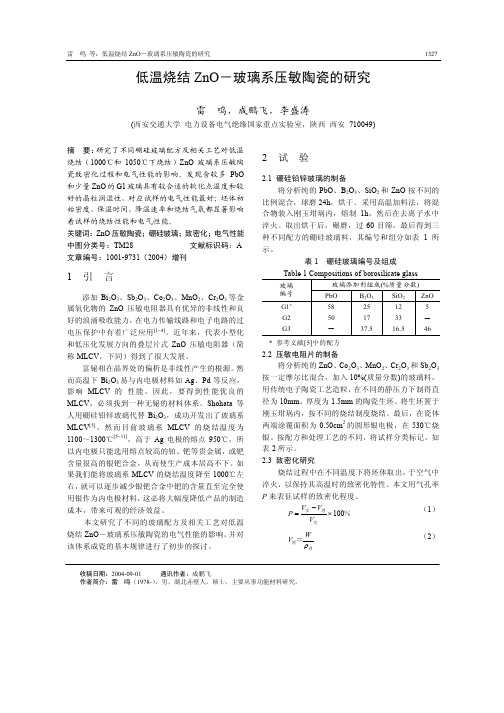
1327
低温烧结 ZnO-玻璃系压敏陶瓷的研究
∗
雷
鸣,成鹏飞,李盛涛
(西安交通大学 电力设备电气绝缘国家重点实验室,陕西 西安 710049) 摘 要: 研究了不同硼硅玻璃配方及相关工艺对低温
烧结(1000℃和 1050℃下烧结)ZnO 玻璃系压敏陶 瓷致密化过程和电气性能的影响。发现含较多 PbO 和少量 ZnO 的 G1 玻璃具有较合适的软化点温度和较 好的晶粒润湿性,对应试样的电气性能最好;坯体初 始密度、保温时间、降温速率和烧结气氛都显著影响 着试样的烧结性能和电气性能。 关键词:ZnO 压敏陶瓷;硼硅玻璃;致密化;电气性能 中图分类号:TM28 文章编号:1001-9731(2004)增刊 文献标识码:A
2+
雷 鸣 等:低温烧结 ZnO-玻璃系压敏陶瓷的研究
1329
晶粒润湿性差,使得试样 S2.1 晶粒尺寸最小,平均 击穿场强 EB 最大。然而,烧结过程中硼硅玻璃会在 晶界处重结晶,产生 5ZnO·2B2O3 和 2ZnO·SiO2 晶界 相[6,10]。因此,G2 玻璃可能会产生更多的 2ZnO·SiO2 相,使玻璃结晶度上升,从而引起晶界势垒高度 φB 和非线性指数 α 上升[10];这样就解释了尽管 G2 玻璃 润湿性不如 G1, 但 S2.1 的非线性并不明显差于 S1.1。 综上可见,G1 玻璃具有较为合适的软化点温度,因 此对应试样的晶粒较均匀,电性能较好。 表3 玻璃配方对试样电性能的影响 图 3 试样初始密度对最小气孔率的影响 Fig 3 Influence of green density on the minimal porosity 我们将初始密度为 3.18 g/cm3 的试样的致密化过 程延长至 1150℃,发现气孔率甚至上升至 15%以上。 这表明:当坯体的气孔率到达最小值时,瓷体内大部 分气孔都已成为闭气孔,此时若继续升高温度,瓷体 中低熔点物质挥发后将无法顺利排出, 导致瓷体内部 气孔率显著上升。 3.3 保温时间的影响 以试样 S1.6 为例, 在 1000℃时其烧成密度随保 温时间的变化如图 4。 Table 3 Influence of glass compositions on the samples’ performance
《ZnO及ZnO-石墨烯复合材料气敏性能研究》范文
《ZnO及ZnO-石墨烯复合材料气敏性能研究》篇一ZnO及ZnO-石墨烯复合材料气敏性能研究摘要:本文重点研究了氧化锌(ZnO)及其与石墨烯复合材料的气敏性能。
通过对比分析不同制备方法、材料结构以及其应用在气敏传感器上的表现,深入探讨了ZnO及其复合材料在气体检测领域的潜力和应用前景。
一、引言随着环境监测和工业安全需求的不断提高,气体传感器在诸多领域的应用日益广泛。
氧化锌(ZnO)作为一种重要的半导体材料,因其良好的气敏性能和制备工艺的简便性,在气体传感器领域具有重要地位。
近年来,石墨烯因其卓越的导电性能和大的比表面积,与ZnO结合形成的复合材料在气敏性能上展现出更优异的性能。
因此,对ZnO及ZnO/石墨烯复合材料的气敏性能研究具有重要意义。
二、ZnO及其基本气敏性能ZnO作为一种n型半导体材料,因其较高的电子迁移率和良好的化学稳定性,在气敏传感器中得到了广泛应用。
其气敏机制主要基于表面吸附和脱附过程引起的电阻变化。
然而,纯ZnO材料在灵敏度、响应速度以及稳定性等方面仍有待提高。
三、ZnO/石墨烯复合材料的制备及结构特点为进一步提高ZnO的气敏性能,研究人员将石墨烯与ZnO 结合,形成ZnO/石墨烯复合材料。
通过特定的制备方法,如溶液混合法、化学气相沉积法等,成功制备出具有不同比例的ZnO/石墨烯复合材料。
这种复合材料不仅具有ZnO的半导体特性,还因石墨烯的引入而提高了电子传输效率和比表面积,从而增强了气敏性能。
四、气敏性能研究及分析通过对ZnO及不同比例的ZnO/石墨烯复合材料进行气敏性能测试,我们发现:1. 复合材料较纯ZnO表现出更高的灵敏度和更快的响应速度。
2. 石墨烯的含量对复合材料的气敏性能有显著影响。
适量的石墨烯可以提高电子传输速率和吸附位点,从而提高灵敏度;但过多的石墨烯可能导致材料结构松散,反而降低气敏性能。
3. 不同气体对ZnO及ZnO/石墨烯复合材料的响应程度存在差异,这可能与气体的化学性质和材料的表面吸附能力有关。
ZnO_B_2O_3_P_2O_5系封接玻璃的研究
0
70
285
900
353
300
2.63
7.1
2
30
10
60
384
950
425
430
2.56
4.3
3
30
20
50
412
980
460
440
2.68
4.4
4
30
30
40
433
1050
480
453
2.74
4.7
5
30
40
30
பைடு நூலகம்406
1070
540
562
2.80
4.9
6
40
0
60
319
930
370
344
2.70
络中间离子掺杂在玻璃网络中。
2 实 验
本文实验用原料包括B2O3、ZnO、P2O5等,其 中B2O3用H3BO3引入,P2O5用HPO3引入,均为市售 化学纯试剂。根据前人研究结果,设计无铅磷酸盐 玻璃配方中各氧化物的组成范围为(mol%):ZnO 30-60;B2O3 0-40;P2O5 20-70。
图5 7#玻璃在不同pH值溶液中的失重率
4 结 论
·22·
(1)在ZnO-B2O3-P2O5玻璃结构中,B2O3和 P2O5为玻璃网络形成体,ZnO含量较低时可以参与 到玻璃网络结构中,提高玻璃的稳定性,但含量过 高时则对玻璃网络形成不利。ZnO含量是影响该玻 璃密度的主要因素,ZnO的含量增加,玻璃密度也 相应增大。
8.0
7
40
10
50
490
960
490
集成电路制造论文
离子注入掺杂对ZnO薄膜性能的影响The influence of ion implantation on the ZnO thin film姓名:郝秀秀西安电子科技大学摘要氧化锌(ZnO)是一种重要的宽禁带(室温下Eg--3.37eV)直接带隙半导体材料。
离子注入是将具有高功能的掺杂离子引入到半导体中的一种工艺.其目的是改变半导体的载流子浓度和导电类型.本论文是利用离子注入技术进行掺杂和热退火处理ZnO薄膜改性。
利用溶胶凝胶方法在石英玻璃衬底上制备了ZnO薄膜,将能量56 keV、剂量1×10"cm-2的Zn离子注入到薄膜中。
离子注入后,薄膜在500~900℃的氩气中退火,利用X射线衍射谱、光致发光谱和光吸收谱研究了离子注入和退火对ZnO薄膜结构和光学性质的影响。
结果显示:衍射峰在约700℃退火后得到恢复;当退火温度小于600℃时,吸收边随着退火温度的提高发生蓝移,超过600℃时,吸收边随着退火温度的提高发生红移。
关键词:ZnO薄膜;离子注入;退火温度;吸收;光致发光。
ABSTRACTZinc oxide (ZnO) is a kind of important wide forbidden band (Eg at room temperature-3.37 eV) direct bandgap semiconductor materials. Ion implantation iswill have high function into thedopingisemiconductor process. The aim is to change the charge carriers concentration and semiconductor conductive type.The present paper is using ion implantation technology and thermal annealing processing doped ZnO thin film modification. Using sol-gel method in quartz glass substrates gel preparation ZnO films, the energy 56 keV, dose 1 X 10 "cm-2 of Zn ion implantation to film. Ion implantation, film in 500 ~ 900 ℃ in the argon annealing, X-ray diffraction spectrum, the light spectrum and light absorption spectrum to send the ion implantation and annealing ZnO thin film on the influence of the structure and optical properties.The results showed that: about 700 ℃ in the diffraction peak after annealingrestoration; When the annealing temperature is less than 600 ℃, the temperature of the annealing edge with absorb blue to move, raise happen more than 600 ℃, the temperature of the edge with absorption annealing improve red shift occurred.Keywords: ZnO films; Ion implantation; Annealing temperature; Absorption; The light to shine.引言作为宽禁带半导体材料,ZnO近年来引起了广泛的研究兴趣。
最新的关于ZnO缺陷及其对光、电、磁性质影响的综述
Role of defects in tailoring structural,electrical and optical properties of ZnOSreetama Dutta a ,S.Chattopadhyay b ,A.Sarkar c ,Mahuya Chakrabarti d ,D.Sanyal d ,D.Jana a,*aDepartment of Physics,University of Calcutta,92Acharya Prafulla Chandra Road,Kolkata 700009,India bDepartment of Physics,Taki Government College,Taki 743429,India cDepartment of Physics,Bangabasi Morning College,19Rajkumar Chakraborty Sarani,Kolkata 700009,India dVariable Energy Cyclotron Centre (VECC),1/AF,Bidhannagar,Kolkata 700064,Indiaa r t i c l e i n f o Article history:Received 25March 2008Received in revised form 15July 2008Accepted 16July 2008a b s t r a c tIn this short topical review,a brief account of the evolution of defects due to controlled changes in polycrystalline zinc oxide has been presented.X-ray diffraction,Positron annihilation spectros-copy and optical absorption spectroscopy has been employed to understand various defective states of ZnO.Thermogravimetric analysis,room temperature resistivity and photoluminescence measurements (just mentioned)have been used to throw more light on this topic.A coherent scenario in the light of previous works in this field has been discussed.At the end discussion on the mag-netic studies on ZnO-based systems has been added in short.Ó2008Elsevier Ltd.All rights reserved.Contents 1.Introduction .........................................................................911.1.General........................................................................911.2.Defect physics and chemistry in ZnO................................................921.3.Some recent developments and the scope of this review................................932.Sample preparation,conditioning and scientific motivation...................................942.1.Heat treatment (annealing).......................................................942.2.Mechanical milling (ball-milling)ling and subsequent annealing ..................................................952.4.Ion-beam irradiation.............................................................953.Characterization techniques used and their specific importance in this study . (95)0079-6425/$-see front matter Ó2008Elsevier Ltd.All rights reserved.doi:10.1016/j.pmatsci.2008.07.002*Corresponding author.Tel.:+913323508386x413;fax:+913323509755.E-mail address:djphy@caluniv.ac.in (D.Jana).Progress in Materials Science 54(2009)89–136Contents lists available at ScienceDirectProgress in Materials Sciencej o u r n a l h o m e p a g e :w w w.e l s e v i e r.c o m /l o c a t e /p m a t s c i90S.Dutta et al./Progress in Materials Science54(2009)89–1363.1.Powder X-ray diffraction study (95)3.2.Measurement of resistivity (96)3.3.Positron annihilation spectroscopy(PAS) (96)3.3.1.Positron annihilation lifetime(PAL)measurement (97)3.3.2.Coincidence Doppler broadened positron annihilation radiation(CDBPAR)measurement (98)3.4.Thermogravimetric analysis(TGA) (99)3.5.Ultraviolet–visible(UV–Vis)absorption spectroscopy (99)4.Results and discussion (100)4.1.Strain evolution in ZnO as a consequence of changing defect structure (100)4.2.Positron annihilation spectroscopic investigation on ZnO samples (105)4.3.Study of optical properties of ZnO (111)4.3.1.Two important parameters for ZnO (111)4.3.2.General theory of absorption spectroscopy:band gap (113)4.3.3.Variation of band gap with crystallite size (118)4.3.4.Experimental results on band gap (120)4.3.5.Effect of disorder on electronic states (123)4.4.Short description of magnetic behavior of ZnO (130)5.Conclusions and new understandings (131)Note added in proof (132)Acknowledgments (132)References (133)Abbreviations1.Analog to digital conversion ADC2.Atomic superposition ATSUP3.Chemical vapor deposition CVD4.Coherent scattering region CSR5.Coincidence Doppler broadening of the annihilation radiation CDBAR6.Coincidence Doppler broadened electron–positron annihilation c-radiation CDBEPAR7.Coincidence Doppler broadening of positron annihilation radiation line shape CDBPARL8.Conduction band CB9.Density of states DOS10.Density functional theory DFT11.Electron density distribution EDD12.Electron momentum distribution EMD13.Electron paramagnetic resonance EPR14.Full width at half maxima FWHM15.Grain boundary GB16.High purity germanium HPGe17.Infra-red IR18.Local density approximation LDA19.Metal oxide chemical vapor deposition MOCVD20.Oxygen vacancy V O21.Oxygen antisite O Zn22.Photoluminescence PL23.Positron annihilation spectroscopy PAS24.Positron annihilation lifetime PAL25.Photomultiplier tube PMT26.Room temperature RT27.Shape parameter S-parameter28.Slow cool SL-CS.Dutta et al./Progress in Materials Science54(2009)89–1369129.Scanning tunneling microscopy STM30.Superconducting quantum interference device SQUID31.Thermogravimetric analysis TGA32.Topologicalfilaments TF33.Time resolution TR34.Ultraviolet–visible UV–Vis35.Valence band VB36.Variable range hopping VRH37.Williamson–Hall plot W–H plot38.Wing parameter W-parameter39.X-ray diffraction XRD40.Zinc vacancy V Zn41.Zinc oxide ZnO1.Introduction1.1.GeneralZnO has been discovered and rediscovered many times.Thanks to its extreme complexity of defect physics and chemistry,which probably opens the scope of being rediscovered time and again[1–4].In fact, this limitation has become advantageous from materials science point of view.ZnO has become one of the benchmark materials to test several theoretical models in condensed matter physics[5–11].On the other hand,infinite avenues or possibilities exist for innovative tuning of the material according to the techno-logical need.This is reflected in the increasing interest and publications on ZnO related research[1,12].ZnO is thought to be one of the most promising candidates for applications in spintronic and opto-electronic devices.It is being used frequently in solar cells,transparent thinfilm transistors,ultraviolet (UV)photodetectors,light emitting diodes(LEDs),piezo-electric devices[1,2,13–17].Particularly nanocrystals of ZnO show some fascinating properties like room temperature(RT)lasing in UV and visible region,magnetic hysteresis above the ambient and selective sensing of gases[18–20].ZnO has a direct band gap of$3.3eV at RT and exciton binding energy$60meV(much higher than $21meV in GaN)[21].Such remarkable property makes it a lucrative material for RT UV lasing de-vices.Most frequently,ZnO shows n-type conductivity,which arises due to one or more of its native defects[9].Realizing p-type ZnO easily is still debated[22–26]and this remains as a disadvantageous factor for its non-linear device applications[27].Most modern techniques of crystal growth make it possible to grow high quality large size ZnO crystals and wafers[28].It has remarkable consequences on wide industrial use of ZnO.But quite interestingly,polycrystalline,nanocrystalline or a typical defective ZnO material shows remarkably new properties[13,18,29–37],which bear importance both from theoretical and technological as-pects.Such so-called low quality(not in terms of purity)ZnO offers moreflexibility to be exploited in device applications and that is due to the abundance of various defect species in such system [38].They can be produced with lower cost and by relatively easier techniques[39–46].In this way,polycrystalline or nanocrystalline ZnO have become even more attractive.In its own right‘‘Defects in ZnO”has,thus,become one of the most discussed issues in condensed matter physics and materials science at present.A delicate balance of various defects in ZnO,gives rise to fundamentally new and newer material characteristics[47–50].At this stage,efforts continue in the direction to achieve an effective defect management in this material,with intrinsic or artificially doped defects.Defect characterization techniques,thus,play an important role in thisfield of research.Each of these techniques has some advantages as well as some limitations.For example,positron annihilation spectroscopy(PAS)[51]efficiently probes vacancy-type defects in a material,whereas,Rutherford back scattering(RBS)technique[52]is more sensitive to interstitial-type defects.X-ray diffraction(XRD) technique is extremely important not only to check the structural purity but also to identify pointdefects,extended defects and dislocation-related disorder [53,54].Results of temperature-dependent Hall (TDH)effect study bears information regarding the concentration,mobility and the thermal activa-tion energy of the free carriers in the system [55].The deep level transient spectroscopy (DLTS)detects the deep trap (0.15–0.8eV from one of the band edges)states in the band gap [51].Such states indeed arise from defects and for wide band gap materials,such as ZnO,this technique has particular impor-tance [56].Photoluminescence (PL)and optical absorption measurements are also extremely helpful for characterization of ZnO material.The optical band gap of the material as well as the possible radiative and non-radiative centers can be understood from these techniques [57–60].Raman spectroscopy is a sensitive tool to probe oxygen vacancies in ZnO [61].Electron paramagnetic resonance (EPR)spectros-copy makes use of the resonant absorption of the electromagnetic radiation by unpaired electrons in the material placed under a magnetic field.It is extremely important for defect probing in ZnO,however,the assignment of EPR signal with a particular defect in ZnO has often been debated [62].X-ray photoelec-tron spectroscopy (XPS)scans the compositional disorder in the sample.Electron energy loss spectros-copy (EELS)is an important technique to probe the complex dielectric function and thereby the refractive index in ZnO [63].Techniques based on electron microscopy are also playing an important role in characterizing ZnO nanosystems [64].Due to extreme complexity of the ZnO defect structure,it is always beneficial [55,56,65,66]to use two or more techniques simultaneously.Results of several tech-niques,employed at a time,should bear some similarities and differences as well.A comparative analysis and understanding of these aspects,still at large,would be helpful to choose suitable characterization techniques for defect probing in ZnO.So,understanding on the theoretical aspects of the role of defects in ZnO,methodology of controlled defect creation in this system and proper choice of characterization techniques,can meet the challenge of purposeful defect management in ZnO.In this review,we shall focus our discussion on intrinsic or native defects in ZnO.1.2.Defect physics and chemistry in ZnOThe concentration of any point defect in a lattice depends on the formation energy through Boltz-mann factor.If there are N atoms,the equilibrium defect concentration n is given byn N Àn ¼exp ÀE fk B T!ð1ÞHere E f is the formation energy,k B the Boltzmann constant and T being the temperature.This equation can be derived by considering free energy model of the system without taking the defect-defect inter-action.In the limit n (N ,the above equation reduces to a simple formn ffiN exp ÀE fB !ð2ÞThis equation indicates two important facts:(i)The equilibrium vacancy concentration decreases with increase of temperature.(ii)Defects having high formation energies will occur in low concentrations.In all these simple-minded calculations,the important contributions from formation volume and formation entropy have not been taken into consideration.The formation energies and the electronic structure of native defects in ZnO have been investigated from first principle pseudopotential method [67,68].The total energy has been calculated through supercell approach.This is required as we are interested to energetics of isolated point defects in an infinite crystal.The infinite limit is attained via this super-cell method.The formation energy for a defect in charge state q is computed via the relationE for ðq Þ¼E T ðq ÞÀn Zn m Zn Àn O m O þqE Fð3Þwhere E T (q )is the total energy of the supercell with a defect of charge state q ,n Zn (n O )is the number of zinc (oxygen)atoms in the supercell,l Zn (l O )is the relevant atomic chemical potential,and E F is the Fermi energy.92S.Dutta et al./Progress in Materials Science 54(2009)89–136S.Dutta et al./Progress in Materials Science54(2009)89–13693Of course,we have the constraint equations for the atomic chemical potentials lþl O¼l ZnOðbulkÞð4ÞZnIt is seen that the Fermi energy depends on the concentration of native defects as well as impuri-ties.In ZnO structure,there are two ways one can place an atom interstitially in the structure–one is in an octahedral site and the other is in a tetrahedral one.It was noticed that the zinc vacancy exhibits the lowest formation energy among the defects associated with oxygen excess.Even in the oxygen rich limit,the Zn vacancy has the lowest formation energy.The formation energy of a typical point defect depends on environment such as growth or anneal-ing conditions[9].Thefinite temperature thermodynamical stability condition for bulk ZnO is written aslþl O¼D H fðZnOÞð5ÞZnwhere D H f(ZnO)is the enthalpy formation of bulk ZnO and for a stable compound,this enthalpy must be negative.The calculated value(À3.5eV)of D H f(ZnO)matches well with experimental value of À3.6eV[62].For n-type materials[6],the oxygen vacancy should be dominant among the donor type defects. The electronic structure of oxygen vacancy reveals that the state is likely to appear near the top of the valence band(VB)maximum.For zinc interstitials,the defect induced state shows resonance with the conduction band(CB).This observation can explain the n-type conductivity of undoped ZnO.The complex defect physics of ZnO has been investigated thoroughly by Zhang et al.[8]to explain the intrinsic doping asymmetry.The microscopic analysis establishes that(i)ZnO is n-type at Zn rich conditions,(ii)ZnO cannot be made p-type via native defects and(iii)electron–hole recombination at the oxygen vacancy as the main source of green luminescence.Thefirst principle calculations of the energy[5]related to defects show that both the Zn and O vacancies are the relevant defects in ZnO.The computational advantage in this work is better than the previous one for identifying the various defects present in ZnO.However,because of the local den-sity approximation(LDA)in their calculations,the band gaps as well as the defect levels are suffi-ciently lower than the experimental values.In spite of this,the mechanism leading to green luminescence centered on2.4and2.5eV in ZnO may be explained via the energies of the defect levels. The luminescence is due to the transition of electrons in the CB to a deep acceptor level of Zn vacancy.To overcome the underestimated band gap problem in LDA approaches recently Janotti and Van de Walle[62]have performed DFT calculations in LDA+U approach.Theyfind that the oxygen vacancies are deep donors while Zn interstitials are shallow donors.The n-type conductivity of ZnO in this framework can be explained via the unintentional incorporation of donor impurities.From their tran-sition state theory of defect,the typical barrier height of oxygen vacancy(V O)was found as2.36eV with annealing temperature909K.1.3.Some recent developments and the scope of this reviewThe vastness of ZnO research makes it impossible to note all the developments in thisfield.The results from different groups have often found to be contradictory.A representative list of the recent works is being described here.Fortunately,intrinsic vacancy type defects are most abundant in ZnO [5]and PAS has particular sensitivity to such defects.[55,66,69–74].Nature of PL and the possible de-fects/defect complexes present in ZnO have been investigated through PAS by Koida et al.[58]and Zubiaga et al.[75].The optical absorption in ZnO has been correlated with defects by Selim et al.[76]and de la Cruz et al.[77].In a highly cited work by Vanheusden et al.[59],the optical absorption and PL in ZnO powder has been investigated and a correlation with green luminescence($510nm) and V O s(oxygen vacancies)has been drawn with the help of EPR results.However,their conclusion has recently been contradicted by Janotti and Van de Walle[62].The later group favored for V Zn as the possible candidate for visible luminescence in ZnO.Passivation of the elctronic states of the V O s have been attempted by S doping[78],F doping[79],or simply by aging[80].The dependence of the optical absorption with high pressure[81],with Mg doping[80],with embedded ZnO nanoclusters in ZnO host matrix[82]and with various other defects and disorder[6,60,77,83–86]have also been94S.Dutta et al./Progress in Materials Science54(2009)89–136investigated.In an interesting report Watanabe et al.[87]revealed negative thermal quenching behav-ior of ZnO grown by radical source molecular beam epitaxy(RS-MBE)technique.The possible effect of the grain boundary defects on PL in polycryatalline ZnO have been investigated by Ong et al.[31],Ra-doi et al.[88],Shalish et al.[89]and by Matsumoto et al.[90].In an important study,Tiwari et al.[91]have reported a transition(in differently heat treated ZnO) from band gap insulator to Anderson localized insulator by measuring temperature dependence of resistivity and thermopower.Modification of resistive nature of ZnO with doping has also been inves-tigated by Bhosle et al.[92],Kim et al.[93]and Han et al.[94].In last few years,several new reports have come up which triggered aspirations for the large scale technological use of ZnO.Thefirst one of this kind is the p-type ZnO fabrication,which is important to achieve non-linear devices like diodes or transistors.Consolidated efforts are being paid through doping with P or As or N[22–24,26,27,95]or by means of co-doping of two dopants[96].The second one is the report of room temperature UV–Vis lasing in polycrystalline ZnO[19,29,30,97,98].The tuning of grain boundary defects in ZnO is very much important in this context[31].The third one is the achievement of ZnO-based dilute magnetic semiconductors(DMS).The origin of such magnetic phenomena in doped or undoped ZnO system is still a mater of intense debate[2,11,18,37,47,99–108].However,it has been conjectured that n-type conduction destroys the ferromagnetic exchange interaction[101]and that is why low temperature processing of such materials to reduce V O are very much important[47,102,105].However,there exist reports[18,107]where the idea of doping induced ferromagnetic behavior in ZnO has been contested. Finally,it should be noted at this point that in most of the reports mentioned above the intrinsic or native defects play crucial role to determine the material properties of ZnO.There exist a good number of reviews[2–4,13,16,17,64,108]in thefield of ZnO research.A general review on application of PAS on II–VI semiconductors can be found in Ref.[51].However,our review has been written from a different angle and it is more topic specific which,in general,is‘‘role of native defects in ZnO”.In this Section1,theoretical and experimental aspect of the ZnO research in recent past has been briefly outlined.In Section2,different techniques of ZnO sample conditioning has been described with their specific relevance.In Section3,a somewhat detailed description of the character-ization techniques has been given to make the discussion of the results in Section4more understand-able.In Section5,interesting part of the results has been briefly sketched to trigger new ideas and experiments.2.Sample preparation,conditioning and scientific motivation2.1.Heat treatment(annealing)Annealing at elevated temperatures is,probably,the most efficient technique to tailor the defective state of ZnO.Suitable choice of temperature[66,109–111],time[112,113]and annealing ambient environment[76,111,114],rate of heating and cooling of annealing[22,115,116]has been proved ben-eficial to monitor material properties in a controllable fashion.However,an effective control over thermally generated unwanted defects could not be established till date.In the present study,as-sup-plied polycrystalline ZnO powder(purity99.9%from Sigma–Aldrich,Germany)have been palletized ($1mm thickness and10mm diameter)and annealed in a programmable quartz tube furnace at 200°C,300°C,400°C,600°C,800°C,and1000°C for18h followed by slow cooling(30°C/h)in air. Another set of thermally-annealed samples(300°C,400°C,600°C,800°C,900°C,and1000°C)has been prepared in the above process with furnace cooling only varying the annealing time(4h).One part of this4-h annealed sample has been rapidly quenched from800°C to liquid nitrogen tempera-ture(À196°C).In this way it has been attempted to freeze the high temperature disordered state of the material[117,118].2.2.Mechanical milling(ball-milling)The mechanical milling technique(popularly known as ball-milling)[33,44,88,119,120]is a simple but effective method to produce large quantity of nanomaterials.This technique offers a negligibleS.Dutta et al./Progress in Materials Science54(2009)89–13695little contamination during production of the material,which is important for industrial use.However, during the milling huge amount of defects is induced in the materials those cannot be well regulated [121].The particle size(CSR size,detailed in Section3.1)distribution has been found to be very high in milled material.At the same time,the lower limit of the particle size is set by the surface roughness of the container and milling balls.In the present study,nanocrystalline ZnO samples have been prepared by ball milling as-supplied ZnO powders in a Fritsch Pulverisette6planetary ball mill grinder.The milling time has been varied from1h to32h to achieve nanocrystalline ZnO of varying average grain size(ball:mass ratio10:1).The milled sample will be termed as batch I.Another set of samples has been prepared in a same process(ball:mass=9:1)with relatively small time interval(10,20,40, 80,160,320,640,and1280min).These samples will be termed as batch II.ling and subsequent annealingIt is of scientific interest to monitor the thermal evolution of defects in an as-milled material with high concentration of defects and disorder.In the present work,the same ZnO powder mentioned above has been ball-milled(ball:mass=35:1)for3h and then annealed at different temperatures (in the range210–1200°C)for4h followed by slow cooling(30°C/h)in air.The milled and un-an-nealed sample will be termed as Nano-ZnO-III.For a comparative study,the particular800°C annealed sample has been quenched to liquid nitrogen.2.4.Ion-beam irradiationZnO is famous for its unique radiation hardness,which suits for applications in outer space [122,123].Ion-beam irradiation has been performed at room temperature on350°C and500°C an-nealed ZnO samples to study the defects induced by ion-beam irradiation on the particular system. These annealed samples have been irradiated by100MeV Si8+beam with differentfluences (1Â1013,6Â1013,1Â1014ions/cm2)at15UD pelletron accelerator of Inter University Accelerator Centre(IUAC),New Delhi.In the present ion beam irradiation experiment focused beam area is 1cm2and the beam current has been set to1pnA(particle nanoAmpere).3.Characterization techniques used and their specific importance in this study3.1.Powder X-ray diffraction studyThe powder XRD measurements have been performed on all the ZnO samples to check the phase purity of all the samples.The spectra have been recorded at Saha Institute of Nuclear Physics(SINP), Kolkata,by a Philips PW1710automatic diffractometer with Cu K a radiation(wave length of the radi-ation,k=1.54Å).Data have been collected in the range(2h)20–70°with a step size of0.02°.The grain sizes of the powdered samples have been calculated using Scherrer formula[124].b P¼K k=D hkl cos hð6Þwhere D hkl is the average grain size,K the shape factor(taken as0.9),k is the X-ray wavelength,b P is the full width at half maximum(FWHM)intensity(here101peak of the ZnO spectrumfitted with a Gaussian)and h is the Bragg angle.A particular peak in the X-ray diffractogram is generated due to coherent scattering of X-rays from a particular lattice planes indexed by respective hkl values.The size of the domain(or column)of the coherently scattering region(CSR)in direction parallel to a diffraction plane is related with the inverse of FWHM of the respective diffraction peak[125,126].An infinitely large domain(in single crystals)contributing coherently to that respective XRD peak will produce a line only.Butfinite resolution of the instrument itself and other factors[127]will broaden the peak. Standard method[125]to deduct the contribution of instrumental broadening in b P has been taken into account in our study also.The presence of defects and disorder(like point defects,faults,disloca-tions,grain boundaries,etc.)in the sample essentially hampers the coherent scattering and thus the domain size is truncated.If the disorder is not large enough(not turned the sample to an amorphous96S.Dutta et al./Progress in Materials Science54(2009)89–136one)to destroy the coherency completely,coherent scattering from different domains will produce diffraction peaks at different positions but close to that of the reference position of a single crystal of the same material.Naturally,in polycrystalline samples with sufficiently low CSR size(popularly known as grain or particle size)the characteristic XRD peaks of the sample get broadened compared to those of its single crystal.The overall broadening is determined by the volume-weighted sum of the peaks generated from each domain[54].So such broadened XRD peaks carry information regarding the average CSR size and also their size distribution.However,the situation becomes complex when there exist inhomogeneously distributed defective sites.This situation often occurs in polycrystalline (and also in nanocrystalline)materials where grain interior is relatively defect free(or contain scat-tered small size point defects)and the grain boundary consisting of high-density defect clusters [53,54].Analysis of peak broadening has been done here assuming a simplified picture of the actual one[128].It is thought that overall broadening of a peak can be divided into two parts–one part is due tofinite size of the CSR(size broadening)and the other part is due to random displacements of atoms from their original positions near the defect rich grain boundaries.Such local distortion of the lattice generates strain in the lattice and its contribution to peak broadening is known as strain broadening.It is not very unambiguous to separate two contributions but their qualitative features can be estimated through constructing Williamson–Hall(W–H)plot with different peaks[129].Con-sidering strain effect,one can easily rewrite the equation for W–H plot asb¼K k=D hkl cos hþ2e tan hð7Þwhere microstrain parameter e is=|D D hkl/D hkl|.To note,the strain value thus obtained is indeed the root mean square(r.m.s.)value over a length scale of the grain or CSR size assuming that the strain exist in the system,whatever may be its type,is isotropic in nature.If some anisotropic strain occurs in system due to specific reason of generation of particular defect type,as we will see later,the con-struction of W–H plot may not be purposeful due to data scattering[130].To construct a W–H plot,one needs the integral breadth(b=A/I o,where A being the peak area and I o the height of the observed line profile)of different X-ray peaks,corrected for instrumental broadening andfitted with a Lorentzian profile.In this method,it is assumed that the peak broad-ening due to size effect does not depend on the reflection order;whereas strain depends on it(It will be easier to understand if the equation is written in reciprocal space[21]).Therefore,using several peaks of the same family,it is possible to separate these two contributions.In the present study, (100),(002),(101),(102),(110),(103),(112)peaks have been used for W–H plot.As we can sep-arate the grain size and strain part,the general tendency of estimated grain or CSR sizes calculated from the W–H plot are higher than those obtained from Scherrer’s formula.However,complex sys-tems with variety of defect species,particularly in nanomaterials,the application of Scherrer’s for-mula provides a better description of the overall defective nature of the system.Without any simplified assumption,it considers that XRD line broadening as a combined effect of defects and dis-order of all types.3.2.Measurement of resistivityVariation of resistivity in ZnO with thermodynamic variables such as pressure[33]and tempera-ture[91,131]or with doping[132],irradiationfluence[133]and annealing conditions[109]bears valuable information regarding the defects present in the system and their role on carrier conduction. In this study,monitoring of room temperature resistivity with annealing temperature has been carried out for18-h annealed sample only.Resistivity has been measured by usual four probe technique with silver paint contacts.Keithley2182nanovoltmeter and2400constant current sources have been used. Due to very high resistances of the unannealed,200°C and300°C-annealed samples,the resistivity has been measured by two-probe Keithley6514electrometer.3.3.Positron annihilation spectroscopy(PAS)Positron annihilation lifetime(PAL)measurement technique and coincidence Doppler broadening of the electron–positron annihilation radiation(CDBEPAR)measurement technique,are two nonde-。
- 1、下载文档前请自行甄别文档内容的完整性,平台不提供额外的编辑、内容补充、找答案等附加服务。
- 2、"仅部分预览"的文档,不可在线预览部分如存在完整性等问题,可反馈申请退款(可完整预览的文档不适用该条件!)。
- 3、如文档侵犯您的权益,请联系客服反馈,我们会尽快为您处理(人工客服工作时间:9:00-18:30)。
编号毕业设计(论文)题目ZnO对低硅高硼低介电常数玻璃结构和失透行为的影响二级学院材料科学与工程专业材料科学与工程班级 110090303学生姓名豆兴春学号 11009030305指导教师田中青职称教授时间 2014年6月目录摘要 (Ⅰ)Abstract (Ⅱ)第一章前言 (1)1.1玻璃纤维和低介电玻纤 (1)1.2 低介电常数 (1)1.3 玻璃失透 (3)1.4 玻璃析晶 (3)1.5 玻璃分相 (4)1.6 本文研究内容及意义 (5)第二章实验过程及方法 (7)2.1 实验材料及设备 (7)2.2 实验过程及方法 (7)2.2.1 原料制备 (7)2.2.2 玻璃的熔制 (8)2.2.3 退火 (8)2.2.4 红外光谱 (8)2.2.5 示差扫描量热法 (9)2.2.6 热处理 (10)2.2.7 玻璃密度的测定 (10)2.2.8 X射线衍射 (11)2.2.9 扫描电镜 (11)第三章实验结果与分析 (13)3.1 红外光谱分析 (13)3.2示差热分析 (14)3.3 热处理分析 (15)3.4 玻璃密度分析 (16)3.5 X射线衍射分析 (17)3.6 扫描电镜分析 (20)第四章结论 (21)致谢 (22)参考文献 (23)文献综述 (25)摘要低介电玻璃是一种特殊玻璃,具有密度低、介电常数低、介质损耗低、介电性能受温度等特点,其产品可应用于国防领域和高精尖端民用领域。
ZnO对低介电玻璃的结构和失透行为都有一定的影响。
因此,本文通过改变ZnO的含量熔制出不同的玻璃。
采用XRD、IR、SEM等方法研究玻璃的结构,析晶以及分相程度。
主要的研究结果如下:(1)随着ZnO的增加,非桥氧振动增强,导致玻璃分相。
(2)在同一温度下,随着ZnO含量的增加,玻璃越来越容易失透。
(3)随着ZnO含量的增加,玻璃的密度逐渐越大。
(4)当ZnO含量为9%时,析出的物相为Al5(BO3)O6;当ZnO含量为12%时,析出的物相为Al2ZnO4。
关键词:ZnO 低介电玻璃玻璃的结构玻璃析晶玻璃分相AbstractLow dieletric glass is a special glass,it has a lot of advantages,such as low density, low dielectric constant and low dielectric loss, the product can be used in the fields of national defense and sophisticated civil field.ZnO for low dielectric glass structure and devitrification behavior has a certain effect.Therefore,this paper according to change the content of ZnO to founding to diferent glasses.Research the structure of glass,crystallization,and phase separation by XRD,IR,SEM.The following is the main results:(1)With the increase of ZnO,the vibration of non bridging oxygen becomes strengthen,lead to glass phase separation.(2)At the same temperature,with the increase of ZnO content,glass devitrification increasing easily.(3)With the increase of ZnO content,the density of the glass becomes enlarge.(4)When the content of ZnO is 9%,precipitated phase is Al5(BO3)O6;when the content of ZnO is 12%,precipitated phase is Al2ZnO4.Key words:ZnO the low dielectric glass the glass structure glass crystallization glass phase separation第一章前言1.1玻璃纤维玻璃纤维是一种性能优异的无机非金属材料,种类繁多,优点是绝缘性好、耐热性强、抗腐蚀性好,机械强度高,但缺点是性脆,耐磨性较差。
玻璃一般做为质硬易碎物体,并不适于作为结构用材,但若抽成丝后,则其强度大为增加且具有柔软性,故配合树脂赋予形状以后终于可以成为优良之结构用材。
玻璃纤维是以玻璃球或废旧玻璃为原料经高温熔制、拉丝、络纱、织布等工艺制造成的,其单丝的直径为几个微米到二十几个微米,相当于一根头发丝的1/20-1/5 ,每束纤维原丝都由数百根甚至上千根单丝组成。
玻璃纤维随其直径变小其强度增高[1]。
玻璃纤维比有机纤维耐温高,不燃,抗腐,隔热、隔音性好(特别是玻璃棉),抗拉强度高,电绝缘性好(如无碱玻璃纤维)。
但性脆,耐磨性较差。
玻璃纤维按形态和长度,可分为连续纤维、定长纤维和玻璃棉;按玻璃成分,可分为无碱、耐化学、高碱、中碱、高强度、高弹性模量和耐碱(抗碱)玻璃纤维等。
玻璃纤维主要用作电绝缘材料,工业过滤材料,防腐、防潮、隔热、隔音、减震材料。
还可作为增强材料,用来制造增强塑料或增强橡胶、增强石膏和增强水泥等制品。
用有机材料被覆玻璃纤维可提高其柔韧性,用以制成包装布、窗纱、贴墙布、覆盖布、防护服和绝电、隔音材料。
玻璃纤维是非常好的金属材料替代材料,随着市场经济的迅速发展,玻璃纤维成为建筑、交通、电子、电气、化工、冶金、环境保护、国防等行业必不可少的原材料。
由于在多个领域得到广泛应用,因此,玻璃纤维日益受到人们的重视。
不同类型的玻璃纤维因性能的差异而有不同的用途。
玻璃类型决定着玻璃纤维的一些主要电学性能,且在很大程度上决定着应用范围。
低玻璃纤维由于其电绝缘性能好、介电损耗低、介电性能受温度、频率等变化影响小,耐高温,织物后加工性能好等特点,而被广泛应用于当今的电子工业[2]。
因此,很有必要对低介电常数的玻璃进行一些简单的介绍。
1.2低介电常数和低介电玻纤在介绍低介电常数之前,简单的介绍一下介电常数。
介质在外加电场时会产生感应电荷而削弱电场(真空中)与最终介质中电场的比值就叫做介电常数,又称诱电率,通常以字母 表示,单位为法/米,表示电介质在电场中贮存静电能的相对能力。
它是表征绝缘能力的一个系数,介电常数越小,绝缘性越好,反之则越差,会使信号的传输速率变慢。
顾名思义,为了获得低介电常数的材料,必然在介电常数的基础上进行加工,使介电常数变得更低。
压层板的低介电可以从树脂和玻纤布两方面来实现,一方面可以使用氰酸酯,苯乙烯马来酸酐,PPO/APPE,以及其它改性热固性塑料等低级分子结构的材料来产生低介电常数[3]。
低介电常数材料分为有机和无机低介电常数材料,含氟低介电常数材料主要应用于电子行业,可以降低集成电路的漏电电流、导线之间的电容效应和集成电路发热等。
李志进、陈奇等人经过实验发现,随着ZnO摩尔分数的增加,材料的介电性能有所下降。
而随着ZnO含量的增加,玻璃失透越来越困难[4]。
低介电玻璃,用于生产介电强度好的低介电玻璃纤维。
其介电常数和损耗均较低,通常用于透波复合材料的增强基材以及大容量高速印刷线路板上。
近年来对印刷线路板容量寿命信号传输速度等提出更高要求,需较低的介电常数和损耗更高的工艺和应用稳定性,为此在已有的低介电玻璃纤维基础上,开发了D3、NE等低介电玻璃纤维。
低介电玻璃纤维可在现有的覆铜板制造工艺装备条件下生产,在简易生产工艺设计、降低成本、改良覆铜板研究设计、实现产品性能稳定方面均有突破性进步。
由此可见,低介电玻璃纤维是高密度多层互连印制电路板低成本化生产的关键原材料,解决了制约玻璃纤维布作为高密度多层印制电路板增强材料的技术瓶颈[5]。
为了降低玻璃的介电常数与介电损耗,许多研究者都会在组成中加入较高含量的SiO2、B2O3、Al2O3。
王中俭等人指出这是因为这类氧化物属于玻璃网络的形成体和中间体,结合能高,在外电场作用下不易产生极化,所以表现出较低的介电常数和介电损耗,同时还可以抑制玻璃析晶。
而碱金属离子与网络联系较弱,在外电场作用下容易迁移和极化,不但会增加玻璃的介电常数,还会降低它的电绝缘性,增加介电损耗,因此,在低介电常数玻璃纤维中很少引入.这一组成特点,决定了这类玻璃会有比较高的熔制温度和拉丝作业温度.降低玻璃中Al2O3含量,同时适当增加SiO2、TiO2或CaO,可以较好地兼顾玻璃的介电性能,并使玻璃的工艺参数满足工业生产的要求[6]。
1.3玻璃失透玻璃失透是指玻璃介质内部由于微小区域的不均匀而失去透明性。
玻璃的失透对玻璃是否能稳定地拉成玻璃纤维有决定性的影响,特别是玻璃的析晶上限温度。
玻璃的析晶上限温度至少要低于玻璃拉丝温度40~50 ℃以上,一般需低80 ℃以上,才能保证在拉丝作业时不受析晶及分相问题的影响。
均匀的玻璃态物质在一定温度范围内有可能分成两种互不溶解(或部分溶解)的液相,由于两者的折射率不一致,因光散射而形成乳白或浑浊。
因此对于光学玻璃来说,失透是必须防止的缺陷之一。
玻璃失透的原因一般可分为两种,即析晶和分相。
1.4玻璃析晶玻璃析晶指由于玻璃的内能较同组成的晶体高,玻璃处于介稳状态,在一定条件下存在着自发地析出晶体的倾向,这种出现晶体的现象叫作析晶。
一般从玻璃态中出现析晶,是在黏度为310Pa·s左右的温度范围(该10~5玻璃系统液相线温度以下)内进行的。
根据塔曼理论,析晶主要决定于晶核形成速率、晶核成长速度以及熔体的黏度,同时与玻璃液在该温度下的保温时间有关。
晶核形成速率是指在一定温度下在单位时间内单位容积中所形成的晶核数目(个)。
晶数/min)。
晶体成长速度是指在单位时间内晶体增长的直线长度(min/m核形成的最大速率和长大的最大速度分别在两个不同的温度范围内出现,只有在两者都较大的温度下最易析晶。
析晶是普遍现象,在相界、晶界或基质的结构缺陷等不均匀部位容易产生晶核。
这里的相界一般包括容器壁、气泡、杂质颗粒或添加物等与基质之间的界面,由于分栩而产生的界面,以及空气与基质的界面(即表面)等。
在符合温度和相界的条件下,生成晶核,在适宜晶核生长的黏度和温度条件下晶体生长,这些条件在任何熔窑内都是存在的。