飞思卡尔freescale代理
NXP恩智浦 Freescale飞思卡尔后你需要知道的十件事

NXP恩智浦Freescale飞思卡尔后你需要知道的十件事这两年,半导体行业似乎进入了多事之秋,收购战此起彼伏。
就在今年短短的3个月里,半导体行业并/收购案有:Avago Technologies 以6 亿美金价格收购无线网络公司Emulex Corp ELX.O,Maxlinear以2.87亿美元收购Entropic Communications,Lattice半导体则将以6亿美元价格收购Silicon Image。
3月初,恩智浦(NXP)以约118亿美元的价格并购飞思卡尔(Freescale),合并后的企业价值将超过400亿美元。
大公司的收购往往错综复杂,他们也有自己难以取舍的地方,有经济、情感、形象等多方面的考量。
这次并购会对恩智浦和飞思卡尔各自的产品、目标行业、半导体产业以及竞争对手带来哪些影响呢?我们目前还不能得到准确答案,但是希望能从对两家公司的十大对比中,让你看出一些端倪。
1.优势产品恩智浦微控制器、射频、传感器、无线(NFC)、模拟及电源。
杀手锏:NFC、智能卡IC。
飞思卡尔MCU&通信处理器、模拟技术与电源管理、射频、无线连接、传感器、软件和开发工具。
杀手锏:MCU&通信处理器(ARM MCU、ARM 应用处理器、QorIQ多核处理器、Power处理器、DSP)。
恩智浦+ 飞思卡尔不难发现,这两家的产品互补性很强,一个擅长连接,一个擅长处理和控制连接及其带来的数据。
恩智浦和飞思卡尔的专利数都约为10 000,可以从一个侧面反映他们的势均力敌。
而下面的专利“地图”,会让你直接感受到他们各自的强项。
图1 恩智浦与飞思卡尔的专利“地图” 在宣布合并交易时,恩智浦表示将出售自家高性能RF产品部门以避免主管机关审查问题,其实是因为NXP将保留原属于飞思卡尔、技术实力更强的RF部门,而不是他们自己的。
如果两家公司的RF业务合并,将有垄断全球高性能RF市场之虞,美国与欧洲的反垄断机构以及中国的商务部将审查这项合并交易。
Freescale 数字微处理器用户指南说明书

MPC5606S-DEMO-V2Freescale Semiconductor User’s GuideDocument Number:MPC5606SDEMOUGRev. 0, 10/2010 Contents1OverviewThe MPC56xxS family is the latest generation of 32-bit Power Architecture microcontrollers (MCUs) that address color thin-film transistor (TFT) displays in automotive instrument cluster applications. It offers a cost-effective entry-level instrument cluster solution with the ability to scale your designs to fit your performance needs.1.1Specific MPC5606S KeyFeatures•e200 32-bit Book E compliant CPU corecomplex built on Power Architecture technology •Display Control Unit (DCU) for direct drive of TFT displays up to WQVGA resolution •Stepper motor drivers (for driving up to six instrumentation gauges)•40 x 4 segment LCD display driver 1Overview . . . . . . . . . . . . . . . . . . . . . . . . . . . . . . . . . . . . . 1 2Power . . . . . . . . . . . . . . . . . . . . . . . . . . . . . . . . . . . . . . . 3 3Video. . . . . . . . . . . . . . . . . . . . . . . . . . . . . . . . . . . . . . . . 4 4Input/Output. . . . . . . . . . . . . . . . . . . . . . . . . . . . . . . . . . . 5 5Memory . . . . . . . . . . . . . . . . . . . . . . . . . . . . . . . . . . . . . . 7 6Communications . . . . . . . . . . . . . . . . . . . . . . . . . . . . . . . 7 7Debug . . . . . . . . . . . . . . . . . . . . . . . . . . . . . . . . . . . . . . . 9 8Sound . . . . . . . . . . . . . . . . . . . . . . . . . . . . . . . . . . . . . . . 9 9Initialization Code . . . . . . . . . . . . . . . . . . . . . . . . . . . . . . 9MPC5606S-DEMO-V2 User Guide by:Ioseph MartinezFreescale Applications EngineerTlaquepaque, JaliscoOverview• 1 MB on-chip flash with separate 64 k Data Flash for the EEPROM Emulation•48 KB on-chip SRAM with ECC•160 KB on-chip graphics SRAM (no ECC)•Parallel Data Interface (PDI) for digital video input•Sound generation and playback using PWM channels and DMA•QuadSPI Serial Flash ControllerThe MPC5606S-DEMO-V2 allows testing most of the MPC5606S MCUs features, especially graphics. The following block diagram shows the functionality and architecture of the board.Figure1-1. MPC5606S-DEMO-V2 block diagramPowerFigure1-2. MPC5606S-DEMO-V2 functional blocks2PowerPower to the MPC5606S-DEMO-V2 is applied through a 2.1 mm center-positive barrel jack marked J69. It includes a resettable poly-fuse F50 that provides protection from excessive current. A Transient V oltage Suppression (TVS) device provides input protection from excessive voltage. Table2-1 shows the input voltages accepted by the board.Table2-1. Accepted voltage rangesVoltage Mode Voltage rangeNominal7.0V to 18.0VOver voltage18.0V to 21.0VNominal voltage mode — Is when the board operates normally without any risk of damage. All the devices operate according to their specification.Over voltage mode — Is a voltage level where the power bus “battery switch” needs to be turned off by the microcontroller and by setting low the pin PC13. The MCU can continuously sense the battery voltage. When the voltage range is again nominal it is safe to turn on the battery switch.The EVB includes a set of power buses that correctly distribute power to all the devices on the board. Table2-2 shows the different buses and the jumpers that enable and disable them.VideoTable2-2. Power busesPower Bus Jumper Comments5V_MCU J605V to certain power pins in the MCU.3_MCU J62 3.3V to certain power pins in the MCU.5V_LED J545V to the LEDs in the board.Battery Switch J65Battery power branch without anyregulation3V_MEM J57 3.3V to the serial flash memories installed.5V_Audio J585V to the audio circuit.3V3_LCD J61 3.3V digital power to the TFT display5V_LCD J665V analog power to the TFT displayThe MCU requires both 5 V and 3.3 V because it is connected to the TFT display logic which is 3.3V. The stepper motor module requires 5 V. Always install both J60 and J62 when using the MCU.The 5V_Audio and 3V3_LCD require the battery switch J65 to be enabled in order to work.The 5V_LCD requires that pin PC12 be set on high to turn on the voltage branch.3VideoThe MPC5606S has the capability to drive TFT Displays directly using the DCU module interface.3.1DisplayThe display is powered by three buses: 3.3 V, 5 V, and the backlight voltage which is 28 V. The specification of the display requires the power to be supplied in the following order:1. 5 V olts for analog power (enabled with pin PC12)2. 3.3 V for digital power (enabled with the battery switch bus with pin PC13)3.Backlight (not mandatory, enable backlight circuit using pin PG12)The display also includes a Resistive Touch Interface connected on J71 through the ADC channels from the MCU.The MPC5606S-DEMO-V2 provides a port for a custom adapter board for different display connectivity, that is a 38 pin MICTOR on J68 with all the RGB, clocks, power, and touch interface signals.For more details about the specification of the display read the LQ043T1DG01 datasheet.3.2Backlight CircuitryThe MPC5606S-DEMO-V2 has a Freescale MC34845 which is an analog device to drive LED strings. In this case, the display included has a 9 LED string for the backlight. The circuit is designed to be supplied from 7 V to 18 V and provide a stable 20 mA current to either eight or nine LEDs in a string.Input and OutputThe MC34845 can handle up to six strings. The anodes and cathodes can be accessed from J67. When building an adapter to drive a different kind of display requiring more LED strings, J67 can be accessed for that functionality.The MC34845 is controlled using the MPC5606S MCU as shown in the table below:The PWM frequency has to be below 100 KHz but preferably above 20 KHz to avoid an audible vibration from the components. If dimming is not needed then pin PG12 can be set to high and to low to turn on and off the backlight.For more details refer to the MC34845 datasheet.3.3Parallel Data Input (PDI)The MPC5606S can receive digital video as input. The J50 connector is provided matching signals to the J72 connector. The J72 is an output port to the display. This allows performing simple interface testing by connecting the output of one MPC5606S-DEMO-V2 board (J72) into another MPC5606S-DEMO-V2 board (J50).It is possible to provide power to the J50 connector by setting jumpers on the J52 and J53. Never set the jumpers if the other board already has them installed. They can only act as power sources but not as power sinks.4Input and OutputThe MPC5606S-DEMO-V2 provides some basic controls for interfacing, switch buttons, LEDs, and a two row pin header with the remaining signals of the unused modules from the microcontroller.There are five general input switch buttons and one reset button as shown in Table 4–4.Table 3-3. Control signals for the MC34845SignalFunctionalityBattery Switch (PC13)Provides power to the chip, must be turned off when the system is not in nominal voltagePWM_WAKE_BACKLIGHT (PG12)PWM for controlling the intensity of the backlightTable 4-4. Switch buttonsName MCU PIN DOWN (SW5)PF8RIGHT (SW4)PF3LEFT (SW3)PF9TOP (SW2)PF4ENTER (SW6)PF1Reset (SW7)RESETInput and OutputThe board has three LEDs which are powered with the 5 V_LED bus. The signals driving the LEDs are in the following table.Table4-5. LEDs signal connectionsName MCU PIN/signalLED1 (red)PK10LED2 (red)PK11LED3 (green)GNDThe connector J51 is a two-row standard 100 mm pin header where all the unused pins from the microcontroller are routed to. The following table shows the pin assignation of the J51 connector.Table4-6. Connector J51 pin assignmentPin Number MCU Signal Pin Number MCU Signal1PD02PD13PD24PD35PD46PD57PD68PD79PD810PD911PD1012PD1113PD1214PD1315PD1416PD1517PE018PE119PE220PE321PE422PE523PE624PE725NC26NC27PB428PB629PB1030PB1131NC32PC1133NC34NC35PC1436NC37PC1538PF239PF040PF641PF542NC43PF744PH545PJ1446PJ1547PK048NCMemory It is then possible to use the stepper motor control functionality by getting the signals from the J51 connector.5MemoryThe MPC5606S-DEMO-V2 has an external serial flash memory that connects to the microcontroller using a quad serial peripheral interface (QSPI) at high clock speeds (max 52 MHz). By using a multiplexer that selects between the memories using a GPIO pin from the microcontroller it is possible to have two QSPI memories installed on the board and to be able to access independently.Table5-7. QSPI select multiplexerSignal DevicePC2 logic 1U51 (S25FL064P0XMFV001)PC2 logic 0U50 (Not populated)6CommunicationsThe MPC5606S-DEMO-V2 implements CAN, LIN, and TTL-UART physical interfaces.6.1CANThe EVB uses the Freescale MC33902 high speed (from 40 kbps to 1 Mbps) CAN physical interface transceiver that can be directly connected to the battery line. The J64 male DB-9 connector provides the physical connectivity. The table below shows the connector pin mapping.Table6-8. J64 CAN connector pin mappingSignal PinsCANH7CANL2GND6, 3, 5, M1, M2NC9, 4, 8, 1The CAN bus termination is specified to be 60 ohms. If the MPC5606S-DEMO-V2 is going to be used as the node with the 60 ohm CAN bus termination on J63 shunt pins 1 and 2 and shunt pins 3 and 4.The CAN transceiver is connected to the MCU via the pins shown in Table6-9.CommunicationsTable6-9. MC33902 pin connection to the MCUMC33902MCU pinsTXD PB0RXD PB1NERR PB7EN PB8STBY PB96.2LINThe physical LIN interface for the MPC5606S-DEMO-V2 is implemented with a Freescale MC33661 LIN transceiver. The physical connectivity is provided by a four slot mini-fit Molex connector. The table below shows the connections on the J56 connector.Table6-10. J56 LIN connector pin mappingSignal PinsLIN Power3GND1LIN signal4NC2Providing or receiving power through a LIN cable is optional with the configuration jumper J59. Be careful when configuring:Close J59 1 and 3 to either provide or receive power. If receiving power, the power input at J69 must be disconnected.Close J59 2 and 4 for Master mode. When it is open the device works as a slave.Connections from the MC33661 to the MCU are as follows:Table6-11. MC33661 pin connection to MCUMC33902MCU pinsTXD PB2RXD PB3EN PC8Debug 6.3UARTUART connectivity is provided through JP50 directly from the microcontroller at the 5 V level. The pin connections on the JP50 are as follows:Table6-12. JP50 UART pin mappingSignal JP50 pin MCU pinsTXD5PB13RXD4PB12CTS2PC0RTS6PC1GND1N/ANC3N/A7DebugThe MPC5606S-DEMO-V2 supports both the JTAG and Nexus for application development and debug for the MPC5606S.The JTAG connector is located in the back (bottom layer) of the board at J55. Be careful with the pin numbering because connecting it wrongly may cause damage to the board (J55 Pin 1 must match Pin 1 from the debugging tool). The Nexus port J1 is located in front with a MICTOR 38 connector.8SoundThe MPC5606S-DEMO-V2 provides a loud-speaker with an amplifier that allows to generate sounds with the microcontroller.The potentiometer R10 allows to control the gain in the amplifier. The input sound signal comes from MCU pin PC10. The audio amplifier is fed with a separate regulator because the current consumption of the circuit on some cases can be high. The circuit can deliver up to 1 W of power to the loud-speaker.9Initialization CodeThe hardware architecture on the MPC5606S-DEMO-V2 allows independent power on different modules of the board. The following code listing provides the C code necessary to power the peripherals included on the board.Revision HistoryCode List 1—Initialization code:// Init of Ext. peripheral on MPC5606S-DEMO-V2// Set data output pins to 0 firstSIU.GPDO[PC13].R = 0;SIU.GPDO[PC12].R = 0;SIU.GPDO[PG12].R = 0;// Configure pins as outputsSIU.PCR[PC13].R = 0x0200;SIU.PCR[PC12].R = 0x0200;SIU.PCR[PG12].R = 0x0200;SIU.GPDO[PC13].R = 1;// Enable battery switch branch SIU.GPDO[PC12].R = 1;// Enable 5V lcd analog supply SIU.GPDO[PG12].R = 1;// Enable Backlight// QSPI Memory MuxSIU.GPDO[PC2].R = 0;// 0 for U51, (set to 1 for U50) SIU.PCR[PC2].R = 0x0200;// EN QSPI Mux select pin// CAN transceiver activationSIU.GPDO[PB8].R = 1; // Enable CAN_EN signalSIU.PCR[PB8].R = 0x0200;// Set CAN_EN pin as outputSIU.GPDO[PB9].R = 1; // Enable CAN_STBY signal */SIU.PCR[PB9].R = 0x0200; // Set CAN_STBY pin as output// LIN transceiver activationSIU.GPDO[PC8].R = 1; // Enable LIN_ENABLE signalSIU.PCR[PC8].R = 0x0200; // Set LIN_ENABLE pin as output10Revision HistoryRevisionRevision Date Description of Changes Number0October 2010Initial VersionAdded MPC5606S information on•overview section•initialization code•indexRevision HistoryDocument Number: MPC5606SDEMOUGRev. 010/2010How to Reach Us:Home Page:Web Support:/supportUSA/Europe or Locations Not Listed:Freescale Semiconductor, Inc.Technical Information Center, EL5162100 East Elliot Road Tempe, Arizona 85284+1-800-521-6274 or +/supportEurope, Middle East, and Africa:Freescale Halbleiter Deutschland GmbH T echnical Information CenterSchatzbogen 781829 Muenchen, Germany +44 1296 380 456 (English)+46 8 52200080 (English)+49 89 92103 559 (German)+33 1 69 35 48 48 (French)/supportJapan:Freescale Semiconductor Japan Ltd.Headquarters ARCO T ower 15F1-8-1, Shimo-Meguro, Meguro-ku,T okyo 153-0064Japan 0120 191014 or +81 3 5437 9125***************************Asia/Pacific:Freescale Semiconductor China Ltd.Exchange Building 23F No. 118 Jianguo Road Chaoyang District Beijing 100022 China +86 10 5879 8000**************************For Literature Requests Only:Freescale Semiconductor Literature Distribution Center 1-800-441-2447 or 303-675-2140Fax: 303-675-2150*********************************************Information in this document is provided solely to enable system and software implementers to use Freescale Semiconductor products. There are no express or implied copyright licenses granted hereunder to design or fabricate any integrated circuits or integrated circuits based on the information in this document.Freescale Semiconductor reserves the right to make changes without further notice to any products herein. Freescale Semiconductor makes no warranty, representation or guarantee regarding the suitability of its products for any particular purpose, nor does Freescale Semiconductor assume any liability arising out of the application or use of any product or circuit, and specifically disclaims any and all liability, including without limitation consequential or incidental damages. “Typical” parameters that may be provided in Freescale Semiconductor data sheets and/or specifications can and do vary in different applications and actual performance may vary over time. All operating parameters, including “Typicals”, must be validated for each customer application by customer’s technical experts. Freescale Semiconductor does not convey any license under its patent rights nor the rights of others. Freescale Semiconductor products are not designed, intended, or authorized for use as components in systems intended for surgical implant into the body, or other applications intended to support or sustain life, or for any other application in which the failure of the Freescale Semiconductor product could create a situation where personal injury or death may occur. Should Buyer purchase or use Freescale Semiconductor products for any such unintended or unauthorized application, Buyer shall indemnify and hold Freescale Semiconductor and its officers, employees, subsidiaries, affiliates, and distributors harmless against all claims, costs, damages, and expenses, and reasonable attorney fees arising out of, directly or indirectly, any claim of personal injury or death associated with such unintended or unauthorized use, even if such claim alleges that Freescale Semiconductor was negligent regarding the design or manufacture of the part. RoHS-compliant and/or Pb-free versions of Freescale products have the functionality and electrical characteristics as their non-RoHS-compliant and/or non-Pb-free counterparts. For further information, see or contact your Freescale sales representative.For information on Freescale’s Environmental Products program, go to /epp .Freescale™ and the Freescale logo are trademarks of Freescale Semiconductor, Inc. All other product or service names are the property of their respective owners.© Freescale Semiconductor, Inc. 2010. All rights reserved.MPC5606S-DEMO-V2。
Freescale 微控制器学习套件 (PBMCUSLK) 产品说明说明书

Application Module Student Learning Kit (AP5211SLK Shown)Freescale’s Microcontroller Student Learning Kits The PBMCUSLK can be used standalone for introductory circuit design orused in conjunction with the application modules. The PBMCUSLK allowsyou to easily migrate from one application module to another, providinggreat flexibility in using a range of 8-, 16- and 32-bit microcontrollers.Features:>Integrated HCS12/HCS12X/HCS08USB BDM pod>USB or wall transformer powered(+3.3, +5 or ±15V*)>Replaceable, solderless breadboard>Eight LED’s, push buttons,DIP switches>2-line, 8-character LCD display>Integrated buzzer and potentiometer>COM port (RS-232/MONO8 capable)>Configurable direct connect feature*15V not available when powered from USB BDM Project Board Student Learning Kit (PBMCUSLK)OverviewFreescale’s Microcontroller Student Learning Kits (MCUSLK) now give you the flexibility to choose!The MCUSLKs now come with a feature-rich project board and your choice of an Application Module Student Learning Kit (APSLK).Best of all, the application modules are specifically designed to plug directly into the project board to enrich development.The APSLK can be used standalone for small projects or plugged into the project board. The APSLK contains an application module (microcontroller board), CodeWarrior ®programming development tools, as well as documentation, power and communications cables to provide you with a comprehensive learning environment. Application Modules:>8-bit HCS08• APS08QG8SLK >16-bit HCS12/HCS12X/DSP • APS12DT256SLK • APS12C32SLK • APS12XDT512SLK • AP56F801SLK >32-bit ColdFire ® Processor • AP5211SLK • AP5223SLK (on-chip Ethernet)>RF transceiver**• AP13192USLK **Freescale’s newest SLK keeps you up to date with the latest innovations.Now, wireless development is simple by providing ZigBee™specification-ready RF transceivers, SMAC software andsupport documentation.CodeWarrior Development Studio is a powerful and user-friendly tool suite designed to increase your software development productivity.It shares a common interface across MCU families, making the environmenteasy to use. With unrivaled features such as the Processor Expert TM applicationdesign tool, a highly optimized compiler and the project manager with built-intemplates, the tool suite’s integrated development environment (IDE) allowsthe student to focus on the application software. The CodeWarrior environmentalso features an intuitive graphical source-level debugger with integratedprofiling capabilities, data visualization, instruction set simulation and much more.National Instrument’s Educational Laboratory VirtualInstrumentation Suite (NI ELVIS)is a LabVIEW-based, hands-ondesign and prototyping environment geared for university engineering andscience courses. NI ELVIS consists of LabVIEW virtual instruments, amultifunction data acquisition device and a custom-designed bench-topworkstation. The combination of NI ELVIS with the MCUSLK is ideal forconducting microcontroller instruction, as they provide a powerful developmentand debugging platform through the integrated instrument suite of NI ELVIS.The NI ELVIS integrated instrument suite provides essential functionalityfor teaching microcontrollers, including:> Manual and programmable power supply for poweringthe student project board > Manual and programmable signal generator and digital/analog outputs to provide stimulus to MCU input signals > Multiple instruments to acquire, visualize and analyze MCU output signals > LabVIEW integration to provide flexible design, analysis, testing and reporting Contacts for additional information:Andy Mastronardi Director, University Program Freescale Semiconductor, Inc.******************************John McLellan Applications Engineer Freescale Semiconductor, Inc.********************Ravi Marawar, Ph.D.Academic Program Manager National Instruments*******************A Prototyping Environment for EducationMicrocontroller Student Learning Kit PLUS CodeWarrior Development Tools and National Instruments’Educational Laboratory Virtual Instrumentation Suite (NI ELVIS)Freescale™ and the Freescale logo are trademarks of Freescale Semiconductor, Inc. All other product or service names are the property of their respective owners.© Freescale Semiconductor, Inc. 2006Document Number: STUDENTLEARNFSREV 1Learn More: For more information about other University Program product solutions from Freescale, please visit /universityprogram .The MCUSLKs are excellent teachingsolutions and can be used in a diversemix of coursework, such as:>Electronic Circuit Design I and II>Introduction to Microcontrollers>Microcontroller Interfacingand Applications>Mixed Signals and Circuits>Real-Time Digital Signal Processing>Real-Time Embedded Microcontrollers>Senior Project Design>MechatronicsYour students can also benefit from thereasonable price point and versatilityof MCUSLKs and are encouraged topurchase their own kit to use throughouttheir studies.。
Freescale 半导体用户指南说明书
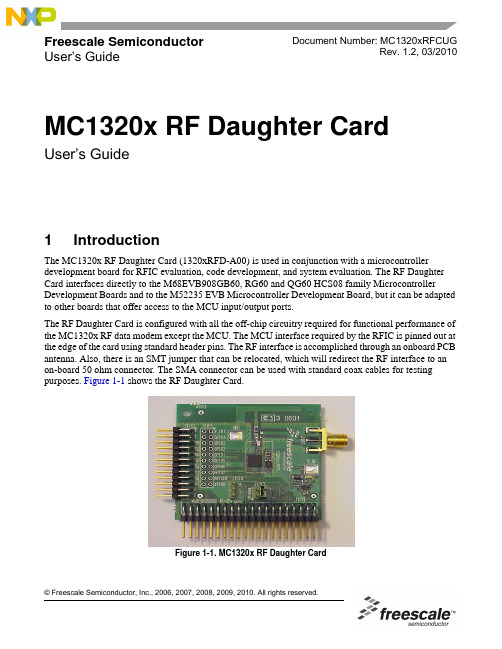
Freescale Semiconductor User’s GuideDocument Number: MC1320xRFCUGRev. 1.2, 03/20101IntroductionThe MC1320x RF Daughter Card (1320xRFD-A00) is used in conjunction with a microcontroller development board for RFIC evaluation, code development, and system evaluation. The RF Daughter Card interfaces directly to the M68EVB908GB60, RG60 and QG60 HCS08 family Microcontroller Development Boards and to the M52235 EVB Microcontroller Development Board, but it can be adapted to other boards that offer access to the MCU input/output ports.The RF Daughter Card is configured with all the off-chip circuitry required for functional performance of the MC1320x RF data modem except the MCU. The MCU interface required by the RFIC is pinned out at the edge of the card using standard header pins. The RF interface is accomplished through an onboard PCB antenna. Also, there is an SMT jumper that can be relocated, which will redirect the RF interface to an on-board 50 ohm connector. The SMA connector can be used with standard coax cables for testing purposes. Figure 1-1 shows the RF Daughter Card.Figure1-1. MC1320x RF Daughter CardMC1320x RF Daughter CardUser’s GuideIntroductionFigure1-2 shows the RF Daughter Card installed in a GB60 development board.Figure1-2. MC1320xRF Daughter Card In GB60 Development Board Figure1-3 shows the M52235 EVB development board.Figure1-3. M52235 EVB Development BoardSafety Information 2Safety InformationAny modifications to this product may violate the rules of the Federal Communications Commission and make operation of the product unlawful.47 C.F.R. Sec. 15.21This equipment has been tested and found to comply with the limits for a Class B digital device, pursuant to part 15 of the FCC Rules. These limits are designed to provide reasonable protection against harmful interference in a residential installation. This equipment generates uses and can radiate radio frequency energy and, if not installed and used in accordance with the instructions, may cause harmful interference to radio communications. However, there is no guarantee that interference will not occur in a particular installation. If this equipment does cause harmful interference to radio or television reception, which can be determined by turning the equipment off and on, the user is encouraged to try to correct the interference by one or more of the following measures:•Reorient or relocate the receiving antenna.•Increase the separation between the equipment and receiver.•Connect the equipment into an outlet on a circuit different from that to which the receiver is connected.•Consult the dealer or an experienced radio/TV technician for help.47 C.F.R. Sec.15.105(b)This equipment complies with FCC radiation exposure limits set forth for an uncontrolled environment. The antenna(s) used for this equipment must be installed to provide a separation distance of at least 8 inches (20cm) from all persons.This device complies with Part 15 of the FCC Rules. Operation is subject to the following two conditions:•This device may not cause harmful interference.•This device must accept any interference received, including interference that may cause undesired operation.3Revision HistoryThe following table summarizes revisions to this document since the previous release (Rev 1.1).Revision HistoryLocation RevisionSection 6Updated document cross reference.MC1320x MCU Interface4MC1320x MCU InterfaceFigure4-1 shows the typical connections between the MC1320x transceiver and a microcontroller unit (MCU). See the MC13202/203 Reference Manual, document MC13202RM, for interface considerations. Details about the interconnects for both the GB60 and M52235 Development boards are described in Section5.1, “Development Board Interconnects”. ArrayFigure4-1. MCU Interface PinoutDaughter Card Description 5Daughter Card DescriptionAs shown in Figure5-1 and Figure8-1, connector J101 is the main interface to the GB60 Development Board. The interface connections described in Section5.1, “Development Board Interconnects”, fall under the following three broad categories:1.Serial Peripheral Interface (SPI)2.Control3.PowerFigure1-2 shows how the RF Daughter Card is mounted on the GB60 Development Board.NOTEEnsure that zero ohm resistor R104 is in place on the MC1320x DaughterCard. As of this release, previous versions of the MC1320x Daughter Cardmay not have R104 inserted.NOTEJ101 Pin 1 of the MC1320x must to be connected to GB_PORT Pin 1 of theGB60 Development Board.As shown in Figure5-1 and Figure8-1, connector J102 is the main interface to the M52235 Development Board. Figure1-3 shows how the RF Daughter Card is mounted on the M52235 Development Board.NOTEJ102 Pin 1 of the MC1320x must be connected to MCU_PORT Pin 1 on theM52235 Development Board.Figure5-1 shows the top side of the RF Daughter Card PCB with component placement.Figure5-1. MC1320x Daughter Card (Top View)Daughter Card DescriptionFigure5-2 shows the shows the bottom side of the RF Daughter Card PCB.Figure5-2. MC1320x Daughter Card (Bottom View)5.1Development Board InterconnectsThe following sections describe the interconnects for both the GB60 and M52235 Development boards. Table5-1 lists the pin connections for J101 and Table5-2 lists the pin connections for J102.Table5-1. J101 Pin ConnectionsPin Number Pin Name Description Functionality1,2,3,4, 6,7,8,9, 10,11,12,15,16,17 18,21,23,25,26,28, 29, 30,33N/C No connection.5PTA2Connects to PTA2 on GB60.Provides a wakeup function to the MCU via Pin22 when jumper is installed between J103 pins1 and 2.13GPIO1Connects to General PurposeInput/Output 1 of MC1320X.When gpio_alt_en, Register 9, Bit 7 = 1, GPIO1 functions as an “Out of Idle” Indicator.14GPOI2Connects to General PurposeInput/Output 2 of MC1320X.When gpio_alt_en, Register 9, Bit 7 = 1, GPIO2 functions as a “CRC Valid” Indicator.Daughter Card Description19IRQConnects to IRQ pin of MC1320X.Allows the MC1320X to issue an IRQ to theMCU.20RESETOptionally connects to RESET of MC1320X when R101 or R102 are installed.Allows the MCU to reset the MC1320X.22PTE1/RXD1Connects to PTE1/RXD1 of GB60.Provides a wakeup function to the MCU via Pin5 when jumper is installed between J103 pins 1 and 2.24XCLK/16MHz Connects to CLKO of MC1320Xwhen jumper is installed between J103 pins 3 and 4.Provides reference based on MC1320X 16 MHz reference oscillator to the MCU.27PTC2/BAUD SEL Connect to PTC2/BAUD SEL ofGB60.31RXTXENConnect to RXTXEN of MC1320X.Allows the MCU to control the RXTXEN line ofthe MC1320X.32RESETConnects to RESET of MC1320X.Allows the MCU to reset the MC1320X.34PTD5/CESI/A TTN Connects to PTD5/CESI of GB60when R104 is installed. Connectdirectly to Pin 15 of J102.Allows the MCU to wake up the MC1320X from Doze or Hibernate.35MOSIConnect to MOSI of MC1320x.SPI36SPSCKConnect to SPICLK of the MC13201.SPI37CE Connect to CE of MC1320X.SPI38MISO Connects to MISO of MC1320X.SPI39V_INConnects the Daughter Card to the supply voltage output of the GB60 board.Provides supply voltage to the Daughter Card. Voltage must not exceed 16 Vdc. See Section 5.1.0.3, “Power Connections”.40GNDConnect ground on GB60 board to ground on Daughter Card.Table 5-1. J101 Pin Connections (continued)Pin NumberPin Name DescriptionFunctionalityDaughter Card DescriptionTable5-2. J102 Pin ConnectionsPin Number Pin Names Description Functionality 4, 5, 6, 7, 8, 11, 12, 14,16, 18, 22N/C No connection1V_IN Connects the Daughter Card to thesupply voltage output on theM52235EVB.Provides supply voltage to the Daughter Card. Voltage must not exceed 16 Vdc. See Section5.1.0.3, “Power Connections”.2IRQ Connects to IRQ pin of MC1320X.Allows the MC1320X to issue an IRQ to theMCU.3GND Connects the ground of the RFDaughter Card to the ground of theM52235EVB9GPIO1Connects to General PurposeInput/Output 1 of MC1320X.When gpio_alt_en, Register 9, Bit 7 = 1, GPIO1 functions as an “Out of Idle” Indicator.10GPOI2Connects to General PurposeInput/Output 2 of MC1320X.When gpio_alt_en, Register 9, Bit 7 =1, GPIO2 functions as a “CRC Valid” Indicator.13RESET Connects to RESET of MC1320Xand Pin 32 of J101.Allows the MCU to reset the MC1320X.15PTD5/CESI Connects to ATTN of MC1320Xand Pin 34 of J101.Allows the MCU to wake up the MC1320X from Doze or Hibernate.17MOSI Connects to MOSI of MC1320X.SPI19MISO Connects to MISO of MC1320X.SPI20RXTXEN Connect to RXTXEN of MC1320X.Allows the MCUntrol the RXTXEN line of theMC1320X.21SPICLK Connect to SPICLK of theMC1320XSPI23PTE2/CE-QSPI-CSO Connects to Pin 1 of J104Allows Chip Enable (CE) selection.See Section5.1.0.1, “SPI Connections”.24PTE2/CE-AN7Connects to Pin 3 of J104Allows Chip Enable (CE) selection.See Section5.1.0.1, “SPI Connections”.Daughter Card DescriptionNOTEIn the following sections, pin numbers not in parenthesis reference theGB60 Development Board. Pin numbers in parenthesis reference theM52235 Development Board.5.1.0.1SPI ConnectionsJ101 pins 35 through 38 (J102 pin 17, 19, 21 and 23) provide the following four wire SPI interface:•MOSI•SPICLK•CE•MISOThe MC1320x always functions as a slave device. SPI operation is described in detail in the appropriate MC1320x Data Sheet and/or MC1320x Reference Manual.NOTEAs it applies to the M52235 Development Board, the CE signal on (J102 Pin23 and Pin 24) are hard wired to header J104. These pins control thefunctionality of CE.When Pin 2 and Pin 3 of J104 are shorted, CE is wired to (J102 Pin 24)(PTE2/CE-AN7).When Pin 1 and Pin 2 of J104 are shorted, CE is wired to (J102 Pin 23)(PTE2/CE-QSPI_CS0).5.1.0.2Control Connections•J101 Pin 19 (J102 Pin 2) is the IRQ line from the MC1320x. Connection to the MCU depends on how the MCU services interrupts.•J101 Pin 31 (J102 Pin 20), RXTXEN, allows the MCU to initiate transceiver functions.•J101 Pin 34 (J102 Pin 15), ATTN, allows the MCU to wake up the MC1320x from Doze or Hibernate low power modes.NOTERXTXEN and ATTN are also available at header J105 for manual control.•J101 Pin 24 provides the MC1320x CLKO to the MCU when a jumper is installed at J103.•J101 Pin 32 (J102 Pin13) interfaces with the MCU to provide a Reset to the MC1320x.•J101 Pin 5 and Pin 22 provide a wake up function to the MCU when a jumper is installed at J103.•J101 Pin 13 and Pin 14 (J102 Pin 9 and Pin 11) provide access to the MC1320x GPIO1 and GPIO2 ports.RF Circuit5.1.0.3Power ConnectionsJ101 Pin 39 (J102 pin 1) provides the supply voltage to the RF Daughter Card. V oltage on this line should never exceed 16.0 VDC and the nominal voltage supply should not exceed 16.0 VDC. J101 Pin 40 (J102 pin 3) is ground.NOTEMCU connection signals are dependent on the on-board voltage regulator.If R105, D101, and C101 are mounted and R115 is removed, J101 Pin 39will provide the interface supply voltage which must never exceed 3.6 V.Nominal supply voltage should never exceed 3.4 V.5.1.0.4Non-MCU ConnectionsHeader J105 provides connections to a number of MC1320x contacts for non-MCU connections. As already stated, the RXTXEN and ATTN lines are available at J105 for external control using switches or other hardware. The MC1320x GPIO is also available for connection to external hardware.6RF CircuitThe MC1320x has an internal TX/RX switch. This feature allows for an external RF circuit that has a very low component count. The MC1320x requires only a few passive components and a balun to provide an interface to an antenna or a 50 ohm circuit. Figure6-1 shows a schematic for only the RF portion of the MC1320x Daughter Card.Figure6-1. RF Portion of 20x Daughter CardSoftware Configuration To provide a design that is of the lowest possible cost to produce, this reference design was built on a printed circuit board consisting of only two layers and with a printed circuit board antenna. The antenna is an Inverted F design widely used in the 2.4 GHz band. This antenna provides good performance while minimizing Bill of Material (BOM) cost.For more information on a low cost design approach, see the ZigBee Hardware Design Considerations Reference Manual (ZHDCRM)7Software ConfigurationAs shown in Figure8-1, the legend in the schematic shows the recommended jumper settings for Wake, ClkOut, and Chip Enable.NOTEThe Wake and ClkOut signals are only for interface to the GB60Development Board. The Chip Enable signal is only for interface to theM52235 Development Board.For software development, Freescale recommends users obtain the most recent software development tools and documentation from the following web pages:•For ZigBee related software and documentation go to /zigbee•For microcontroller software and documentation go to Bill of Materials (BOM) and Schematic8Bill of Materials (BOM) and Schematic This section contains the RF Daughter Card BOM and schematic.Table8-1. Bill of MaterialsQty Part Number ValueRatingToleranceManufacturer Part Number Reference196000310100Label 21*6mmTest BarCode96000310100BARCODE101350610710001100nF16V±10% X7R Murata GRM155R71C104KA88D C103, C104,C105050610710001100nF16V±10% X7R Murata GRM155R71C104KA88D C101 (NotMounted)2506208100011µF 6.3V±10% X5RMurata GRM188R60J105KA01D C102, C1060506208100011µF 6.3V±10% X5R Murata GRM188R60J105KA01D C108 (NotMounted)05061061000010nF16V±10% X7R Murata GRM155R71E103KZ01E C107(NotMounted)153300833001 3.3µF10V20%Vishay Sprague293D335X0010A2TE3C109250210268000 6.8pF50V±0.25pF NP0/C0GMurata GRM1555C1H6R8DZ01J C110, C11115021031000010pF50V±5% NP0/C0GMurata GRM1555C1H100JZ01D C112150210210000 1.0pF50V±0.25pF NP0/C0GMurata GRM1555C1H1R0CZ01D C113040110003303MM3Z3V3T1G 3.3V/200mW5%ONSemiconductorMM3Z3V3T1G D101 (NotMounted)141100017001Green_LED Citizen CL-170G-CD-T D102135501320200MC13202FreescaleSemiconductorMC13202IC101 134000298109LP2981IM5-3.3-40 to +125°C National LP2981IM5-3.3 NOPB IC1021200304040012*20p PinHeader - RightAnglemot/molex70216-4010-89-4402J1011200304024012*12p PinHeader - RightAnglemot/molex70216-2410-89-4242J1021200304004002*2p PinHeaderAMP0-826632-2J103 120030400300jumper_1x3AMP826629-3J104Bill of Materials (BOM) and Schematic200304020082*10 Pin HeaderAMP1-826632-0J105 (Not Mounted)120150700202SMA_edge_Re ceptacle_Fema lemot/sma-end_launch 142-0701-831J106220030000100ProbeLoop TobyElectronics TP-107-02-5-T J107, J108254710518001 1.8nH 300mA ±0.3nH TOKO LL1005-FHL1N8S L101, L102254710539002 3.9nH ±0.3nHTOKO LL1005-FHL3N9S L103, L104171000566010fsl566-1FreescaleSemiconductor FSL566-1 FR4 0.76mm PCB1014611000000010R 62.5mW/25V 5%YAGEO RC0402JRE070RL R103, R112, R115,R1040611000000010R62.5mW/25V 5%YAGEORC0402JRE070RLR101, R102 (NotMounted)061100410001100R 62.5mW/25V 5%YAGEO RC0402JRE07100RL R105 (Not Mounted)06110061000110K62.5mW/25V 5%YAGEORC0402JRE0710KLR106, R107, R108, R110 (NotMounted)161100747000470K 62.5mW/25V 5%YAGEO RC0402JRE07470KL R109161100422000220R 62.5mW/25V 5%YAGEO RC0402JRE07220RL R1111611200000010R 125mW/150V 5%YAGEO RC0805JRE070RL R1130611200000010R 125mW/150V 5%YAGEO RC0805JRE070RL R114 (Not Mounted)15813091600416.000MHz ±20ppm ±20ppmKDS ZD00882X101156360240001LDB212G4005C-001MurataLDB212G4005C-001Z101Table 8-1. Bill of MaterialsQty Part Number Value Rating ToleranceManufacturer Part Number ReferenceNOTESHow to Reach Us:Home Page:E-mail:*********************USA/Europe or Locations Not Listed:Freescale SemiconductorTechnical Information Center, CH3701300 N. Alma School RoadChandler, Arizona 85224+1-800-521-6274 or +1-480-768-2130*********************Europe, Middle East, and Africa:Freescale Halbleiter Deutschland GmbHTechnical Information CenterSchatzbogen 781829 Muenchen, Germany+44 1296 380 456 (English)+46 8 52200080 (English)+49 89 92103 559 (German)+33 1 69 35 48 48 (French)*********************Japan:Freescale Semiconductor Japan Ltd.HeadquartersARCO Tower 15F1-8-1, Shimo-Meguro, Meguro-ku,Tokyo 153-0064, Japan0120 191014 or +81 3 5437 9125***************************Asia/Pacific:Freescale Semiconductor Hong Kong Ltd.Technical Information Center2 Dai King StreetTai Po Industrial EstateTai Po, N.T., Hong Kong+800 2666 8080**************************For Literature Requests Only:Freescale Semiconductor Literature Distribution Center P.O. Box 5405Denver, Colorado 802171-800-521-6274 or 303-675-2140Fax: 303-675-2150*********************************************Information in this document is provided solely to enable system and software implementers to use Freescale Semiconductor products. There are no express or implied copyright licenses granted hereunder to design or fabricate any integrated circuits or integrated circuits based on the information in this document.Freescale Semiconductor reserves the right to make changes without further notice to any products herein. Freescale Semiconductor makes no warranty, representation or guarantee regarding the suitability of its products for any particular purpose, nor does Freescale Semiconductor assume any liability arising out of the application or use of any product or circuit, and specifically disclaims any and all liability, including without limitation consequential or incidental damages. “Typical” parameters that may be provided in Freescale Semiconductor data sheets and/or specifications can and do vary in different applications and actual performance may vary over time. All operating parameters, including “Typicals”, must be validated for each customer application by customer’s technical experts. Freescale Semiconductor does not convey any license under its patent rights nor the rights of others. Freescale Semiconductor products are not designed, intended, or authorized for use as components in systems intended for surgical implant into the body, or other applications intended to support or sustain life, or for any other application in which the failure of the Freescale Semiconductor product could create a situation where personal injury or death may occur. Should Buyer purchase or use Freescale Semiconductor products for any such unintended or unauthorized application, Buyer shall indemnify and hold Freescale Semiconductor and its officers, employees, subsidiaries, affiliates, and distributors harmless against all claims, costs, damages, and expenses, and reasonable attorney fees arising out of, directly or indirectly, any claim of personal injury or death associated with such unintended or unauthorized use, even if such claim alleges that Freescale Semiconductor was negligent regarding the design or manufacture of the part.Freescale™ and the Freescale logo are trademarks of Freescale Semiconductor, Inc. All other product or service names are the property of their respective owners.© Freescale Semiconductor, Inc. 2006, 2007, 2008, 2009, 2010. All rights reserved.。
Freescale msCAN教程

Nicrosystem NSCF51AC-R1开发板教程-------CAN 总线教程作者Bluehacker <QQ: 282074921> /bluehacker 版本V 1.0 日期2010年8月25日 版权说明 本教程以Nicrosystem 开发的NSCF51AC-R1型低成本飞思卡尔coldfire V1开发板为平台,但相关内容应该适用于其他公司开发的飞思卡尔coldfire V1或S08开发板,甚至对其他非飞思卡尔MCU 也有借鉴作用。
我们通过网络免费提供此教程电子版本,不收取任何费用,您可以自由下载传播,但请您不要更改本教程中的任何文字、图片、表格;更不得以任何形式声称拥有本教程的版权,侵占作者的劳动成果。
本教程可能有描述不当或错误之处,欢迎你指正,但作者和作者所在公司单位不对可能的错误负任何责任。
备注如果你发现本教程的问题,欢迎您通过 nicrosystem@ 与我们联系。
也欢迎你关注我们的产品和在电子论坛上的活动作者的博客:/bluehackerNicrosystem “我们的freescale ”专栏:/forum-100-1.htmlNicrosystem 定期在与非网社区开展系列针对飞思卡尔处理器的diy 活动和助学活动:Nicrosystem EDN “我们的freescale”小组:/2460/淘宝:一. CAN总线的特点和历史●什么是CAN?CAN,全称为“Controller Area Network”,即控制器局域网,是国际上应用最广泛的现场总线之一。
最初,CAN被设计作为汽车环境中的微控制器通讯,在车载各电子控制装置ECU 之间交换信息,形成汽车电子控制网络。
比如:发动机管理系统、变速箱控制器、仪表装备、电子主干系统中,均嵌入CAN控制装置。
一个由CAN 总线构成的单一网络中,理论上可以挂接无数个节点。
实际应用中,节点数目受网络硬件的电气特性所限制。
飞思卡尔芯片简介

• RS08微控制器—S08內核的簡化版, 在某些應用領域更有效,更便宜。 例如簡單的電子機械設備遷移到固態 控制。 • S08微控制器—從通用HC08微控制器 轉化而來。總線速度更快,操作電壓 更低,S08更適用于電池供電的應用。 • ColdFire嵌入式控制器—可兼容,
微處理器
歡迎來到飛思卡爾獨家 推出的微控制器集
/contiuum
/continuum
飛思卡爾公司 的優勢
飛思卡爾公司是嵌入式控制領域的全球 帶頭人,是MCU技術的先驅,並是主要 技術創新者。我們開發了首個基于flash 存儲的MCU。微控制器集提供了接觸我 們市場主導產品的簡單方法。全套的工 具、培訓和支持,包括常規開發工具、 參考設計、應用筆記和網上直播。使得 你的設計更快捷。
關于微控制器集
飛思卡爾公司的微控制器集是業界首個也是唯一一個8位到32位兼容產品的路線圖。從入門 級的RS08和S08控制器到全特征的ColdFire產品,微控制器集使用相同的外圍模塊和開發工 具,簡化了設計過程並縮短推向市場的時間。逐步兼容即可將微控制器集內的設備從低端 到高端遷移到下一個兼容的設備上。例如:將MC9S08JM60 (JM60)遷移到MCF51JM128 (JM128)上,然後只要花少量時間和精力就可遷移到MCF5221x MCUs。 在優化產品性能,價格和功能時,您可能會產生從8位轉到32位的需求,反之亦然。您只要簡 單地更換板上的控制器,重新編譯代碼。微控制器集的8位和32位的連接點是我們的FlexisTM 系列微控制器。
8 KB SRAM
MCF51JM128:
• 50.33MHz V1 ColdFire 內核 • 25.17MHz總線頻率 • 2.7-5.5V的操作電壓 • 80引腳LQFP,64引腳LQFP, 64引腳QFP,44 引腳LQFP封裝
飞思卡尔半导体用户指南说明书

Freescale Semiconductor User’s Guide1OverviewThe Freescale Freedom development platform is a set of software and hardware tools for evaluation and development. It’s ideal for the rapid prototyping ofmicrocontroller-based applications. The Freescale Freedom KL26Z hardware (FRDM-KL26Z) is a capable and cost-effective design featuring a Kinetis L seriesmicrocontroller, the industry’s first microcontroller built on the ARM® Cortex™-M0+ core.FRDM-KL26Z can be used to evaluate the KL16 and KL26 Kinetis L series devices. It features a KL26Z128VLH4, a device boasting a maximum operating frequency of 48MHz, 128KB of flash, a full-speed USB controller, and numerous analog and digital peripherals. The FRDM-KL26Z hardware is form-factor compatible with the Arduino™ R3 pin layout, providing a broad range of expansion board options. The on-board interfaces include an RGB LED, a 6-axis digital sensor (combining a 3D accelerometer and 3Dmagnetometer), ambient light sensor, and a capacitive touch slider.The FRDM-KL26Z features the Freescale open standard embedded serial and debug adapter known as OpenSDA.Doc Number:FRDMKL26ZUGRev. 0, 10/2013Contents1.Overview . . . . . . . . . . . . . . . . . . . . . . . . . . . . . . . . . . . 12.Reference documents . . . . . . . . . . . . . . . . . . . . . . . . . 23.Getting started . . . . . . . . . . . . . . . . . . . . . . . . . . . . . . . 24.FRDM-KL26Z hardware overview . . . . . . . . . . . . . . 25.FRDM-KL26Z hardware description . . . . . . . . . . . . . 5FRDM-KL26Z User’s GuidebyFreescale Semiconductor, Inc.Reference documentsThis circuit offers several options for serial communications, flash programming and run-control debugging.2Reference documentsThe table below provides a list of reference documents for the FRDM-KL26Z hardware. All of these documents are available online at /FRDM-KL26Z.Table1. FRDM-KL26Z reference documentsFilename DescriptionFRDM-KL26Z Quick Start Package Quick Start Guide and supporting files for getting started with the FRDM-KL26Z FRDM-KL26Z User’s Guide This document—overview and detailed information for the FRDM-KL26ZhardwareFRDM-KL26Z Pinouts Spreadsheet of pin connections for all MCU pins. Includes pinout for the I/Oheaders, Arduino R3 compatibility chart, and OpenSDA MCU pinout.FRDM-KL26Z Schematics PDF schematics for the FRDM-KL26Z hardwareFRDM-KL26Z Design Package Zip file containing all design source files for the FRDM-KL26Z hardware OpenSDA User’s Guide Overview and instructions for use of the OpenSDA embedded debug circuit3Getting startedSee the FRDM-KL26Z Quick Start Package for step-by-step instructions to get started with the FRDM-KL26Z. See the Jump Start Your Design section on /FRDM-KL26Z for the Quick Start Package and software lab guides.4FRDM-KL26Z hardware overviewThe features of the FRDM-KL26Z include:•MKL26Z128VLH4 in a 64 LQFP package•Capacitive touch slider•FXOS8700CQ accelerometer and magnetometer•Tri-color (RGB) LED•Ambient light sensor•User push button•Flexible power supply options – USB, coin cell battery, external source•Battery-ready, power-measurement access points•Easy access to MCU I/O via Arduino™ R3 compatible I/O connectors•Programmable OpenSDA debug interface with multiple applications available including:—Mass storage device flash programming interface—P&E Debug interface provides run-control debugging and compatibility with IDE toolsFRDM-KL26Z hardware overview—CMSIS-DAP interface: new ARM standard for embedded debug interface—Data logging applicationFigure1 shows a block diagram of the FRDM-KL26Z design. The primary components and their placement on the hardware assembly are pointed out in Figure2.Figure1. FRDM-KL26Z block diagramFRDM-KL26Z hardware overview! (Figure2. FRDM-KL26Z feature call-outsFRDM-KL26Z hardware description5FRDM ‐KL26Z hardware description5.1Power supplyThere are multiple power supply options on the FRDM-KL26Z. It can be powered from either of the USB connectors, the VIN pin on the I/O header, an on-board coin cell battery, or an off-board 1.71-3.6V supply from the 3.3V pin on the I/O header. The USB and VIN supplies are regulated on-board using a 3.3V linear regulator to produce the main power supply. The other two sources are not regulated on-board. Table 2 provides the operational details and requirements for the power supplies.Table 2.Power supply requirementsNote that the OpenSDA circuit is only operational when a USB cable is connected and supplying power to J10. However, protection circuitry is in place to allow multiple sources to be powered at once.Figure 3 shows the schematic drawing for the power supply inputs and the on-board voltage regulator.Figure 3. Power supply schematicIn addition, regulated power can be supplied to J3 pin 10 from an external source through P5-9V_VIN by populating the board with an optional voltage regulator, e.g. a 7805 style regulator in a TO-220 package, thus providing a high current supply to external devices. To prevent voltage sag under a high load, C23,Supply Source Valid RangeOpenSDA Operational?Regulated on-board?OpenSDA USB (J7)5V Yes Yes KL26Z USB (J5)5V No Yes V in 4.3-9V No Yes 3.3V pin 1.71-3.6V No No Coin cell battery1.71-3.6VNoNoFRDM-KL26Z hardware descriptionC24, C25 & C28 should be populated with appropriately sized capacitors to match the regulator chosen. See Figure4.Figure4. Optional voltage regulator schematicTable3. FRDM-KL26Z power suppliesPowerDescriptionSupply NameP5-9V_VIN Power supplied from the V in pin of the I/O headers (J3 pin 16)P5V_SDA Power supplied from the OpenSDA USB connector (J10). A Schottky diode provides back drive protection.P5V_KL26Z Power supplied from the KL26Z USB connector (J6). A Schottky diode provides back drive protection P3V3_VREG Regulated 3.3V supply. Sources power to the P3V3 supply rail with an optional back drive protection Schottky diode.12P3V3_BATT Coin cell battery supply voltage. Sources power to the P3V3 supply rail with the option of adding a back drive protection Schottky diode.3P3V3Main supply rail for the FRDM-KL26Z assembly. May be sourced from P3V3_VREG, P3V3_BATT, or directly from the I/O headers (J3 pin 8).P3V3_KL26Z KL26Z MCU supply. Header J5 provides a convenient means for energy consumption measurements.4 P3V3_SDA OpenSDA circuit supply. Header J15 provides a convenient means for energy consumptionmeasurements.4P5V_USB Nominal 5V supplied to the I/O headers (J3 pin 10). Sourced from either the P5V_KL26Z or P5V_SDA supply through a back drive protection Schottky diode.FRDM-KL26Z hardware description5.2Serial and debug adapter (OpenSDA)OpenSDA is an open standard serial and debug adapter. It bridges serial and debug communications between a USB host and an embedded target processor as shown in Figure 5. The hardware circuit is based on a Freescale Kinetis K20 family microcontroller (MCU) with 128 KB of embedded flash and anintegrated USB controller. OpenSDA features a mass storage device (MSD) bootloader, which provides a quick and easy mechanism for loading different OpenSDA applications such as flash programmers, run-control debug interfaces, serial-to-USB converters, and more. See the OpenSDA User’s Guide for more details.Figure 5. OpenSDA high-level block diagramOpenSDA is managed by a Kinetis K20 MCU built on the ARM® Cortex™-M4 core. The OpenSDA circuit includes a status LED (D8) and a pushbutton (SW2). The pushbutton asserts a reset signal to the KL26Z target MCU. It can also be used to place the OpenSDA circuit into Bootloader mode. OpenSDA MCU RESET can be isolated from SW2 by cutting the trace between pins on J13. SPI and GPIO signals1By default the linear regulator, U1, is a 3.3V output regulator. However, this is a common footprint that would allow the user to modify the assembly to utilize an alternative device such as a 1.8V or 2.5V regulator. The KL26Z microcontroller has an operating range of 1.71V to 3.6V.2D2 is bypassed by J14. By default, the pins of J14 are shorted together, to reduce the voltage drop across D2. To use D2, cut the trace between the pins of J14.3If a coin cell battery is to be used, add a small amount of solder to the coin cell ground pad before adding the battery holder. Also, it is recommended to populate D1 as a protection diode when using a coin cell battery.4J5 and J15 are not populated by default. The two pins of these headers are in parallel with 0 Ω resistors. In addition, J5 is also in parallel with a 10 Ω resistor. To measure the energy consumption of the KL26Z, either a voltmeter or an ammeter may be used. To use a voltmeter, R3 (0 Ω) must be removed before connecting the voltmeter probes to the pins of J5. Both R3 and R2 (10 Ω) must be removed to measure current with an ammeter. For the OpenSDA MCU, energy consumption can be measured by removing R4 (0 Ω) and connecting ammeter probes to the pins of J15.FRDM-KL26Z hardware descriptionprovide an interface to the SWD debug port of the KL26Z. Additionally, signal connections are available to implement a UART serial channel. The OpenSDA circuit receives power when the USB connector J10 is plugged into a USB host.5.2.1Debug interfaceSignals with SPI and GPIO capability are used to connect directly to the SWD of the KL26Z. These signals are also brought out to a standard 10-pin (0.05”) Cortex Debug connector (J7). It is possible to isolate the KL26Z MCU from the OpenSDA circuit and use J7 to connect to an off-board MCU. To accomplish this, cut the trace on the bottom side of the PCB that connects J8 pin 1 to J8 pin 2. This will disconnect the SWD_CLK pin to the KL26Z so that it will not interfere with the communications to an off-board MCU connected to J7.Figure6. SWD debug connectorNote that J7 is not populated by default. A Samtec FTSH-105-02-F-D or compatible connector can be added to the J7 through-hole connector. A mating cable, such as a Samtec FFSD IDC cable, can then be used to connect from the OpenSDA of the FRDM-KL26Z to an off-board SWD connector.5.2.2Virtual serial portA serial port connection is available between the OpenSDA MCU and pins PTA1 and PTA2 of the KL26Z. Several of the default OpenSDA Applications provided by Freescale, including the MSD Flash Programmer and the P&E Debug Application, provide a USB communications device class (CDC) interface that bridges serial communications between the USB host and this serial interface on the KL26Z.5.3KL26Z microcontrollerThe target microcontroller of the FRDM-KL26Z is the KL26Z128VLH4, a Kinetis L series device in a 64 LQFP package. The KL26Z MCU features include:FRDM-KL26Z hardware description•32-bit ARM Cortex-M0+ core—Up to 48 MHz operation—Single-cycle fast I/O access port•Memories—128 KB flash—16 KB SRAM•System integration—Power management and mode controllers—Low-leakage wakeup unit—Bit manipulation engine for read-modify-write peripheral operations—Direct memory access (DMA) controller—Computer operating properly (COP) Watchdog timer•Clocks—Clock generation module with FLL and PLL for system and CPU clock generation—4 MHz and 32 kHz internal reference clock—System oscillator supporting external crystal or resonator—Low-power 1kHz RC oscillator for RTC and COP watchdog•Analog peripherals—16-bit SAR ADC w/ DMA support—12-bit DAC w/ DMA support—High speed comparator•Communication peripherals—Two 16-bit Serial Peripheral Interfaces (SPI)—USB dual-role controller with built-in FS/LS transceiver—USB voltage regulator—Two I2C modules—One low-power UART and two standard UART modules—One I2S module•Timers—One 6-channel Timer/PWM module—T wo 2-channel Timer/PWM modules—2-channel Periodic Interrupt Timer (PIT)—Real time clock (RTC)—Low-power Timer (LPTMR)—System tick timer•Human-Machine Interfaces (HMI)—General purpose input/output controllerFRDM-KL26Z hardware description—Capacitive touch sense input interface hardware module5.3.1Clock sourceThe Kinetis KL26 microcontrollers feature an on-chip oscillator compatible with three ranges of input crystal or resonator frequencies: 32-40 kHz (low freq. mode), 3-8 MHz (high frequency mode, low range) and 8-32 MHz (high frequency mode, high range). The KL26Z128 on the FRDM-KL26Z is clocked from an 8 MHz crystal.5.3.2USB interfaceThe Kinetis KL26 microcontrollers feature a dual-role USB controller with on-chip full-speed andlow-speed transceivers. The USB interface on the FRDM-KL26Z is configured as a full-speed USB device. J6 is the USB connector for this interface.Figure7. USB connector schematicIn order to enable USB host functionality on the FRDM-KL26Z, it is necessary to populate J9 and R8 as shown in Figure7. However, there is no electrical protection provided. Use the USB host functionality at your own risk.FRDM-KL26Z hardware description 5.3.3Serial portThe primary serial port interface signals are PTA1 and PTA2. These signals are connected to both the OpenSDA and to the J1 I/O connector. Note that the OpenSDA connection can be isolated from J1 by removing R13 & R14, if required.5.3.4ResetThe PTA20/RESET signal on the KL26Z128 is connected externally to a pushbutton, SW2, and also to the OpenSDA circuit. However, J13 has been provided to isolate the OpenSDA MCU from SW2. Isolating the RESET line allows a more accurate measurement of the target device’s power consumption in low-power modes. The reset button can be used to force an external reset event in the target MCU. The reset button can also be used to force the OpenSDA circuit into bootloader mode. See Section5.2, “Serial and debug adapter (OpenSDA), for more details.5.3.5DebugThe sole debug interface on all Kinetis L Series devices is a serial wire debug (SWD) port. The primary controller of this interface on the FRDM-KL26Z is the onboard OpenSDA circuit (see Section5.2, “Serial and debug adapter (OpenSDA)). However, an unpopulated 10-pin (0.05”) Cortex Debug connector, J7, provides access to the SWD signals. The Samtec FTSH-105-02-F-D or compatible connector can be added to the J7 through-hole debug connector to allow for an external debug cable to be connected.5.4Capacitive touch sliderTwo Touch Sense Input (TSI) signals, TSI0_CH9 and TSI0_CH10, are connected to capacitive electrodes configured as a touch slider. Freescale’s Touch Sense Software (TSS) provides a software library for implementing the capacitive touch slider.5.56-axis accelerometer and magnetometerA Freescale FXOS8700CQ low-power, six-axis accelerometer and magnetometer is interfaced through an I2C bus and two GPIO signals as shown in Table4. By default, the I2C address is 0x1D (SA0 pulled high).Table4. Accelerometer signal connectionsFX0S8700CQ KL26Z128SCL PTE24SDA PTE25INT1PTD0INT2PTD1FRDM-KL26Z hardware descriptionFigure 8. FXOS8700CQ schematic diagram5.6RGB LEDThree PWM-capable signals are connected to a red, green, blue LED, D7. The signal connections are shown in Table 5.Table 5. RGB LED signal connectionsFigure 9. RGB LED schematic diagramRGB LEDKL26Z128Red cathodePTE29Green cathodePTE31Blue cathodePTD511PTD5 is also connected to the I/O header on J2 pin 10 (also known as D13).FRDM-KL26Z hardware description5.7Ambient light sensorAn ambient light sensor is connected to ADC0_SE3 (PTE22). This sensor may be isolated from PTE22 by removing R36.5.8Input/Output connectorsThe KL26Z128VLK4 microcontroller is packaged in a 64-pin LQFP. Some pins are utilized in on-board circuitry, but many are directly connected to one of four I/O headers.The pins on the KL26Z microcontroller are named for their general purpose input/output port pin function. For example, the 1st pin on Port A is referred to as PTA1. The I/O connector pin names are given the same name as the KL26Z pin connected to it, where applicable.FRDM-KL26Z hardware descriptionNote that all pinout data is available in spreadsheet format in FRDM-KL26Z Pinouts. See Section2, “Reference documents” for details.5.9Analog reference voltageThe onboard ADC of the KL26Z128VLH4 MCU uses the Reference V oltage High (VREFH) and Reference V oltage Low (VREFL) pins to set high and low voltage references for the analog modules. On the FRDM-KL26Z, by default VREFH is attached to P3V3_KL26Z (3.3V Supply). VREFL is connected to GND. Figure10 illustrates this circuitry.Figure10. FRDM-KL26Z VREFH circuit schematicIf desired, VREFH can use a VDDA independent reference by adding R11 and a Zener diode (D6). R10 (0 Ω resistor) must be removed when implementing this option. Alternatively, VREFH can be attached to an external source through AREF by removing R10 and populating R9 with a 0 Ω resistor.5.10Arduino compatibilityThe I/O headers on the FRDM-KL26Z are arranged to allow compatibility with peripheral boards (known as shields) that connect to Arduino™ and Arduino-compatible microcontroller boards. The outer rows of pins (the even numbered pins) on the headers share the same mechanical spacing and placement as the I/O headers on the Arduino Revision 3 (R3) standard.FRDM-KL26Z hardware descriptionRefer to the FRDM-KL26Z Pinouts spreadsheet for a compatibility chart showing how all the functions of the KL26Z signals on the I/O connectors map to the pin functions available on the Arduino Uno R3.Document Number:FRDMKL26ZUG Rev. 010/2013Information in this document is provided solely to enable system and software implementers to use Freescale products. There are no express or implied copyright licenses granted hereunder to design or fabricate any integrated circuits based on the information in this document.Freescale reserves the right to make changes without further notice to any products herein. Freescale makes no warranty, representation, or guarantee regarding the suitability of its products for any particular purpose, nor does Freescale assume any liability arising out of the application or use of any product or circuit, and specifically disclaims any and all liability, including without limitation consequential or incidental damages. “Typical” parameters that may be provided in Freescale data sheets and/or specifications can and do vary in different applications, and actual performance may vary over time. All operating parameters, including “typicals,” must be validated for each customer application by customer’s technical experts. Freescale does not convey any license under its patent rights nor the rights of others. Freescale sells products pursuant to standard terms and conditions of sale, which can be found at the following address: /SalesTermsandConditions.How to Reach Us:Home Page:Web Support:/supportFreescale, the Freescale logo, and Kinetis are trademarks of FreescaleSemiconductor, Inc., Reg. U.S. Pat. & Tm. Off. ARM is the registered trademark ofARM Limited. ARM Cortex-M0+ is the trademark of ARM Limited. All other product orservice names are the property of their respective owners.© 2013 Freescale Semiconductor, Inc.。
飞思卡尔的品牌延伸

飞思卡尔多媒体处理器i.MX品牌延伸之路摘要:本文通过对品牌延伸战略的理论回顾,结合飞思卡尔半导体公司的多媒体处理器芯片i.MX品牌通过不断细分市场来采取的产品线延伸战略,评价其品牌延伸战略的优缺点,同时指出进行品牌延伸需要考虑的管理原则。
最后总结飞思卡尔i.MX品牌的品牌延伸并为公司今后的品牌战略提出了建议。
关键词:飞思卡尔,i.MX,品牌延伸,细分市场1. 飞思卡尔以及其i.MX品牌介绍飞思卡尔半导体公司介绍[1]飞思卡尔(Freescale Semiconductor)是美国的半导体生产厂商,于2004年由原摩托罗拉的半导体部门组建(摩托罗拉于2003年10月宣布剥离飞思卡尔,飞思卡尔在2004年7月上市)。
飞思卡尔是全球领先的半导体公司,为汽车、消费、工业、网络和无线市场设计并制造嵌入式半导体产品。
企业总部位于美国德克萨斯州奥斯汀,在全球30多个国家和地区拥有设计、研发、制造和销售机构。
如今的飞思卡尔半导体已经成为全球最大的半导体公司之一,在全球30多个国家拥有员工24,000人,2007年的总销售额达到57亿美元,拥有专利5,900项,投入研发投资每年12亿美元。
拥有客户达10,000多个,其中包括全球前100位原始设备制造商。
飞思卡尔在全球共有七个晶圆制造厂和两个组装测试厂。
在中国多个城市设有分支机构,销售分支遍布热点城市。
在苏州、上海、天津和北京有设计中心。
并在天津有较大规模的工厂,主要从事封装和测试等。
主要为汽车、网络、无线通信、工业控制和消费电子等行业提供产品。
通过嵌入式处理器和辅助产品,为客户提供复杂多样的半导体和软件集成方案,即飞思卡尔所谓的“平台级产品”。
飞思卡尔全球现有1万个终端客户,其中包括由公司自己的销售队伍服务的100多家知名的原始设备生产商,以及通过数千个代理商网络服务的其他终端客户。
自从2004年成立以来,飞思卡尔半导体一直处于变革与调整中。
2005年登陆资本市场;2006年被收归于私募基金旗下;2007年淡出全球十大半导体公司名单;2008年退出手机芯片业务、重组MRAM业务;2011年5月重新回归资本市场、12月再次进行产品部门调整。
- 1、下载文档前请自行甄别文档内容的完整性,平台不提供额外的编辑、内容补充、找答案等附加服务。
- 2、"仅部分预览"的文档,不可在线预览部分如存在完整性等问题,可反馈申请退款(可完整预览的文档不适用该条件!)。
- 3、如文档侵犯您的权益,请联系客服反馈,我们会尽快为您处理(人工客服工作时间:9:00-18:30)。
万联芯城供应原装正品freescale飞思卡尔集成电路,价格较同行更有优势,提交BOM配单,立即为您报价,采购原装电子元器件,就上万联芯城,为客户解决物料需求,节省采购成本!
点击进入万联芯城
飞思卡尔半导体公司是一家总部位于德克萨斯州奥斯汀的美国跨国公司,在19个国家的75个地点设计,研发,制造和销售业务。
飞
思卡尔在全球雇佣了17,000名员工。
2015年12月7日,恩智浦半导体以大约118亿美元的现金和股票完成了与飞思卡尔[2]的合并。
飞思卡尔代理_freescale代理股东每股飞思卡尔代理_freescale代理普通股获得62.5亿美元现金和
0.351英镑的恩智浦股票。
包括飞思卡尔代理_freescale代理债务的假设,购买价格约为167亿美元。
飞思卡尔代理_freescale代理是全球首批半导体公司之一,于1948年开始在亚利桑那州凤凰城担任摩托罗拉分公司[3],随后于2004年剥离摩托罗拉半导体产品部门。
1955年,用于汽车收音机的摩托罗拉晶体管是世界上第一款商用大功率晶体管。
它也是摩托罗拉首款批量生产的半导体器件。
在20世纪60年代,美国太空计划的目标之一是将一个人登陆月球并将他安全地送回地球。
1968年,美国宇航局开始载人阿波罗飞行,导致1969年7月首次登月。
阿波罗计划对数百名参与设计,测试和生产电子设备的员工尤为重要。
摩托罗拉终成为飞思卡尔代理
_freescale代理半导体的分部,提供数千个半导体设备,地面跟踪和检测设备,以及12个车载跟踪和通信单元。
Apollo命令模块中的“向上数据链路”接收来自地球的信号以转发到其他机载系统。
转
发器接收并传输语音和电视信号以及科学数据。
[4]
同年,[需要澄清]摩托罗拉的技术被用于推出首款带有全晶体管电源和汽车接收器的双向移动无线电。
[5]
摩托罗拉在未来几年继续在网络和通信领域取得增长,提供无线电转发器背后的工具,并在1973年继续开发第一个模拟移动电话的原型。
[6]
飞思卡尔代理_freescale代理的第一个微处理器(MC6800 8位)于1974年推出,用于汽车,计算和视频游戏应用。
[7]
摩托罗拉的下一代32位微处理器MC68000引领了1984年推动计算革命的技术浪潮,为Apple,Commodore,Atari,Sega,Sun和Hewlett-Packard等公司的设备供电。
[8]
在20世纪90年代,摩托罗拉的技术成为防抱死制动系统智能电源开关的驱动力,这是汽车安全气囊的首批微机电系统(MEMS)惯性传感器之一,而摩托罗拉的MPC5200微处理器则为通用汽车的OnStar系统部署了远程信息处理系统。
从那时起,飞思卡尔代理_freescale代理继续为微处理器提供消费,医疗,网络和汽车产品的技术,为世界上第一台无管道无线胰岛素泵[10]和用于高效发动机设计的汽车微控制器提供技术支持。
飞思卡尔代理_freescale代理的动作感应加速度计为Guitar Hero视频游戏的互动提供了动力。
[11]全球首屈一指的电子阅读器处理器供应商是飞思卡尔代理_freescale代理。
[12] 2009年,飞思卡尔代理
_freescale代理展示了世界上低的启动电压单电感器DC / DC转换器,用于太阳能和热电能量收集应用。
[13]
2011年,飞思卡尔代理_freescale代理推出业界首款可从小型到大型电池扩展的多模无线基站处理器系列 - 集成DSP和通信处理器技术,实现真正的“基站级芯片”。
[14]此外,近ABI Research市场研究报告指出,飞思卡尔代理_freescale代理拥有射频(RF)半导体器件市场60%的份额。
同样在2011年,飞思卡尔代理_freescale代理宣布推出飞思卡尔代理_freescale代理第一款用于智能移动设备位置跟踪的磁力计。
[15]凭借迈凯轮电子系统公司的合作,他们帮助NASCAR Sprint Cup系列车辆从2012年开始从化油器转换为燃油喷射。
[16] [17] [18]
2014年3月8日,飞思卡尔代理_freescale代理宣布其20名员工乘
坐马来西亚航空公司370航班。
搭载飞思卡尔代理_freescale代理员工的这架飞机失踪了[19],其中一小部分是在一年后发现的。
2015年3月,宣布了一项合并协议,飞思卡尔代理_freescale代理半导体将通过该协议被恩智浦半导体收购,并将合并这些公司,形成40美元(相当于2017年的41.30美元)亿美元公司。
[20] [21]此次收购于2015年12月7日结束。
2013年2月26日,飞思卡尔代理_freescale代理半导体宣布推出世界上体积小的ARM供电芯片。
Kinetis KL02的尺寸为1.9 x 2毫米,是一个完整的微控制器单元(MCU),意味着该芯片支持处理器,RAM,ROM,时钟和I / O控制单元。
该芯片与Atmel M0 +产品竞争,后者是业内低功耗的领导者。
[22] 飞思卡尔代理_freescale代理称这些芯片可以用于可吞服的计算机。
飞思卡尔代理_freescale代理已经与各种健康和保健客户合作。
Fitbit和OmniPod胰岛素泵都使用飞思卡尔代理_freescale代理芯片。
新芯片于2013年2月26日至28日在德国纽伦堡的“嵌入式世界”展出。
[23]
到目前为止,已知具有包含ARM Cortex-M0 +内核的前导字母代码L,E,M,W和包含ARM Cortex-M4内核的字母代码K或KW的设备(另请参见飞思卡尔代理_freescale代理产品列表中的相关部分)。
QorIQ是恩智浦半导体(前身为飞思卡尔代理_freescale代理)的ARM架构和基于Power Architecture的通信微处理器品牌。
QorIQ 品牌以及P1,P2和P4产品系列于2008年6月宣布.P3和P5产品的详细信息于2010年公布.QorIQ Layerscape产品系列于2013年宣布,基于Cortex A7,Cortex A9,A15,A53和 A72核心在ISA不可知的Layerscape架构上。
2014年8月,飞思卡尔代理_freescale代理半导体为消费和汽车应用推出了一系列完全可编程的无线充电芯片和参考设计。
新芯片组经认证可与无线电源联盟的Qi无线标准和Power Matters Alliances 充电规范配合使用。
[24]
飞思卡尔代理_freescale代理主要专注于汽车应用,在瑞萨电子的汽车应用市场份额排名第二。
由于这种关注和曝光,预计像Zipcar 这样的汽车共享应用将对未来的飞思卡尔代理_freescale代理收入产生重大负面影响。
摩托罗拉宣布他们的半导体部门将于2003年10月6日被剥离,以创建飞思卡尔代理_freescale代理。
飞思卡尔代理_freescale代理于2004年7月16日完成首次公开募股。
2006年9月15日,飞思卡尔代理_freescale代理同意以Blackstone Group及其共同投资者Carlyle Group,TPG Capital和Permira为首的财团以176亿美元收购。
[26] 在公司股东投票后,收购要约于2006年11月13日被接受。
此次收购于2006年12月1日结束,是对戴尔2013年收购之前技术公司的大私人收购,并且是有史以来大的十大收购之一。
[27]
飞思卡尔代理_freescale代理于2011年2月11日申请上市,并于2011年5月26日完成首次公开募股。
飞思卡尔代理_freescale代理在纽约证券交易所上市,股票代码为FSL。
在首次公开募股时,飞思卡尔代理_freescale代理的账面上有76亿美元的未偿债务,[28]飞思卡尔代理_freescale代理正在接受与此次首次公开募股有关的不当行为的调查。
[29]。