电源芯片-TD6810英文-Datasheet
芯片英文对照表
芯片英文对照表Inrush current (cold start) 突增电流 (冷开机)Efficiency: 60% Min. At nominal line 效率: 60%,一般电压(指115/230V,除非另有说明)Noise test 噪声测试Static output characteristics 静态输出特性Dynamic output characteristics 动态输出特性Rise time DC输出电压上升时间Hold up time DC输出电压持续时间Protection: 保护OVP (over voltage protection) 过电压保护OPP (over power protection ) 过功率保护OCP (over current protection) 过电流保护OTP (over temp. protection) 过温度保护Short circuit protection 短路保护Hi-pot (dielectric withstand voltage) 耐电压测试4.1 Primary to secondary AC TO DC 初级对次级4.2 Primary to safety ground AC TO FG 初级对地4.3 Secondary to safety ground DC TO FG 次级对地4.4 Insulation resistance 绝缘阻抗4.5 Leakage current 漏电流SPEC (规格) 常用单词Model: 机种 revision: 版本 issued date: 发行日期P/n: 品名 description: 说明 remark: 备注Reported by: 草拟 checked by: 审核 approved by: 核准2. FN (factory notice):生产通知/ECN (engineering change notice)工程变更通知2.1 FN: Immediated change 立即变更 Running change 自然切换2.2 ECN: old rev. new rev. drawing no. customer alteration ref.旧版本新版本图号客户变更依据3.Department 部门3.1 MFG: manufacturing3.1.1 AI: auto insertion 自动插件3.1.2 preforming 预加工3.1.3 SMD 表面黏着3.2 QA: quality assurance3.2.1 VQA 进料品质保证3.2.2 PQC,FQC 制程品管3.2.3 Calibration , safety 仪校,安规3.3 PE: production engineering 制造工程3.3.1 TE: test engineering 测试工程3.3.2 ME: mechanical engineering 机械工程3.3.3 IE: industrial engineering 工业工程3.4 HR: human resources 人力资源3.5 Material 材料3.5.1 PC: production control 生管 3.5.2 purchasing 采购3.5.3 warehouse仓库3.6 ENG: engineering 工程3.6.1 document control 资料中心4.Safety4.1 UL (Underwriters Laboratories) 美国保险协会实验室4.2 CSA (Canadian Standards Association) 加拿大标准协会4.3 TUV 德国技术监护协会4.4 VDE 德国电气标准4.5 NEMKO 挪威电气标准4.6 DEMKO 丹麦电气标准5.Other 其它FAX( 传真 ): date, to, fm, subject, dear, TKS, best regards,FAR: issue, description, corrective action, preventive action, analysis, defect,Failure, supplier / vendorISO: International Organization for Standardization 国际标准化组织Quality Manual: 品质手册Procedure: 作业程序6. Vocabulary:6.1 contraction 缩写 Contraction 缩写6.2 component 零件 AQL: accept quality lever 允收水准6.3 process 制程 ATS: auto test system 自动测试系统6.4 electrical 电气 CR: critical 严重6.5 time 时间 ESD: electrostatic discharge 静电放电6.7 non 动词 ICT: in-circuit test 场效晶体管6.8 color 颜色 MA: major 主要MI: minor 次要MRB: material review board 不良材料审核组NTC: negative temperature characteris热敏电阻O/I: operation instruction 工作指导书PWM: pulse width modification 波宽调整S/N: series number 序号SMD: surface mounting device 表面黏着WIP: work in progress 半成品(工作进行中)JIT: just in timeIR: infra-red 红外线的PDPC: process, decision, Program, chartQCCA: quality control Circle activities 品管圈活动CWQC: company-wide Quality controlMCR 代用词Component (零件)Bobbin 线轴 tape 胶带Bridge 桥式整流 tapping screw 自攻螺丝Cable tie 束带 terminal 端子Capacitor 电容 transformer(XFMR) 变压器Case 外壳 transistor 电晶体Ceramic capacitor 陶瓷电容 tube 套管Chip capacitor 芯片电容 varistor 突波吸收器Chip resistor 芯片电阻 VR (variable resistance) 可变电阻Choke 线圈 washer 垫片Connector 连接器 zener 齐纳Control board 基板Diode(dio) 二极管 process (制程)Epoxy 脂 assembly 组立Fan 风扇 burn-in (B/I) 崩应FET 埸效晶体管 component 零件Filter滤波器 flux 助焊剂Fuse clip 保险丝座 function test 功能测试Fuse holder 保险丝座 gravity 比重Glue 胶 Hi-pot test 耐高压测试Heatsink 散热片 insertion 插件Fuse 保险丝 ORT 可靠度测试IC 集成电路 packing 包装Inductor 电感 solder machine 锡炉Insulator 绝缘片 station 站别Jumper wire 跳线 supplier/vender 厂商Label 标签 temperature 温度Lock washer 接地星形垫片 torque 扭距NTC 热敏电阻 touch-up(T/U) 补焊Nut 螺丝帽 date code 周期Output cable 输出线 Time (时间)Output wire 输出线 Jan. 一月PCB 电路板 Feb. 二月Photo couple 光藕合二极管 Mar. 三月Regulator 稳压器 Apr. 四月Resistor 电阻 May. 五月Rivet 柳钉 Jun. 六月Screw 螺丝 Jul. 七月Socket 插座 Aug. 八月Solder bar 锡棒 Sept. 九月Spring washer 弹簧垫片 Oct. 十月Stand-off 支柱 Nov. 十一月Star washer 星形垫片 Dec. 十二月Switch 开关CRT (cathode-ray tube) 示波器Anode 阳(正,板)极DCGP 常用单词COMPONERT (零件) 2. PROCESS (制程) Resistor(res) 电阻 pre-forming 加工成型VR(variable) 可变电阻 component 零件Chip resistor` 芯片电阻 process 制程Capacitor(cap) 电容 insertion 插件Ceramic capacitor 陶磁电容 solder machine 锡炉Choke 线圈 gravity 比重Inductor 电感 temperature 温度Transformer(X’FNR) 变压器 touch-up(T/U) 补焊Bobbin 线轴 burn-in(B/I) 崩应Fuse 保险丝 assembly 组立Fuse holder 保险丝座 torque 扭力Fuse clip 保险丝座 packing 包装RTC 热敏电阻 flux 助焊剂Varistor 突波吸收器Diode(dio) 二极管Photo couple 光藕合二极管Zener 齐纳 3. ELECTRICAL (电气)Bridge diode 桥式整流Transistor 电晶体 input(I/P) 输入IC 集成电路 output(O/P) 输出Filter 滤波器 regulation 调整FET 埸效电晶体 specification 规格Regulation 稳压器 ripple 涟波PCB 电路板 noise 噪声Control board 小基板 noise buzz 无音Fan 风扇 protection 保护Case 外壳 OVP 过电压保护Switch 开关 OCP 过电流保护Socket 插座 OPP 过功率保护Screw 螺丝 no output(NOP) 无输出Tapping screw 自动螺丝 broken/blow out (BRO) 烧机Nut 螺帽 short 短路Washer 垫片 open 开路Spring washer 弹簧垫片 voltage 电压Star washer 星形垫片 current 电流Lock washer 接地星形垫片 frequency 频率Output wire 输出线 load 负载Output cable 输出线 full load 满载Cable tie 束带 low load 轻载Connector 连接器 damage 损坏Rivet 铆钉 oscilloscope 示波器Terminal 端子 test 测试Stand-off 支柱 adjust 调整Heatsink 散热片 inspection 检验Insulator 绝片 hi-pot test 高压测试Tape 胶带 grounding 接地Tube 套管Label caution 标签(警告标签) Epoxy 脂Glue 胶Jumper wire 跳线。
LT-6710_6750_6810说明书

II.2.B 测试环境设定 ...................................................................................................... 17 II.2.B.A II.2.B.B II.2.B.C II.2.B.D II.2.B.E II.2.B.F II.2.B.G II.2.B.H 测试文件类型................................................................................................ 18 测试结果显示................................................................................................ 18 测试结果统计................................................................................................ 18 测试结果打印................................................................................................ 18 控制信号输出模式 ......................................................................................... 19 不良品锁定 ................................................................................................... 19 测试警报声 ................................................................................................... 19 不良品连续警报声 ......................................................................................... 19
焊机常用电源芯片
焊机常用电源芯片(中英文实用版)英文文档:Title: Common Power Supply Chips for Welding MachinesWelding machines are essential tools in various industries, and their performance is highly dependent on the quality and type of power supply chips used.Power supply chips play a crucial role in regulating and stabilizing the power output of welding machines, ensuring consistent and reliable welding operations.One commonly used power supply chip in welding machines is the integrated circuit (IC) controller.This chip is responsible for managing the flow of electricity and maintaining the desired output voltage and current levels.It protects the machine from overcurrent, overvoltage, and short-circuit conditions, ensuring safe and reliable operation.Another essential type of power supply chip used in welding machines is the voltage regulator.This chip ensures that the voltage supplied to the welding torch and other components remains stable, regardless of fluctuations in the input voltage.Voltage regulators are available in different types, such as linear regulators and switching regulators, each offering specific advantages in terms of efficiency and size.Furthermore, power supply chips for welding machines often includeprotection features, such as overtemperature protection and undervoltage lockout.These features help prevent damage to the welding machine due to excessive heat or low voltage conditions, extending the lifespan of the equipment.In conclusion, the choice of power supply chips for welding machines is crucial for achieving optimal performance, reliability, and safety.By selecting the appropriate power supply chips, welders can ensure efficient and consistent welding operations, even in challenging environments.中文文档:标题:焊接机常用电源芯片焊接机是各种行业中不可或缺的工具,其性能在很大程度上取决于所使用电源芯片的质量和类型。
100V NPN 达林顿接驱电源芯片 SOT23 产品说明书
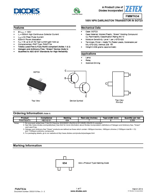
100V NPN DARLINGTON TRANSISTOR IN SOT23Features∙ BV CEO > 100V ∙ I C = 900mA high Continuous Collector Current ∙ I CM = 5A Peak Pulse Current ∙ 625mW Power dissipation ∙ h FE > 5k up to 2A for high current gain hold up ∙ Complementary PNP Type: FMMT734 ∙ Totally Lead-Free & Fully RoHS compliant (Notes 1 & 2) ∙ Halogen and Antimony Free. “Green” Device (Note 3) ∙ Qualified to AEC-Q101 Standards for High ReliabilityMechanical Data∙ Case: SOT23 ∙ Case Material: Molded Plastic, “Green” Molding CompoundUL Flammability Classification Rating 94V-0 ∙ Moisture Sensitivity: Level 1 per J-STD-020 ∙ Terminals: Finish – Matte Tin Plated Leads, Solderable perMIL-STD-202, Method 208 ∙ Weight 0.008 grams (approximate)Applications∙ Lamp ∙ Relay ∙ Solenoid DrivingOrdering Information (Note 4)Product Compliance Marking Reel size (inches) Tape width (mm)Quantity per reelFMMT634TA AEC-Q101 634 783,000Notes: 1. No purposely added lead. Fully EU Directive 2002/95/EC (RoHS) & 2011/65/EU (RoHS 2) compliant. 2. See /quality/lead_free.html for more information about Diodes Incorporated’s definitions of Halogen and Antimony free, "Green" and Lead-Free. 3. Halogen and Antimony free "Green” products are defined as those which contain <900ppm bromine, <900ppm chlorine (<1500ppm total Br + Cl) and <1000ppm antimony compounds.4. For packaging details, go to our website at /products/packages.htmlMarking Information634 = Product Type Marking CodeSOT23Top View Pin-OutTop ViewDevice SymbolCEB624634 EAbsolute Maximum Ratings(@T A = +25°C, unless otherwise specified.)UnitValueCharacteristic SymbolCollector-Base Voltage V CBO120 VCollector-Emitter Voltage V CEO100 VEmitter-Base Voltage V EBO12 VContinuous Collector Current I C900 mAPeak Pulse Current I CM 5 AThermal Characteristics (@T A = +25°C, unless otherwise specified.)UnitValueCharacteristic SymbolPower Dissipation (Note 5) P D625 mWPower Dissipation (Note 6) P D806 mWThermal Resistance, Junction to Ambient (Note 5) RθJA200 ︒C/WThermal Resistance, Junction to Ambient (Note 6) RθJA155 ︒C/WThermal Resistance, Junction to Leads (Note 7) RθJL194 ︒C/WOperating and Storage Temperature Range T J, T STG-55 to +150 ︒CESD Ratings (Note 8)UnitClassJEDECValueCharacteristic SymbolElectrostatic Discharge - Human Body Model ESD HBM 2,000 V 2Electrostatic Discharge - Machine Model ESD MM 200 V BNotes: 5. For a device mounted with the exposed collector pad on 25mm x 25mm 1oz copper that is on a single-sided 1.6mm FR4 PCB; device is measuredunder still air conditions whilst operating in a steady-state.6. Same as note (5), except the device is measured at t ≤ 5 sec.7. Thermal resistance from junction to solder-point (at the end of the collector lead).8. Refer to JEDEC specification JESD22-A114 and JESD22-A115.Thermal Characteristics and Derating information100m1101001m 10m100m110Single Pulse T amb =25°CV CE(s at)Limited100µs1ms10ms100ms1s DCSafe Operating AreaI C C o l l e c t o r C u r r e n t (A )V CE Collector-Emitter Voltage (V)2550751001251501750.00.10.20.30.40.50.60.7Derating CurveTemperature (°C)M a x P o w e r D i s s i p a t i o n (W )20406080100120140160180200220Transient Thermal ImpedanceT h e r m a l R e s i s t a n c e (°C /W )Pulse Width (s)0.1110100Pulse Power DissipationPulse Width (s)M a x i m u m P o w e r (W )Electrical Characteristics (@T A = +25°C, unless otherwise specified.)Characteristic Symbol Min Typ Max Unit Test ConditionCollector-Base Breakdown Voltage BV CBO 120 170 - V I C = 100µACollector-Emitter Breakdown Voltage (Note 9) BV CEO 100 115 - V I C = 10mAEmitter-Base Breakdown Voltage BV EBO 12 16 - V I E = 100µA Collector Cut-off Current I CBO - <1 10 nA V CB = 80V Emitter Cut-off Current I EBO - <1 10 nA V EB = 7V Collector Emitter Cut-off Current I CES - <1 100 nA V CES = 80VStatic Forward Current Transfer Ratio (Note 9) h FE- 20k 15k 5k - - 50k 60k 40k 14k 24k 600 ---- - - - I C = 10mA, V CE = 5V I C = 100mA, V CE = 5V I C = 1A, V CE = 5V I C = 2A, V CE = 5V I C = 1A, V CE = 2V I C = 5A, V CE = 5VCollector-Emitter Saturation Voltage (Note 9) V CE(sat)- - - - - - 0.67 0.72 0.75 0.82 0.68 0.85 0.750.800.850.93 - 0.96 V I C = 100mA, I B = 1mA I C = 250mA, I B = 1mA I C = 500mA, I B = 5mA I C = 900mA, I B = 5mA I C = 900mA, I B = 5mA, T J =+150°C I C = 1A, I B = 5mABase-Emitter Saturation Voltage (Note 9) V BE(sat) - 1.5 1.65 V I C = 1A, I B = 5mA Base-Emitter Turn-On Voltage (Note 9) V BE(on) - 1.33 1.50 V I C = 1A, V CE = 5VTransition Frequency f T- 140 - MHz I C = 50mA, V CE = 10V,f = 100MHzOutput Capacitance C obo - 9 20 pF V CB = 10V, f = 1MHz Turn-On Time t (on) - 290 - ns V CC = 20V, I C = 500mA,I B1 = -I B2 = 1mATurn-Off Time t (off) - 2,400 - ns Notes:9. Measured under pulsed conditions. Pulse width ≤ 300µs. Duty cycle ≤ 2%Typical Electrical Characteristics (@T A = +25°C, unless otherwise specified.)Package Outline DimensionsPlease see AP02002 at /datasheets/ap02002.pdf for latest version.Suggested Pad LayoutPlease see AP02001 at /datasheets/ap02001.pdf for the latest version.Note:For high voltage applications, the appropriate industry sector guidelines should be considered with regards to creepage and clearance distancesbetween device Terminals and PCB tracking.SOT23Dim Min Max Typ A 0.37 0.51 0.40 B 1.20 1.40 1.30 C 2.30 2.50 2.40 D 0.89 1.03 0.915 F 0.45 0.60 0.535 G 1.78 2.05 1.83 H 2.80 3.00 2.90 J 0.013 0.10 0.05 K 0.890 1.00 0.975 K1 0.903 1.10 1.025 L 0.45 0.61 0.55 L1 0.25 0.55 0.40 M 0.085 0.150 0.110 a 8°All Dimensions in mmDimensions Value (in mm)Z 2.9 X 0.8 Y 0.9C2.0 E1.35 X EYCZA l l 7°IMPORTANT NOTICEDIODES INCORPORATED MAKES NO WARRANTY OF ANY KIND, EXPRESS OR IMPLIED, WITH REGARDS TO THIS DOCUMENT, INCLUDING, BUT NOT LIMITED TO, THE IMPLIED WARRANTIES OF MERCHANTABILITY AND FITNESS FOR A PARTICULAR PURPOSE (AND THEIR EQUIVALENTS UNDER THE LAWS OF ANY JURISDICTION).Diodes Incorporated and its subsidiaries reserve the right to make modifications, enhancements, improvements, corrections or other changes without further notice to this document and any product described herein. Diodes Incorporated does not assume any liability arising out of the application or use of this document or any product described herein; neither does Diodes Incorporated convey any license under its patent or trademark rights, nor the rights of others. Any Customer or user of this document or products described herein in such applications shall assume all risks of such use and will agree to hold Diodes Incorporated and all the companies whose products are represented on Diodes Incorporated website, harmless against all damages.Diodes Incorporated does not warrant or accept any liability whatsoever in respect of any products purchased through unauthorized sales channel. Should Customers purchase or use Diodes Incorporated products for any unintended or unauthorized application, Customers shall indemnify and hold Diodes Incorporated and its representatives harmless against all claims, damages, expenses, and attorney fees arising out of, directly or indirectly, any claim of personal injury or death associated with such unintended or unauthorized application.Products described herein may be covered by one or more United States, international or foreign patents pending. Product names and markings noted herein may also be covered by one or more United States, international or foreign trademarks.This document is written in English but may be translated into multiple languages for reference. Only the English version of this document is the final and determinative format released by Diodes Incorporated.LIFE SUPPORTDiodes Incorporated products are specifically not authorized for use as critical components in life support devices or systems without the express written approval of the Chief Executive Officer of Diodes Incorporated. As used herein:A. Life support devices or systems are devices or systems which:1. are intended to implant into the body, or2. support or sustain life and whose failure to perform when properly used in accordance with instructions for use provided in thelabeling can be reasonably expected to result in significant injury to the user.B. A critical component is any component in a life support device or system whose failure to perform can be reasonably expected to cause thefailure of the life support device or to affect its safety or effectiveness.Customers represent that they have all necessary expertise in the safety and regulatory ramifications of their life support devices or systems, and acknowledge and agree that they are solely responsible for all legal, regulatory and safety-related requirements concerning their products and any use of Diodes Incorporated products in such safety-critical, life support devices or systems, notwithstanding any devices- or systems-related information or support that may be provided by Diodes Incorporated. Further, Customers must fully indemnify Diodes Incorporated and its representatives against any damages arising out of the use of Diodes Incorporated products in such safety-critical, life support devices or systems.Copyright © 2014, Diodes Incorporated。
6810h参数

6810h参数
6810H是一款由PWM电流驱动的双极低功耗电机驱动集成芯片,由工采网代
理。
以下是该芯片的主要参数和特性:
1.驱动方式:采用Pala-IN的驱动方式,工作电压范围为10V~32V。
2.输出能力:具有两路H桥驱动,最大输出为32V/1.0A。
3.封装和散热:采用eTSSOP20 173mil封装,可以有效改善散热性能,符合Rohs规范,
且为无铅产品,引脚框架采用100%无锡电镀。
4.电流衰减模式:电流衰减模式可选择为快衰减、慢衰减和混合衰减,且可以任意设
置快衰减与慢衰减的比例,从而更平稳高效的控制电机驱动。
5.电源需求:采用单一电源供电,可以有效地简化系统级设置的难度。
6.功率输出模块:由N型功率MOSFET组成H桥电路,包含整流电路和限流电路。
7.控制接口:提供简单的并行数字控制接口。
8.睡眠模式:提供一种低功耗睡眠模式来关断内部电路,以达到非常低的静态电流。
这种睡眠模式通过设置nSLEEP引脚来实现。
请注意,具体的应用和设计需求可能会影响参数的选择和使用。
因此,在选择和使用6810H芯片时,建议详细查阅相关的技术文档和参考资料,以确保正确理解和应用其参数和特性。
PN8360Datasheet英文版Rev.A.1503

PN8360Datasheet英文版Rev.A.1503 PN8360ChipownHigh Precision CC/CV Primary-Side ConverterGeneral DescriptionThe PN8360 consists of a high precision CC/CV primary side controller and a 650V power MOSFET, specifically designed for a high performance low power AC/DC charger and LED lighting with minimal external components. PN8360 operates in primary-side sensing and regulation, so opto-coupler and TL431 could be eliminated.PN8360 offers complete protection coveragewith automatic self-recovery feature including Cycle-by-Cycle current limiting protection (OCP), over voltage protection (OVP)and feedback loop open protection (OLP), over temperature protection (OTP) and short circuit protection etc. Internal HV Start-up circuit and the chip’s very low consumption help to meet the strict standby power standard. In CC control, the current and output power setting can be adjusted externally by the sense resistor Rcs at CS pin. In CV control, PFM operations are utilized to achievehigh performance and high efficiency. In addition, good load regulation is achieved by the built-in cable drop compensation.Features■Internal 650 V avalanche-rugged power MOSFET■±5% Constant current R egulation at Universal AC input■ Primary-side Sensing and Regulation Without TL431 and Opt coupler■ Programmable CV and CC Regulation■ Programmable Cable Drop Compensation■Built-in Primary winding inductance compensation ■ Internal HV Start-up Circuit■ Excellent Protection Coverage:Over Temperature Protection (OTP)VDD Under Voltage Lockout (UVLO)Cycle-by-Cycle Current Limiting (OCP)Open Loop Protection (OLP)VDD Over Voltage Protection (OVP)Auto- recovery protection ModeApplications■Switch AC/DC Adaptor and Battery Charger■ LED LightPackage/Order InformationVDDSWSWCSFBOrder codes Package VcableTypical power85~265 V ACPN8360SSC-R1 SOP73% 12WPN8360SSC-R1B SOP76% 12WPN8360SSC-R1C SOP70% 12WPN8360NEC-T1 DIP8 3% 15WPN8360NEC-T1B DIP86% 15WPN8360NEC-T1C DIP80% 15W Typical ApplicationPin DefinitionsTable 1. Pin DefinitionsSOP-7 Pin NumberDIP-8 Pin NumberPin Name Pin Function Description11VDDPositive Supply voltage Input2 2 COMP Loop compensation3 3 FBThe voltage feedback from auxiliary winding. Connected to resistor divider from auxiliary winding reflecting output voltage 44CS Current Sense Input5 5 SWHV MOSFET Drain pin. The Drain pin is connected to the primary lead of the transformer.6 67 7,8 GND GroundTypical powerTable 2. Typical powerPart number Package85-265V ACPN8360SOP-7 12W DIP-8 15WNote:1. Maximum practical continuous power in adapter design at 45°C ambient temperature, with enough cooling conditions.Absolute Maximum RatingsSupply voltage Pin VDD…………………………………………………………………….….…..-0.3~25V High-V oltage Pin, SW…………………………………………………………………………….…650V Pin FB, CS, COMP……………………………………………………………………………...…-0.3~5.5V Operating Junction Temperature………………………………………………………………..…..-40~150℃ Package Thermal Tempera ture(SOP-7)……………………………………………...………… ……80°C/W Package Thermal Temperature(DIP-8)…………………………………………...…………………40°C/W Storage Temperature Range…………………………………………………………………………-55~150℃ Lead Temperature (Soldering, 10Secs)………………………………………………………………260℃ ESD voltage Protection (HBM)………………………………………………………………………4.0kV Pulse draincurrent……………………………………………………………………………………3. 0AElectrical CharacteristicsTable 3. Power section (T J =25°C, V DD = 17 V; unless otherwise specified)SYMBOLPARAMETERCONDITIONSMINTYPMAXUNIT V BVDSS Break-down voltage I SW = 250uA, T J = 25℃ 650 690 V I OFF Off-state drain current V SW = 500V 100uA R DS(on)Drain-source on state resistanceI SW = 1A,T J = 25℃2.5Table 4. Supply section (T J = 25°C, V DD = 17 V; unless otherwise specified)SYMBOLPARAMETERCONDITIONSMINTYPMAXUNITSUPPLY VOLTAGE SECTIONV SW_START Drain-source start voltage20 V I DD_CH Start up charging current V DD <v ddoff="" ,="" isw="" charge="" v="" dd="" -0.6="" -1="" -1.4="" ma<="" p="" bdsfid="185">。
桑德森标准产品数据表(数据表16810-A)2020年1月版说明书

Technical DataTechnical DaTa 25-16810-A January 2020 SpecificationSupply Voltage 15 to 30 VdcCable size / Type 0.5mm 2 ~ 2.5mm 2 /FIRETUF, FP200 or MICC Mounting Hole Centres 50 ~ 80mm Allowable Alarm Current25mA Allowable Remote Indicator Current25mAWiring hintsEach terminal is suitable for clamping up to 2 wires. Clamping of 2 wires of very different diameters under one screw is not recommended.DO NOT USE A POWER TERMINAL DRIVER.Suitable for mounting to mounting boxes with 50-80mm fixing centres.EFXN533 DoP044818EN54-7 Point Type Smoke Detectors EFXN525DoP044618EN54-5 Point Type Heat Detectors EFXN524DoP044518EN54-5 Point Type Heat Detectors EFXN526DoP044718EN54-5 Point Type Heat Detectors EFXN632DoP044918EN54-5 Point Type Heat Detectors EN54-7 Point Type Smoke DetectorsFXN922DoP0405122831Detector InstalledDetector RemovedE n d o f L i n e M o n i t o rE n d o f L i n e R e s i s t o rGeneralIf difficulty is experienced when mounting the detector, this may be due to the following:Wiring causing an obstruction - move or shorten wires. Although the base is tolerant to uneven mounting surfaces, a very uneven surface may cause the base to deform when the mounting screws are tightened down - loosen screws to reduce this or slide base to a more flat position.WaRninG: DO NOT USE HIGH VOLTAGE TESTERS WHEN DETECTORS OR CONTROL PANEL ARE CONNECTED TO THE SYSTEM.Zener Diode Switch action eFDB800 (cDB300 & MDB800)eatonEMEA Headquarters Route de la Longeraie 71110 Morges, Switzerland Eaton.euTEL: +44 (0) 1302 321541FAX: +44 (0) 1302 303220******************************************************© 2020 EatonAll Rights ReservedEaton is a registered trademark.All trademarks are property of their respective Eaton Electrical Systems Ltd.Wheatley Hall Road Doncaster DN2 4NBTEL: +44 (0) 1302 303303 FAX: +44 (0) 1302 367155Utilising locking T a bThe Mounting base includes an optional feature to prevent the removal of the detector without the use of a tool.1. Remove the standard fit retaining clip.2. Insert the locking clip which is located at the centre of the base as shown.Mount the detector onto the base as described in Detector Installation (see over) and rotate fully clockwise until it finally clicks.The detector is now locked into position. Remove by utilising a suitable tool (eg a thin screwdriver) into the hole in the detector cover. Gently push the tool into the detector and rotate anti-clockwise.BaseOrder Codes Conventional Photoelectric Smoke Detector - Cooper EFXN520(CDBB300 / FXN520)EFDB800(CDB300 / MDB800) EFXN533 Conventional Heat Detector - Class A2R - Cooper EFXN525Conventional Heat Detector - Class BS - Cooper EFXN524Conventional Heat Detector - Class CS - CooperEFXN526Conventional Photo/Thermal - Class A2S (Heat Performance) - Cooper EFXN632Bi-Wire Programmable Conventional Photoelectric, Photo/Thermal (A2S), Heat Detector (A1R, BS or CS) - JSBEFXN520(CDBB300 / FXN520)FXN922Detector Features (Photoelectric & Photo/Thermal)All Photoelectric and Photo/Thermal detectors, automatically compensate for gradual increases in the scatter signal due to contamination e.g. dust build up.Self-check Features Of The Bi-wire DetectorThe Self-Check feature monitors for the failure of the internal primary alarm circuitry.Under this condition, the detector will still register an alarm condition via the yellow LED. Following such a failure, the yellow LED will remain on following a reset, signaling a fault at the main panel and the detector must be replaced.BiWire detectors, automatically compensate for gradual increases in the scatter signal due to contamination e.g. dust build up. If excessive dust occurs, the yellow LED will show continuously. If this occurs, the maintenance procedure should be conducted.The yellow LED will also light continuously if the detectors optical sensor signal begins to reduce below its normal level (chamber monitoring).In addition, the BiWire range has an isolator that opens if the internal power fails in the detector, giving rise to a zone fault at the main panel.When used with a BiWire compatible panel with Self Check features, the BiWireDetectors range of detectors can be instructed to blink their yellow LED every 2 seconds by a command from the main panel, to aid the search for a break in the zone cabling or an open detector isolator.Detector installationFit detector to mounting base and rotate clockwise until the detector drops into place. Continue to rotate clockwise until the detector clicks into place and no further rotation is possible. If the detectors are required to be locked into position, refer to the ‘UtilisingLocking Tab’ section.Smoke detectors are supplied fitted with dust covers for general protection against airborne contaminates.These must be removed from all detectors before the fire system is commissioned.NB. These dust covers do not provide adequate protection against quantities of dust generated by building workT estingAll detectors must be tested following installation or routine service andmaintenance. It is recommended that these tests are carried out by a competent person. Authorised personnel must be informed that the fire system will betemporarily out of service before commencing testing. To prevent unwanted alarms, ensure that the the panel is in test mode and it may be appropriate to disable some or all of the sounder circuits.. When all tests are complete, restore panel to normal operation and notify authorised personnel that the system is operational.Smoke Detectors:Subject the detector to be tested to a controlled amount of an approved synthetic smoke aerosol via a smoke detector test pole. Suitable products are available for example, from No Climb Products Ltd.Check that the red LED on the detector latches into alarm within 30 seconds. If an optional remote LED is fitted, check that this also lights.Ensure that the control panel activates into alarm.Reset the detector from the control panel unless automatically reset by the panel in test mode.This procedure will test the smoke sensing circuitry of the Photo/Thermal Detector.heat Detectors:Using a heat gun or hair dryer capable of generating temperatures of up to 95°C,direct the heat source towards the heat sensing elements, visible through the side of the outer cover, from a distance of 15 to 30cm. Care should be taken not to allow the plastic surface temperature to exceed 110°C otherwise damage may occur.When the temperature reaches the ‘Alarm Temperature’ (see Specifications above), check that the red LED on the detector latches into alarm. If an optional remote LED is fitted, check that this also lights.Ensure that the control panel activates into alarm.Reset the detector from the control panel unless automatically reset by the panel in test mode.This procedure will test the heat sensing circuitry of the Photo/Thermal Detector.MaintenanceOnly minimal maintenance can be performed on this range of detectors as they do not contain any site serviceable parts. The frequency of maintenance and will depend on the environment towhich the detector is exposed but should be at least annually. Dusty or damp environments will demand more frequent maintenance.Remove the detector from its mounting base.Use a vacuum cleaner to remove dust build up from around the smoke entryapertures of a smoke detector, or from around the heat sensing element of a heat detector.For smoke detectors, visually inspect the insect mesh for blockages. If these can not be cleared by vacuuming, the detector must be replaced.Re-fit detector to its mounting base and test as described above.Detectors that fail the testing procedure must be replaced.EFXN533EFXN525EFXN524EFXN526EFXN632FXN922Operating voltage 15 to 30 Vdc 15 to 30 Vdc 15 to 30 Vdc 15 to 30 Vdc 15 to 30 Vdc 15 to 30 Vdc Standby current (max) 30μA 30μA 30μA 30μA 30μA 80μA Start up current (max 20 sec)340μA N/A N/A N/A 340μA 340μA Alarm current (max)25mA 25mA 25mA 25mA 25mA 25mAAmbient temperature (max)60ºC45ºC60ºC75ºC45ºCOpto Mode 60ºCOpto-Heat Mode 45°CA1R Rate of Rise Mode 45°C BS Fixed Temp Mode 60°C CS Fixed Temp Mode 80°C Ambient temperature (min)-20ºC -20ºC -20ºC -20ºC -20ºC -10ºCAlarm temperature (static)N/A60ºC77ºC90ºC60ºCOpto-Heat Mode 60°CA1R Rate of Rise Mode 60°C BS Fixed Temp Mode 77°C CS Fixed Temp Mode 92°C Heat detector class –as defined by EN54-5:2000N/A A2R BS CS A2S See above Relative humidity (non-condensing)0 to 95%0 to 95%0 to 95%0 to 95%0 to 95%0 to 95%Height (without base)34mm 43mm 43mm 43mm 43mm 43mm Height (with base)47mm 56mm 56mm 56mm 56mm 56mm Diameter 100.5mm 100.5mm 100.5mm 100.5mm 100.5mm 100.5mm Weight 78g 76g 76g 76g 78g 78g Material PC/ABS PC/ABS PC/ABS PC/ABS PC/ABS PC/ABS ColourWhite White White White White White Bi-Wire compatible No No No No No Yes Self check featuresNoNoNoNoNoYes。
电源芯片-TD6810英文-Datasheet

General DescriptionThe TD6810 is a high efficiency monolithic synchronous buck regulator using a constant frequency, current mode architecture. The device is available in an adjustable version and fixed output voltages of 1.5V and 1.8V.Supply current during operation is only 20mA and drops to ≤1mA in shutdown. The 2.5V to 5.5V input voltage range makes the TD6810 ideally suited for single Li-Ion battery-powered applications. 100% duty cycle provides low dropout operation, extending battery life in portable systems.Automatic Burst Mode operation increases efficiency at light loads, further extending battery life. Switching frequency is internally set at 1.5MHz, allowing the use of small surface mount inductors and capacitors.The internal synchronous switch increases efficiency and eliminates the need for an external Schottky diode. Low output voltages are easily supported with the 0.6Vfeedback reference voltage. The TD6810 is available in a low profile (1mm) TSOT23-5 package.Featuresz High Efficiency: Up to 96%z High Efficiency at light loadsz Very Low Quiescent Current: Only 20uA DuringOperationz 800mA Output Currentz 2.5V to 5.5V Input Voltage Range z 1.5MHz Constant Frequency Operation z No Schottky Diode Requiredz Low Dropout Operation: 100% Duty Cycle z 0.6V Reference Allows Low Output Voltages z Shutdown Mode Draws ≤1uA Supply Currentz Current Mode Operation for Excellent Line and LoadTransient Response z Overtemperature Protectedz Low Profile (1mm) TSOT23-5 PackageApplicationsz Cellular Telephonesz Personal Information Appliances z Wireless and DSL Modems z Digital Still Cameras z MP3 Players z Portable InstrumentsPackage Typesgure 1. Package Typesof TD6810SOT235Pin AssignmentsTSOT23‐5Pin Name Description1 RUNRun Control Input. Forcing this pin above 1.5V enables the part. Forcing this pin below 0.3V shuts down the device. In shutdown, all functions are disabled drawing <1μA supply current. Do not leave RUN floating.2 GND Ground Pin.3 SW Switch Node Connection toInductor. This pin connects to the drains of the internal main and synchronous power MOSFET switches.4 VIN Main Supply Pin. Must be closelydecoupled to GND, Pin 2, with a 2.2μF or greater ceramic capacitor.5 VFB Feedback Pin. Receives thefeedback voltage from an external resistive divider across the output.5 VOUTOutput Voltage Feedback Pin. An internal resistive divider divides the output voltage down for comparison to the internal reference voltage.Ordering InformationTD6810 □ □Circuit Type Output Versions Classifying:Blank :Adj 12:1.2V Package 15:1.5V T :TSOT-23 18:1.8VFunctional Block DiagramFigure2:Functional Block Diagram of TD6810Type Application CircuitFigure 3. Type Application Circuit of TD6810Absolute Maximum RatingsNote1: Stresses greater than those listed under Maximum Ratings may cause permanent damage to the device. This is a stress rating only and functional operationof the device at these or any other conditions above those indicated in the operation is not implied. Exposure to absolute maximum rating conditions for extendedperiods may affect reliability.Parameter ValueUnit Input Supply Voltage -0.3 ~6 VRUN, VFB Voltages -0.3 ~ VIN VSW Voltage -0.3V ~(VIN+0.3) VP-Channel Switch Source Current (DC) 1000 mAN-Channel Switch Sink Current (DC) 1000 mAPeak SW Sink and Source Current 1.3 AOperating Temperature Range -40~+85 ºCJunction Temperature 125 ºCLead Temperature (Soldering, 10 sec) 300 ºCStorage Temperature Range -65~150 ºCElectrical CharacteristicsUnless otherwise specified, VIN= 3.6V TA=25 ºC.Symbol Parameter Conditions Min.Typ.Max.UnitIVFB FeedbackCurrent 30 nAVFB Regulated FeedbackVoltageTA = 25°C 0.5880 0.6000 0.6120V0°C TA ≤ 85°C 0.5865 0.6000 0.6135–40°C ≤ TA ≤ 85°C 0.5850 0.6000 0.6150VFB Reference Voltage LineRegulationVIN = 2.5V to 5.5V 0.04 0.4 %/ VVOUT Regulated OutputVoltageTD6810-1.5, IOUT = 100mA 1.455 1.500 1.545 VTD6810-1.8, IOUT = 100mA 1.746 1.800 1.854VOUT Output Voltage LineRegulationVIN = 2.5V to 5.5V 0.04 0.4 %/ VElectrical Characteristics(Cont.)Unless otherwise specified, VIN= 3.6V TA=25 ºC.Symbol Parameter Conditions Min.Typ.Max.UnitIPK Peak Inductor Current VIN = 3V, VFB = 0.5V orVOUT = 90%, Duty Cycle <35%1.05 1.10 1.15 AVLOADREG Output Voltage LoadRegulation0.5%VIN Input Voltage Range 2.5 5.5 VIS Input DC Bias CurrentActive ModeVFB = 0.5V or VOUT =90%, ILOAD = 0A300400uA Sleep ModeVFB = 0.62V or VOUT =103%, ILOAD = 0A2035uA Shutdown VRUN = 0V, VIN = 4.2V 0.1 1 uAfOSCOscillator Frequency VFB = 0.6V or VOUT =100%1 1.52 MHz VFB = 0V or VOUT = 0V 400 KHzRPFET RDS(ON) of P-ChannelFETISW = 100mA 0.35 0.45 ΩRNFET RDS(ON) of N-ChannelFETISW = -100mA 0.35 0.45 ΩILSW SWLeakage VRUN = 0V, VSW = 0V or5V, VIN = 5V0.011 uAVRUN RUNThreshold 0.31 1.5V IRUN RUN Leakage Current 0.01 1 uATypical Operating CharacteristicsOscillator Frequency Reference VoltageOscillator Frequency vs Supply VoltageRDS(ON) vs TemperatureTypical Operating Characteristics(Cont.)Efficiency vs Output Current RDS(ON) vs Input VoltageEfficiency vs Output CurrentEfficiency vs Output CurrentTypical Operating Characteristics(Cont.)Output Voltage vs Output Current Efficiency vs Output CurrentOutput Voltage vs Output Current Dynamic Supply Current vs Supply VoltageTypical Operating Characteristics(Cont.)P-FET Leakage vs TemperatureN-FET Leakage vs TemperatureEfficiency VS Output CurrentFunction DescriptionMain Control LoopThe TD6810 uses a constant frequency, current mode step-down architecture. Both the main (P-channel MOSFET) and synchronous (N-channel MOSFET) switches are internal. During normal operation, the internal top power MOSFET is turned on each cycle when the oscillator sets the RS latch, and turned off when the current comparator, ICOMP, resets the RS latch. The peak inductor current at which ICOMP resets the RS latch, is controlled bythe output of error amplifier EA. When the load current increases, it causes a slight decrease in the feedback voltage, FB, relative to the 0.6V reference, which in turn, causes the EA amplifier’s output voltage to increase until the average inductor current matches the new load current. While the top MOSFET is off, the bottom MOSFET is turned on until either the inductor current starts to reverse, as indicated by the current reversal comparator IRCMP, or the beginning of the next clock cycle.Burst Mode OperationThe TD6810 is capable of Burst Mode operation in which the internal power MOSFETs operate intermittently based on load demand.In Burst Mode operation, the peak current of the inductor is set to approximately 200mA regardless of the output load. Each burst event can last from a few cycles at light loads to almost continuously cycling with short sleep intervals at moderate loads. In between these burst events, the power MOSFETs and any unneeded circuitry are turned off, reducing the quiescent current to 20mA. In this sleep state, the load current is being supplied solely from the output capacitor. As the output voltage droops, the EA amplifier’s output rises above the sleep threshold signaling the BURST comparator to trip and turn the top MOSFET on. This process repeats at a rate that is dependent on the load demand.ShortCircuit ProtectionWhen the output is shorted to ground, the frequency of the oscillator is reduced to about 400kHz, 1/4 the nominal frequency. This frequency foldback ensures that the inductor current has more time to decay, thereby preventing runaway. The oscillator’s frequency will progressively increase to 1.5MHz when VFB or VOUT rises above 0V.Dropout OperationAs the input supply voltage decreases to a value approaching the output voltage, the duty cycle increases toward the maximum on-time. Further reduction of the supply voltage forces the main switch to remain on for more than one cycle until it reaches 100% duty cycle. The output voltage will then be determined by the input voltage minus the voltage drop across the P-channel MOSFET and the inductor.An important detail to remember is that at low input supply voltages, the RDS(ON) of the P-channel switch increases (see Typical Performance Characteristics). Therefore, the user should calculate the power dissipation when the TD6810 is used at 100% duty cycle with low input voltage (See Thermal Considerations in the Applications Informationsection).Function Description(Cont.)Low Supply OperationThe TD6810 will operate with input supply voltages aslow as 2.5V, but the maximum allowable output current isreduced at this low voltage. Figure 2 shows the reductionin the maximum output current as a function of inputvoltage for various output voltages.Slope Compensation and Inductor PeakCurrentSlope compensation provides stability in constantfrequency architectures by preventing subharmonicoscillations at high duty cycles. It is accomplishedinternally by adding a compensating ramp to the inductorcurrent signal at duty cycles in excess of 40%. Normally,this results in a reduction of maximum inductor peakcurrent for duty cycles >40%. However, the TD6810 usesa patent-pending scheme that counteracts thiscompensating ramp, which allows the maximum inductorpeak current to remain unaffected throughout all dutycycles.Maximum Output Current vs Input VoltagThe basic TD6810 application circuit is shown in Figure3. External component selection is driven by the loadrequirement and begins with the selection of L followedby CIN and COUT.Inductor SelectionFor most applications, the value of the inductor will fall inthe range of 1uH to 4.7uH. Its value is chosen based onthe desired ripple current. Large value inductors lowerripple current and small value inductors result in higherripple currents. Higher VIN or VOUT also increases theripple current as shown in equation 1. A reasonablestarting point for setting ripple current is DIL = 320mA(40% of 800mA).The DC current rating of the inductor should be at leastequal to the maximum load current plus half the ripplecurrent to prevent core saturation. Thus, a 920mA ratedinductor should be enough for most applications (800mA+ 120mA). For better efficiency, choose a lowDC-resistanceinductor.The inductor value also has an effect on Burst Modeoperation. The transition to low current operation beginswhen the inductor current peaks fall to approximately200mA. Lower inductor values (higher DIL) will causethis to occur at lower load currents, which can cause adip in efficiency in the upper range of low currentoperation. In Burst Mode operation, lower inductancevalues will cause the burst frequency to increase.Function Description(Cont.)Inductor Core SelectionDifferent core materials and shapes will change thesize/current and price/current relationship of an inductor.Toroid or shielded pot cores in ferrite or permalloymaterials are small and don’t radiate much energy, butgenerally cost more than powdered iron core inductorswith similar electrical characteristics. The choice of whichstyle inductor to use often depends more on the price vssize requirements and any radiated field/EMIrequirements than on what the TD6810 requires tooperate. Table 1 shows some typical surface mountinductors that work well in TD6810 applications.Table 1. Representative Surface Mount InductorsCIN and COUT SelectionIn continuous mode, the source current of the topMOSFET is a square wave of duty cycle VOUT/VIN. Toprevent large voltage transients, a low ESR inputcapacitor sized for the maximum RMS current must beused. The maximum RMS capacitor current is given by:This formula has a maximum at VIN = 2VOUT, whereIRMS = IOUT/2. This simple worst-case condition iscommonly used for design because even significantdeviations do not offer much relief. Note that thecapacitor manufacturer’s ripple current ratings are oftenbased on 2000 hours of life. This makes it advisable tofurther derate the capacitor, or choose a capacitor ratedat a higher temperature than required. Always consultthe manufacturer if there is any question.The selection of COUT is driven by the required effectiveseries resistance (ESR). Typically, once the ESRrequirement for COUT has been met, the RMS currentrating generally far exceeds the IRIPPLE(P-P)requirement. The output ripple DVOUT is determined by:where f = operating frequency, COUT = outputcapacitanceand DIL = ripple current in the inductor. For afixed output voltage, the output ripple is highest atmaximum input voltage since DIL increases with inputvoltage.Aluminum electrolytic and dry tantalum capacitors areboth available in surface mount configurations. In thecase of tantalum, it is critical that the capacitors aresurge tested for use in switching power supplies. Anexcellent choice is the AVX TPS series of surface mounttantalum. These are specially constructed and tested forlow ESR so they give the lowest ESR for a given volume.Other capacitor types include Sanyo POSCAP, KemetT510 and T495 series, and Sprague 593D and 595Dseries. Consult the manufacturer for other specificrecommendations.Function Description(Cont.)Using Ceramic Input and Output CapacitorsHigher values, lower cost ceramic capacitors are now becoming available in smaller case sizes. Their high ripple current, high voltage rating and low ESR make them ideal for switching regulator applications. Because the TD6810’s control loop does not depend on the output capacitor’s ESR for stable operation, ceramic capacitors can be used freely to achieve very low output ripple and small circuit size.However, care must be taken when ceramic capacitors are used at the input and the output. When a ceramic capacitor is used at the input and the power is supplied by a wall adapter through long wires, a load step at the output can induce ringing at the input, VIN. At best, this ringing can couple to the output and be mistaken as loop instability. At worst, a sudden inrush of current through the long wires can potentially cause a voltage spike at VIN, large enough to damage the part.When choosing the input and output ceramic capacitors, choose the X5R or X7R dielectric formulations. These dielectrics have the best temperature and voltage characteristics of all the ceramics for a given value and size.Output Voltage ProgrammingIn the adjustable version, the output voltage is set by a resistive divider according to the following formula:The external resistive divider is connected to the output, allowing remote voltage sensing as shown in Figure4.Figure 4:Setting the output VoltageVout R1 R21.2V 150K 150K1.5V160K 240K1.8V 150K 300K2.5V 150K 470K3.3V 150K 680KTable 2. Vout VS. R1, R2, Cf Select Table Efficiency ConsiderationsThe efficiency of a switching regulator is equal to the output power divided by the input power times 100%. It is often useful to analyze individual losses to determine what is limiting the efficiency and which change would produce the most improvement. Efficiency can be expressed as:Efficiency = 100% – (L1 + L2 + L3 + ...)where L1, L2, etc. are the individual losses as a percentage of input power.Although all dissipative elements in the circuit produce losses, two main sources usually account for most of the losses in TD6810 circuits: VIN quiescent current and I2R losses. The VIN quiescent current loss dominates the efficiency loss at very low load currents whereas the I2R loss dominates the efficiency loss at medium to high load currents. In a typical efficiency plot, the efficiency curve at very low load currents can be misleading since the actual power lost is of no consequence as illustrated in Figure 5.Function Description(Cont.)Figure 4:Power Lost VS Load Current1. The VIN quiescent current is due to two components: the DC bias current as given in the electrical characteristics and the internal main switch and synchronous switch gate charge currents. The gate charge current results from switching the gate capacitance of the internal power MOSFET switches. Each time the gate is switched from high to low to high again, a packet of charge, dQ, moves from VIN to ground. The resulting dQ/dt is the current out of VIN that is typically larger thanthe DC bias current. In continuous mode, IGATECHG=f(QT + QB) where QT and QB are the gate charges of the internal top and bottom switches. Both the DC bias and gate charge losses are proportional to VIN and thustheir effects will be more pronounced at higher supply voltages.2. I2R losses are calculated from the resistances of the internal switches, RSW, and external inductor RL. In continuous mode, the average output current flowing through inductor L is “chopped” between the main switch and the synchronous switch. Thus, the series resistance looking into the SW pin is a function of both top and bottom MOSFET RDS(ON) and the duty cycle (DC) as follows: RSW = (RDS(ON)TOP)(DC) + (RDS(ON)BOT)(1 – DC) The RDS(ON) for both the top and bottom MOSFETs can be obtained from the Typical Performance Charateristics curves. Thus, to obtain I2R losses, simply add RSW to RL and multiply the result by the square of the average output current. Other losses including CIN and COUT ESR dissipative losses and inductor core losses generally account for less than 2% total additional loss.Thermal ConsiderationsIn most applications the TD6810 does not dissipate much heat due to its high efficiency. But, in applications where the TD6810 is running at high ambient temperature with low supply voltage and high duty cycles, such as in dropout, the heat dissipated may exceed the maximum junction temperature of the part. If the junction temperature reaches approximately 150°C, both power switches will be turned off and the SW node will become high impedance.To avoid the TD6810 from exceeding the maximum junction temperature, the user will need to do some thermal analysis. The goal of the thermal analysis is to determine whether the power dissipated exceeds the maximum junction temperature of the part. The temperature rise is given by:TR = (PD)(qJA)where PD is the power dissipated by the regulator and qJA is the thermal resistance from the junction of the die to the ambient temperature.The junction temperature, TJ, is given by:TJ = TA + TRwhere TA is the ambient temperature.As an example, consider the TD6810 in dropout at an input voltage of 2.7V, a load current of 800mA and an ambient temperature of 70°C. From the typical performance graph of switch resistance, the RDS(ON) of the P-channel switch at 70°C is approximately 0.52W.Function Description(Cont.)Therefore,power dissipated by the part is:PD = ILOAD 2 • RDS(ON) = 187.2mWFor the SOT-23 package, the qJA is 250°C/ W. Thus, thejunction temperature of the regulator is:TJ = 70°C + (0.1872)(250) = 116.8°Cwhich is below the maximum junction temperature of125°C.Note that at higher supply voltages, the junctiontemperature is lower due to reduced switch resistance(RDS(ON)).Checking Transient ResponseThe regulator loop response can be checked by lookingat the load transient response. Switching regulators takeseveral cycles to respond to a step in load current. Whena load step occurs, VOUT immediately shifts by anamount equal to (ΔILOAD • ESR), where ESR is theeffective series resistance of COUT. ΔILOAD also beginsto charge or discharge COUT, which generates afeedback error signal. The regulator loop then acts toreturn VOUT to its steadystate value. During thisrecovery time VOUT can be monitored for overshoot orringing that would indicate a stability problem.A second, more severe transient is caused by switchingin loads with large (>1μF) supply bypass capacitors. Thedischarged bypass capacitors are effectively put inparallel with COUT, causing a rapid drop in VOUT. Noregulator can deliver enough current to prevent thisproblem if the load switch resistance is low and it isdriven quickly. The only solution is to limit the rise time ofthe switch drive so that the load rise time is limited toapproximately (25 • CLOAD).Thus, a 10μF capacitorcharging to 3.3V would require a 250μs rise time, limitingthe charging current to about 130mA.Package InformationTSOT235 Package Outline DimensionsDesign Notes。
- 1、下载文档前请自行甄别文档内容的完整性,平台不提供额外的编辑、内容补充、找答案等附加服务。
- 2、"仅部分预览"的文档,不可在线预览部分如存在完整性等问题,可反馈申请退款(可完整预览的文档不适用该条件!)。
- 3、如文档侵犯您的权益,请联系客服反馈,我们会尽快为您处理(人工客服工作时间:9:00-18:30)。
General DescriptionThe TD6810 is a high efficiency monolithic synchronous buck regulator using a constant frequency, current mode architecture. The device is available in an adjustable version and fixed output voltages of 1.5V and 1.8V.Supply current during operation is only 20mA and drops to ≤1mA in shutdown. The 2.5V to 5.5V input voltage range makes the TD6810 ideally suited for single Li-Ion battery-powered applications. 100% duty cycle provides low dropout operation, extending battery life in portable systems.Automatic Burst Mode operation increases efficiency at light loads, further extending battery life. Switching frequency is internally set at 1.5MHz, allowing the use of small surface mount inductors and capacitors.The internal synchronous switch increases efficiency and eliminates the need for an external Schottky diode. Low output voltages are easily supported with the 0.6Vfeedback reference voltage. The TD6810 is available in a low profile (1mm) TSOT23-5 package.Featuresz High Efficiency: Up to 96%z High Efficiency at light loadsz Very Low Quiescent Current: Only 20uA DuringOperationz 800mA Output Currentz 2.5V to 5.5V Input Voltage Range z 1.5MHz Constant Frequency Operation z No Schottky Diode Requiredz Low Dropout Operation: 100% Duty Cycle z 0.6V Reference Allows Low Output Voltages z Shutdown Mode Draws ≤1uA Supply Currentz Current Mode Operation for Excellent Line and LoadTransient Response z Overtemperature Protectedz Low Profile (1mm) TSOT23-5 PackageApplicationsz Cellular Telephonesz Personal Information Appliances z Wireless and DSL Modems z Digital Still Cameras z MP3 Players z Portable InstrumentsPackage Typesgure 1. Package Typesof TD6810SOT235Pin AssignmentsTSOT23‐5Pin Name Description1 RUNRun Control Input. Forcing this pin above 1.5V enables the part. Forcing this pin below 0.3V shuts down the device. In shutdown, all functions are disabled drawing <1μA supply current. Do not leave RUN floating.2 GND Ground Pin.3 SW Switch Node Connection toInductor. This pin connects to the drains of the internal main and synchronous power MOSFET switches.4 VIN Main Supply Pin. Must be closelydecoupled to GND, Pin 2, with a 2.2μF or greater ceramic capacitor.5 VFB Feedback Pin. Receives thefeedback voltage from an external resistive divider across the output.5 VOUTOutput Voltage Feedback Pin. An internal resistive divider divides the output voltage down for comparison to the internal reference voltage.Ordering InformationTD6810 □ □Circuit Type Output Versions Classifying:Blank :Adj 12:1.2V Package 15:1.5V T :TSOT-23 18:1.8VFunctional Block DiagramFigure2:Functional Block Diagram of TD6810Type Application CircuitFigure 3. Type Application Circuit of TD6810Absolute Maximum RatingsNote1: Stresses greater than those listed under Maximum Ratings may cause permanent damage to the device. This is a stress rating only and functional operationof the device at these or any other conditions above those indicated in the operation is not implied. Exposure to absolute maximum rating conditions for extendedperiods may affect reliability.Parameter ValueUnit Input Supply Voltage -0.3 ~6 VRUN, VFB Voltages -0.3 ~ VIN VSW Voltage -0.3V ~(VIN+0.3) VP-Channel Switch Source Current (DC) 1000 mAN-Channel Switch Sink Current (DC) 1000 mAPeak SW Sink and Source Current 1.3 AOperating Temperature Range -40~+85 ºCJunction Temperature 125 ºCLead Temperature (Soldering, 10 sec) 300 ºCStorage Temperature Range -65~150 ºCElectrical CharacteristicsUnless otherwise specified, VIN= 3.6V TA=25 ºC.Symbol Parameter Conditions Min.Typ.Max.UnitIVFB FeedbackCurrent 30 nAVFB Regulated FeedbackVoltageTA = 25°C 0.5880 0.6000 0.6120V0°C TA ≤ 85°C 0.5865 0.6000 0.6135–40°C ≤ TA ≤ 85°C 0.5850 0.6000 0.6150VFB Reference Voltage LineRegulationVIN = 2.5V to 5.5V 0.04 0.4 %/ VVOUT Regulated OutputVoltageTD6810-1.5, IOUT = 100mA 1.455 1.500 1.545 VTD6810-1.8, IOUT = 100mA 1.746 1.800 1.854VOUT Output Voltage LineRegulationVIN = 2.5V to 5.5V 0.04 0.4 %/ VElectrical Characteristics(Cont.)Unless otherwise specified, VIN= 3.6V TA=25 ºC.Symbol Parameter Conditions Min.Typ.Max.UnitIPK Peak Inductor Current VIN = 3V, VFB = 0.5V orVOUT = 90%, Duty Cycle <35%1.05 1.10 1.15 AVLOADREG Output Voltage LoadRegulation0.5%VIN Input Voltage Range 2.5 5.5 VIS Input DC Bias CurrentActive ModeVFB = 0.5V or VOUT =90%, ILOAD = 0A300400uA Sleep ModeVFB = 0.62V or VOUT =103%, ILOAD = 0A2035uA Shutdown VRUN = 0V, VIN = 4.2V 0.1 1 uAfOSCOscillator Frequency VFB = 0.6V or VOUT =100%1 1.52 MHz VFB = 0V or VOUT = 0V 400 KHzRPFET RDS(ON) of P-ChannelFETISW = 100mA 0.35 0.45 ΩRNFET RDS(ON) of N-ChannelFETISW = -100mA 0.35 0.45 ΩILSW SWLeakage VRUN = 0V, VSW = 0V or5V, VIN = 5V0.011 uAVRUN RUNThreshold 0.31 1.5V IRUN RUN Leakage Current 0.01 1 uATypical Operating CharacteristicsOscillator Frequency Reference VoltageOscillator Frequency vs Supply VoltageRDS(ON) vs TemperatureTypical Operating Characteristics(Cont.)Efficiency vs Output Current RDS(ON) vs Input VoltageEfficiency vs Output CurrentEfficiency vs Output CurrentTypical Operating Characteristics(Cont.)Output Voltage vs Output Current Efficiency vs Output CurrentOutput Voltage vs Output Current Dynamic Supply Current vs Supply VoltageTypical Operating Characteristics(Cont.)P-FET Leakage vs TemperatureN-FET Leakage vs TemperatureEfficiency VS Output CurrentFunction DescriptionMain Control LoopThe TD6810 uses a constant frequency, current mode step-down architecture. Both the main (P-channel MOSFET) and synchronous (N-channel MOSFET) switches are internal. During normal operation, the internal top power MOSFET is turned on each cycle when the oscillator sets the RS latch, and turned off when the current comparator, ICOMP, resets the RS latch. The peak inductor current at which ICOMP resets the RS latch, is controlled bythe output of error amplifier EA. When the load current increases, it causes a slight decrease in the feedback voltage, FB, relative to the 0.6V reference, which in turn, causes the EA amplifier’s output voltage to increase until the average inductor current matches the new load current. While the top MOSFET is off, the bottom MOSFET is turned on until either the inductor current starts to reverse, as indicated by the current reversal comparator IRCMP, or the beginning of the next clock cycle.Burst Mode OperationThe TD6810 is capable of Burst Mode operation in which the internal power MOSFETs operate intermittently based on load demand.In Burst Mode operation, the peak current of the inductor is set to approximately 200mA regardless of the output load. Each burst event can last from a few cycles at light loads to almost continuously cycling with short sleep intervals at moderate loads. In between these burst events, the power MOSFETs and any unneeded circuitry are turned off, reducing the quiescent current to 20mA. In this sleep state, the load current is being supplied solely from the output capacitor. As the output voltage droops, the EA amplifier’s output rises above the sleep threshold signaling the BURST comparator to trip and turn the top MOSFET on. This process repeats at a rate that is dependent on the load demand.ShortCircuit ProtectionWhen the output is shorted to ground, the frequency of the oscillator is reduced to about 400kHz, 1/4 the nominal frequency. This frequency foldback ensures that the inductor current has more time to decay, thereby preventing runaway. The oscillator’s frequency will progressively increase to 1.5MHz when VFB or VOUT rises above 0V.Dropout OperationAs the input supply voltage decreases to a value approaching the output voltage, the duty cycle increases toward the maximum on-time. Further reduction of the supply voltage forces the main switch to remain on for more than one cycle until it reaches 100% duty cycle. The output voltage will then be determined by the input voltage minus the voltage drop across the P-channel MOSFET and the inductor.An important detail to remember is that at low input supply voltages, the RDS(ON) of the P-channel switch increases (see Typical Performance Characteristics). Therefore, the user should calculate the power dissipation when the TD6810 is used at 100% duty cycle with low input voltage (See Thermal Considerations in the Applications Informationsection).Function Description(Cont.)Low Supply OperationThe TD6810 will operate with input supply voltages aslow as 2.5V, but the maximum allowable output current isreduced at this low voltage. Figure 2 shows the reductionin the maximum output current as a function of inputvoltage for various output voltages.Slope Compensation and Inductor PeakCurrentSlope compensation provides stability in constantfrequency architectures by preventing subharmonicoscillations at high duty cycles. It is accomplishedinternally by adding a compensating ramp to the inductorcurrent signal at duty cycles in excess of 40%. Normally,this results in a reduction of maximum inductor peakcurrent for duty cycles >40%. However, the TD6810 usesa patent-pending scheme that counteracts thiscompensating ramp, which allows the maximum inductorpeak current to remain unaffected throughout all dutycycles.Maximum Output Current vs Input VoltagThe basic TD6810 application circuit is shown in Figure3. External component selection is driven by the loadrequirement and begins with the selection of L followedby CIN and COUT.Inductor SelectionFor most applications, the value of the inductor will fall inthe range of 1uH to 4.7uH. Its value is chosen based onthe desired ripple current. Large value inductors lowerripple current and small value inductors result in higherripple currents. Higher VIN or VOUT also increases theripple current as shown in equation 1. A reasonablestarting point for setting ripple current is DIL = 320mA(40% of 800mA).The DC current rating of the inductor should be at leastequal to the maximum load current plus half the ripplecurrent to prevent core saturation. Thus, a 920mA ratedinductor should be enough for most applications (800mA+ 120mA). For better efficiency, choose a lowDC-resistanceinductor.The inductor value also has an effect on Burst Modeoperation. The transition to low current operation beginswhen the inductor current peaks fall to approximately200mA. Lower inductor values (higher DIL) will causethis to occur at lower load currents, which can cause adip in efficiency in the upper range of low currentoperation. In Burst Mode operation, lower inductancevalues will cause the burst frequency to increase.Function Description(Cont.)Inductor Core SelectionDifferent core materials and shapes will change thesize/current and price/current relationship of an inductor.Toroid or shielded pot cores in ferrite or permalloymaterials are small and don’t radiate much energy, butgenerally cost more than powdered iron core inductorswith similar electrical characteristics. The choice of whichstyle inductor to use often depends more on the price vssize requirements and any radiated field/EMIrequirements than on what the TD6810 requires tooperate. Table 1 shows some typical surface mountinductors that work well in TD6810 applications.Table 1. Representative Surface Mount InductorsCIN and COUT SelectionIn continuous mode, the source current of the topMOSFET is a square wave of duty cycle VOUT/VIN. Toprevent large voltage transients, a low ESR inputcapacitor sized for the maximum RMS current must beused. The maximum RMS capacitor current is given by:This formula has a maximum at VIN = 2VOUT, whereIRMS = IOUT/2. This simple worst-case condition iscommonly used for design because even significantdeviations do not offer much relief. Note that thecapacitor manufacturer’s ripple current ratings are oftenbased on 2000 hours of life. This makes it advisable tofurther derate the capacitor, or choose a capacitor ratedat a higher temperature than required. Always consultthe manufacturer if there is any question.The selection of COUT is driven by the required effectiveseries resistance (ESR). Typically, once the ESRrequirement for COUT has been met, the RMS currentrating generally far exceeds the IRIPPLE(P-P)requirement. The output ripple DVOUT is determined by:where f = operating frequency, COUT = outputcapacitanceand DIL = ripple current in the inductor. For afixed output voltage, the output ripple is highest atmaximum input voltage since DIL increases with inputvoltage.Aluminum electrolytic and dry tantalum capacitors areboth available in surface mount configurations. In thecase of tantalum, it is critical that the capacitors aresurge tested for use in switching power supplies. Anexcellent choice is the AVX TPS series of surface mounttantalum. These are specially constructed and tested forlow ESR so they give the lowest ESR for a given volume.Other capacitor types include Sanyo POSCAP, KemetT510 and T495 series, and Sprague 593D and 595Dseries. Consult the manufacturer for other specificrecommendations.Function Description(Cont.)Using Ceramic Input and Output CapacitorsHigher values, lower cost ceramic capacitors are now becoming available in smaller case sizes. Their high ripple current, high voltage rating and low ESR make them ideal for switching regulator applications. Because the TD6810’s control loop does not depend on the output capacitor’s ESR for stable operation, ceramic capacitors can be used freely to achieve very low output ripple and small circuit size.However, care must be taken when ceramic capacitors are used at the input and the output. When a ceramic capacitor is used at the input and the power is supplied by a wall adapter through long wires, a load step at the output can induce ringing at the input, VIN. At best, this ringing can couple to the output and be mistaken as loop instability. At worst, a sudden inrush of current through the long wires can potentially cause a voltage spike at VIN, large enough to damage the part.When choosing the input and output ceramic capacitors, choose the X5R or X7R dielectric formulations. These dielectrics have the best temperature and voltage characteristics of all the ceramics for a given value and size.Output Voltage ProgrammingIn the adjustable version, the output voltage is set by a resistive divider according to the following formula:The external resistive divider is connected to the output, allowing remote voltage sensing as shown in Figure4.Figure 4:Setting the output VoltageVout R1 R21.2V 150K 150K1.5V160K 240K1.8V 150K 300K2.5V 150K 470K3.3V 150K 680KTable 2. Vout VS. R1, R2, Cf Select Table Efficiency ConsiderationsThe efficiency of a switching regulator is equal to the output power divided by the input power times 100%. It is often useful to analyze individual losses to determine what is limiting the efficiency and which change would produce the most improvement. Efficiency can be expressed as:Efficiency = 100% – (L1 + L2 + L3 + ...)where L1, L2, etc. are the individual losses as a percentage of input power.Although all dissipative elements in the circuit produce losses, two main sources usually account for most of the losses in TD6810 circuits: VIN quiescent current and I2R losses. The VIN quiescent current loss dominates the efficiency loss at very low load currents whereas the I2R loss dominates the efficiency loss at medium to high load currents. In a typical efficiency plot, the efficiency curve at very low load currents can be misleading since the actual power lost is of no consequence as illustrated in Figure 5.Function Description(Cont.)Figure 4:Power Lost VS Load Current1. The VIN quiescent current is due to two components: the DC bias current as given in the electrical characteristics and the internal main switch and synchronous switch gate charge currents. The gate charge current results from switching the gate capacitance of the internal power MOSFET switches. Each time the gate is switched from high to low to high again, a packet of charge, dQ, moves from VIN to ground. The resulting dQ/dt is the current out of VIN that is typically larger thanthe DC bias current. In continuous mode, IGATECHG=f(QT + QB) where QT and QB are the gate charges of the internal top and bottom switches. Both the DC bias and gate charge losses are proportional to VIN and thustheir effects will be more pronounced at higher supply voltages.2. I2R losses are calculated from the resistances of the internal switches, RSW, and external inductor RL. In continuous mode, the average output current flowing through inductor L is “chopped” between the main switch and the synchronous switch. Thus, the series resistance looking into the SW pin is a function of both top and bottom MOSFET RDS(ON) and the duty cycle (DC) as follows: RSW = (RDS(ON)TOP)(DC) + (RDS(ON)BOT)(1 – DC) The RDS(ON) for both the top and bottom MOSFETs can be obtained from the Typical Performance Charateristics curves. Thus, to obtain I2R losses, simply add RSW to RL and multiply the result by the square of the average output current. Other losses including CIN and COUT ESR dissipative losses and inductor core losses generally account for less than 2% total additional loss.Thermal ConsiderationsIn most applications the TD6810 does not dissipate much heat due to its high efficiency. But, in applications where the TD6810 is running at high ambient temperature with low supply voltage and high duty cycles, such as in dropout, the heat dissipated may exceed the maximum junction temperature of the part. If the junction temperature reaches approximately 150°C, both power switches will be turned off and the SW node will become high impedance.To avoid the TD6810 from exceeding the maximum junction temperature, the user will need to do some thermal analysis. The goal of the thermal analysis is to determine whether the power dissipated exceeds the maximum junction temperature of the part. The temperature rise is given by:TR = (PD)(qJA)where PD is the power dissipated by the regulator and qJA is the thermal resistance from the junction of the die to the ambient temperature.The junction temperature, TJ, is given by:TJ = TA + TRwhere TA is the ambient temperature.As an example, consider the TD6810 in dropout at an input voltage of 2.7V, a load current of 800mA and an ambient temperature of 70°C. From the typical performance graph of switch resistance, the RDS(ON) of the P-channel switch at 70°C is approximately 0.52W.Function Description(Cont.)Therefore,power dissipated by the part is:PD = ILOAD 2 • RDS(ON) = 187.2mWFor the SOT-23 package, the qJA is 250°C/ W. Thus, thejunction temperature of the regulator is:TJ = 70°C + (0.1872)(250) = 116.8°Cwhich is below the maximum junction temperature of125°C.Note that at higher supply voltages, the junctiontemperature is lower due to reduced switch resistance(RDS(ON)).Checking Transient ResponseThe regulator loop response can be checked by lookingat the load transient response. Switching regulators takeseveral cycles to respond to a step in load current. Whena load step occurs, VOUT immediately shifts by anamount equal to (ΔILOAD • ESR), where ESR is theeffective series resistance of COUT. ΔILOAD also beginsto charge or discharge COUT, which generates afeedback error signal. The regulator loop then acts toreturn VOUT to its steadystate value. During thisrecovery time VOUT can be monitored for overshoot orringing that would indicate a stability problem.A second, more severe transient is caused by switchingin loads with large (>1μF) supply bypass capacitors. Thedischarged bypass capacitors are effectively put inparallel with COUT, causing a rapid drop in VOUT. Noregulator can deliver enough current to prevent thisproblem if the load switch resistance is low and it isdriven quickly. The only solution is to limit the rise time ofthe switch drive so that the load rise time is limited toapproximately (25 • CLOAD).Thus, a 10μF capacitorcharging to 3.3V would require a 250μs rise time, limitingthe charging current to about 130mA.Package InformationTSOT235 Package Outline DimensionsDesign Notes。