ant中文帮助
2antconc3.2.1_chinese使用手册[1]
![2antconc3.2.1_chinese使用手册[1]](https://img.taocdn.com/s3/m/f580b15df01dc281e53af063.png)
使用手册中文译文(Chinese translated version for the readme):AntConc3.2.1使用手册(Windows, Macintosh OSX,and Linux操作系统)###############################################################Laurence Anthony, Ph.D.(哲学博士)科学工程英语教育中心科学工程学院早稻田大学3-4-1 大久保,新宿区,东京169-8555,Japan3月10日,2007年###############################################################AntConc开始是作为相对简单的索引程序,不过慢慢地进步成一个相对有用的文本分析工具。
它是在ActiveState供应商的优良Komodo 跨平台支持多种程序软件的开发环境下用Perl5.8程序语言写成的。
这个程序只要双击可执行文件就可以打开,这个文件可以从Laurence Anthony实验室网站下载。
这个程序可以在任何窗口环境下运行,包括Win 98/Me/2000/NT and XP, and also Macintosh OSX and Linux的电脑。
如果用户发现任何这个程序在一个特定的操作系统下的使用问题,请让我知道。
AntConc包括以下工具:索引**Concordance**索引定位**Concordance Plot**文件查看**File View**词丛**Clusters**N元模式(部分词丛)**N-Grams (part of Clusters)**搭配**Collocates**词单**Word List**关键词单**Keyword List**注意每个工具都可以点击工具窗口上各自的选项卡或者使用功能键F1至F7打开。
“索引”(Concordance)索引工具生成用户选择的一个或多个目标文件的索引行(concordance lines或上下文关键词: key word in context)行。
AT49BV002ANT资料

Features Array•Single Supply for Read and Write: 2.7 to 3.6V•Fast Read Access Time – 70 ns•Internal Program Control and Timer•Sector Architecture–One 16K Bytes Boot Block with Programming Lockout–Two 8K Bytes Parameter Blocks–Four Main Memory Blocks (One 32K Bytes, Three 64K Bytes)•Fast Erase Cycle Time – 4 Seconds•Byte-by-Byte Programming – 30 µs/Byte Typical•Hardware Data Protection•DATA Polling for End of Program Detection•Low Power Dissipation–15 mA Active Current–50 µA CMOS Standby Current•Typical 10,000 Write Cycles•Green (Pb/Halide-free) Packaging Option1.DescriptionThe AT49BV002A(N)(T) is a 2.7-volt-only in-system reprogrammable Flash Memory. Its 2 megabits of memory is organized as 262,144 words by 8 bits. Manufactured with Atmel’s advanced nonvolatile CMOS technology, the device offers access times to 70 ns with power dissipation of just 54 mW over the industrial temperature range. When the device is deselected, the CMOS standby current is less than 50 µA. For the AT49BV002AN(T) pin 1 for PLCC package and pin 9 for the TSOP package are no c o nn e c t p i n s. T o al l o w f o r s i mp l e in-s y s te m r ep r o g r a mm a b il i t y, t h e AT49BV002A(N)(T) does not require high input voltages for programming. Five-volt-only commands determine the read and programming operation of the device. Read-OE, and WE inputs to avoid bus contention. Reprogramming the AT49BV002A(N)(T) is performed by erasing a block of data and then programming on a byte by byte basis. The byte programming time is a fast 30 µs. The end of a program cycle can be has been detected, a new access for a read or program can begin. The typical num-ber of program and erase cycles is in excess of 10,000 cycles.The device is erased by executing the erase command sequence; the device inter-nally controls the erase operations. There are two 8K byte parameter block sections, four main memory blocks, and one boot block.The device has the capability to protect the data in the boot block; this feature is enabled by a command sequence. The 16K-byte boot block section includes a repro-gramming lock out feature to provide data integrity. The boot sector is designed to contain user secure code, and when the feature is enabled, the boot sector is pro-tected from being reprogrammed.In the AT49BV002AN(T), once the boot block programming lockout feature is enabled, the contents of the boot block are permanent and cannot be changed. In the AT49BV002A(T), once the boot block programming lockout feature is enabled, the contents of the boot block cannot be changed with input voltage levels of 5.5 volts orless.23353F–FLASH–3/05AT49BV002A(N)(T)2.Pin Configurations2.132-lead PLCC Top View2.232-lead VSOP (8 x 14 mm) or 32-lead TSOP , Type 1 (8 x 20 mm) Top ViewNote:*This pin is a NC on the A T49BV002AN(T).Pin Name Function A0 - A17Addresses CE Chip Enable OE Output Enable WE Write Enable RESET RESETI/O0 - I/O7Data Inputs/Outputs33353F–FLASH–3/05AT49BV002A(N)(T)3.Block Diagram4.Device Operation4.1ReadThe AT49BV002A(N)(T) is accessed like an EPROM. When CE and OE are low and WE is high, the data stored at the memory location determined by the address pins is asserted on the out-puts. The outputs are put in the high impedance state whenever CE or OE is high. This dual-line control gives designers flexibility in preventing bus contention.4.2Command SequencesWhen the device is first powered on it will be reset to the read or standby mode depending upon the state of the control line inputs. In order to perform other device functions, a series of com-mand sequences are entered into the device. The command sequences are shown in the “Command Definition Table”. The command sequences are written by applying a low pulse on the WE or CE input with CE or WE low (respectively) and OE high. The address is latched on the occurs last. The data is latched by the first rising edge of CE or WE. Standard microprocessor write timings are used. The address locations used in the command sequences are not affected by entering the command sequences.43353F–FLASH–3/05AT49BV002A(N)(T)4.3Resethigh level, the device is in its standard operating mode. A low level on the RESET input halts the present device operation and puts the outputs of the device in a high impedance state. If the RESET pin makes a high to low transition during a program or erase operation, the operation may not be successfully completed and the operation will have to be repeated after a high level is applied to the RESET pin. When a high level is reasserted on the RESET pin, the device returns to the read or standby mode, depending upon the state of the control inputs. By applying a 12V ± 0.5V input signal to the RESET pin, the boot block array can be reprogrammed even if the boot block lockout feature has been enabled (see “Boot Block Programming Lockout” on page 5). The RESET feature is not available on the AT49BV002AN(T).4.4ErasureBefore a byte can be reprogrammed, the main memory blocks or parameter blocks which con-tains the byte must be erased. The erased state of the memory bits is a logical “1”. The entire device can be erased at one time by using a 6-byte software code. The software chip erase code consists of 6-byte load commands to specific address locations with a specific data pattern (please refer to the Chip Erase Cycle Waveforms).After the software chip erase has been initiated, the device will internally time the erase opera-tion so that no external clocks are required. The maximum time needed to erase the whole chip is t EC . If the boot block lockout feature has been enabled, the data in the boot sector will not be erased.4.4.1Chip EraseIf the boot block lockout has been enabled, the Chip Erase function will erase Parameter Block 1, Parameter Block 2, Main Memory Block 1 - 4, but not the boot block. If the Boot Block Lockout has not been enabled, the Chip Erase function will erase the entire chip. After the full chip erase the device will return back to read mode. Any command during chip erase will be ignored.4.4.2Sector EraseAs an alternative to a full chip erase, the device is organized into sectors that can be individually erased. There are two 8K-byte parameter block sections and four main memory blocks. The 8K-byte parameter block sections and the four main memory blocks can be independently erased and reprogrammed. The Sector Erase command is a six bus cycle operation. The sector address is latched on the rising WE edge of the sixth cycle and the 30H data input command is sixth cycle. The erase operation is internally controlled; it will automatically time to completion.4.5Byte ProgrammingOnce the memory array is erased, the device is programmed (to a logical “0”) on a byte-by-byte basis. Please note that a data “0” cannot be programmed back to a “1”; only erase operations can convert “0”s to “1”s. Programming is accomplished via the internal device command register and is a 4 bus cycle operation (please refer to the “Command Definition Table” on page 7). The device will automatically generate the required internal program pulses.53353F–FLASH–3/05AT49BV002A(N)(T)The program cycle has addresses latched on the falling edge of WE or CE, whichever occurs last, and the data latched on the rising edge of WE or CE, whichever occurs first. Programming is completed after the specified t BP indicate the end of a program cycle.4.6Boot Block Programming LockoutThe device has one designated block that has a programming lockout feature. This feature pre-vents programming of data in the designated block once the feature has been enabled. The size of the block is 16K bytes. This block, referred to as the boot block, can contain secure code that is used to bring up the system. Enabling the lockout feature will allow the boot code to stay in the device while data in the rest of the device is updated. This feature does not have to be activated; the boot block’s usage as a write protected region is optional to the user. The address range of the boot block is 00000 to 03FFF for the AT49BV002A(N) while the address range of the boot block is 3C000 to 3FFFF for the AT49BV002A(N)T.Once the feature is enabled, the data in the boot block can no longer be erased or programmed with input voltage of 5.5V or less. Data in the main memory block can still be changed through the regular programming method. To activate the lockout feature, a series of six program com-mands to specific addresses with specific data must be performed. Please refer to the “Command Definition Table” on page 7.4.6.1Boot Block Lockout DetectionA software method is available to determine if programming of the boot block section is locked out. When the device is in the software product identification mode (see “Software Product Iden-tification Entry and Exit” sections) a read from address location 00002H will show if programming the boot block is locked out for the AT49BV002A(N), and a read from address location 3C002H will show if programming the bootblock is locked out for AT49BV002A(N)T. If the data on I/O0 is low, the boot block can be programmed; if the data on I/O0 is high, the pro-gram lockout feature has been activated and the block cannot be programmed. The software product identification code should be used to return to standard operation.4.6.2Boot Block Programming Lockout OverrideThe user can override the boot block programming lockout by taking the RESET pin to 12 volts is brought back to TTL levels the boot block programming lockout feature is again active. This feature is not available on the AT49BV002AN(T).4.7Product IdentificationThe product identification mode identifies the device and manufacturer as Atmel. It may be accessed by hardware or software operation. The hardware operation mode can be used by an external programmer to identify the correct programming algorithm for the Atmel product.For details, see “Operating Modes” on page 8 (for hardware operation) or Software Product Identification. The manufacturer and device code is the same for both modes.63353F–FLASH–3/05AT49BV002A(N)(T)4.8DATA Pollingprogram cycle an attempted read of the last byte loaded will result in the complement of the loaded data on I/O7. Once the program cycle has been completed, true data is valid on all out-puts and the next cycle may begin. DATA polling may begin at any time during the program cycle.4.9Toggle BitIn addition to DATA polling the AT49BV002A(N)(T) provides another method for determining the end of a program or erase cycle. During a program or erase operation, successive attempts to read data from the device will result in I/O6 toggling between one and zero. Once the program cycle has completed, I/O6 will stop toggling and valid data will be read. Examining the toggle bit may begin at any time during a program cycle.4.10Hardware Data ProtectionHardware features protect against inadvertent programs to the AT49BV002A(N)(T) in the following ways: (a) V CC sense: if V CC is below 1.8V (typical), the program function is inhibited. (c) Noise filter: pulses of less than 15 ns (typical) on the WE or CE inputs will not initiate a program cycle.73353F–FLASH–3/05AT49BV002A(N)(T)Notes:1.The DA TA FORMA T in each bus cycle is as follows: I/O7 - I/O0 (Hex). The address format in each bus cycle is as follows:A11 - A0 (Hex); A11 - A17 (don’t care).2.Since A11 is don’t care, AAA can be replaced with 2AA.3.The 16K byte boot sector has the address range 00000H to 03FFFH for the A T49BV002A(N) and 3C000H to 3FFFFH forthe A T49BV002A(N)T4.Either one of the Product ID Exit commands can be used.5.SA = sector addresses:For the A T49BV002A(N):SA = 00000 to 03FFF for BOOT BLOCKSA = 04000 to 05FFF for P ARAMETER BLOCK 1 SA = 06000 to 07FFF for P ARAMETER BLOCK 2SA = 08000 to FFFF for MAIN MEMORY ARRAY BLOCK 1 SA = 10000 to 1FFFF for MAIN MEMORY ARRAY BLOCK 2 SA = 20000 to 2FFFF for MAIN MEMORY ARRAY BLOCK 3 SA = 30000 to 3FFFF for MAIN MEMORY ARRAY BLOCK 4For the A T49BV002A(N)T:SA = 3C000 to 3FFFF for BOOT BLOCKSA = 3A000 to 3BFFF for P ARAMETER BLOCK 1 SA = 38000 to 39FFF for P ARAMETER BLOCK 2SA = 30000 to 37FFF for MAIN MEMORY ARRAY BLOCK 1 SA = 20000 to 2FFFF for MAIN MEMORY ARRAY BLOCK 2 SA = 10000 to 1FFFF for MAIN MEMORY ARRAY BLOCK 3 SA = 00000 to 0FFFF for MAIN MEMORY ARRAY BLOCK 4mand Definition TableCommand Sequence Bus Cycles1st Bus Cycle 2nd Bus Cycle 3rd Bus Cycle 4th Bus Cycle 5th Bus Cycle 6th Bus Cycle Addr Data AddrDataAddrDataAddrDataAddrDataAddrDataRead 1Addr D OUT Chip Erase 6555AA AAA (2)5555580555AA AAA 5555510Sector Erase 6555AA AAA 5555580555AA AAA55SA (5)30Byte Program 4555AA AAA 55555A0Addr D IN Boot Block Lockout (3)6555AA AAA 5555580555AAAAA5555540Product ID Entry 3555AA AAA 5555590Product ID Exit (4)3555AA AAA55555F0Product ID Exit (4)1XXXXF06.Absolute Maximum Ratings*Temperature Under Bias................................-55°C to +125°C *NOTICE:Stresses beyond those listed under “Absolute Maxi-mum Ratings” may cause permanent damage to the device. This is a stress rating only and functional operation of the device at these or any other condi-tions beyond those indicated in the operational sec-tions of this specification is not implied. Exposure to absolute maximum rating conditions for extended periods may affect device reliability.Storage Temperature.....................................-65°C to +150°C All Input Voltages (including NC Pins)with Respect to Ground...................................-0.6V to +6.25V All Output Voltageswith Respect to Ground.............................-0.6V to V CC + 0.6V Voltage on OEwith Respect to Ground...................................-0.6V to +13.5V83353F–FLASH–3/05AT49BV002A(N)(T)Notes:1.X can be V IL or V IH .2.Refer to AC Programming Waveforms.3.V H = 12.0V ± 0.5V .4.Manufacturer Code: 1FH, Device Code: 07H - A T49BV002A(N), 08H - A T49BV002A(N)T5.See details under “Software Product Identification Entry/Exit”.6.This pin is not available on the A T49BV002AN(T).Note:1.In the erase mode, I CC is 50 mA.7.DC and AC Operating RangeAT49BV002A(N)(T)-70Operating Temperature (Case)Ind.-40°C - 85°C V CC Power Supply2.7V -3.6V8.Operating ModesMode CE OE WE RESET (6)Ai I/O ReadV IL V IL V IH V IH Ai D OUT Program/Erase (2)V IL V IH V IL V IH Ai D IN Standby/Write Inhibit V IH X (1)X V IH XHigh ZProgram Inhibit X X V IH V IH Program Inhibit X V IL X V IH Output Disable X V IH X V IH High Z ResetXXXV ILXHigh ZProduct Identification HardwareV ILV ILV IHA1 - A17 = V IL , A9 = V H ,(3), A0 = V IL Manufacturer Code (4)A1 - A17 = V IL , A9 = V H ,(3), A0 = V IHDevice Code (4) Software (5)A0 = V IL , A1 - A17=V IL Manufacturer Code (4)A0 = V IH , A1 - A17=V ILDevice Code (4)9.DC CharacteristicsSymbol Parameter Condition MinMax Units I LI Input Load Current V IN = 0V to V CC 10µA I LO Output Leakage Current V I/O = 0V to V CC10µA I SB1V CC Standby Current CMOS CE = V CC - 0.3V to V CC 50µA I SB2V CC Standby Current TTL CE = 2.0V to V CC 3mA I CC (1)V CC Active Current f = 5 MHz; I OUT = 0 mA15mA V IL Input Low Voltage 0.6V V IH Input High Voltage 2.0V V OL Output Low Voltage I OL = 2.1 mA 0.45V V OH Output High VoltageI OH = -400 µA2.4V93353F–FLASH–3/05AT49BV002A(N)(T)11.AC Read Waveforms (1)(2)(3)(4)Notes:1.ACC - t CE after the address transition without impact on t ACC .2.OE may be delayed up to t CE - t OE after the falling edge of CE without impact on t CE or by t ACC - t OE after an address changewithout impact on t ACC .3.t DF is specified from OE or CE whichever occurs first (CL = 5 pF).4.This parameter is characterized and is not 100% tested.10.AC Read CharacteristicsSymbol ParameterAT49BV002A(N)(T)-70Units MinMax t ACC Address to Output Delay 70ns t CE (1)CE to Output Delay 70ns t OE (2)OE to Output Delay 035ns t DF (3)(4)CE or OE to Output Float 025ns t OHOutput Hold from OE, CE or Address, whichever occurred firstns103353F–FLASH–3/05AT49BV002A(N)(T)12.Input Test Waveform and Measurement Levelt R , t F < 5 ns13.Output Load TestNote:1.This parameter is characterized and is not 100% tested.14.Pin Capacitancef = 1 MHz, T = 25°C (1)Symbol Typ Max Units Conditions C IN 46pF V IN = 0V C OUT 812pFV OUT = 0V113353F–FLASH–3/05AT49BV002A(N)(T)16.AC Byte Load Waveforms16.1WE Controlled16.215.AC Byte Load CharacteristicsSymbol ParameterMin MaxUnits t AS , t OES Address, OE Set-up Time 0ns t AH Address Hold Time 50ns t CS Chip Select Set-up Time 0ns t CH Chip Select Hold Time 0ns t WP Write Pulse Width (WE or CE)50ns t DS Data Set-up Time 50nst DH , t OEH Data, OE Hold Time 0ns t WPHWrite Pulse Width High50ns123353F–FLASH–3/05AT49BV002A(N)(T)18.Program Cycle Waveforms19.Sector or Chip Erase Cycle WaveformsNotes:1.OE must be high only when WE and CE are both low.2.For chip erase, the address should be 555. For sector erase, the address depends on what sector is to be erased.(See note 4 under “Command Definition Table” on page 7.)3.For chip erase, the data should be 10H, and for sector erase, the data should be 30H.17.Program Cycle CharacteristicsSymbol ParameterMinTyp Max Units t BP Byte Programming Time 3050µs t AS Address Set-up Time 0ns t AH Address Hold Time 50ns t DS Data Set-up Time 50ns t DH Data Hold Time 0ns t WP Write Pulse Width 50ns t WPH Write Pulse Width High 50ns t ECErase Cycle Time48seconds133353F–FLASH–3/05AT49BV002A(N)(T)Notes:1.These parameters are characterized and not 100% tested.2.See t OE spec in “AC Read Characteristics” on page 9.21.Data Polling WaveformsNotes:1.These parameters are characterized and not 100% tested.2.See t OE spec in “AC Read Characteristics” on page 9.23.Toggle Bit Waveforms (1)(2)(3)Notes:1.The t OEHP specification must be met by the toggling input(s).2.Beginning and ending state of I/O6 will vary.3.Any address location may be used but the address should not vary.20.Data Polling CharacteristicsSymbol Parameter Min TypMaxUnits t DH Data Hold Time 10ns t OEHOE Hold Time 10ns t OE OE to Output Delay (2)ns t WR Write Recovery Time0ns22.Toggle Bit CharacteristicsSymbol Parameter Min TypMaxUnits t DH Data Hold Time 10ns t OEH OE Hold Time 10ns t OE OE to Output Delay (2)ns t OEHP OE High Pulse 50ns t WR Write Recovery Time0ns143353F–FLASH–3/05AT49BV002A(N)(T)24.Software Product IdentificationEntry (1)25.Software Product IdentificationExit (1)Notes:1.Data Format: I/O7 - I/O0 (Hex);Address Format: A14 - A0 (Hex).2.A1 - A17 = V IL .Manufacture Code is read for A0 = V IL ; Device Code is read for A0 = V IH .Additional Device Code is read for address 0003H 3.The device does not remain in identification mode ifpowered down.4.The device returns to standard operation mode.5.Manufacturer Code:1FHDevice Code: 07H - A T49BV002A(N) 08H - A T49BV002A(N)TAdditional Device Code: 0FH - A T49BV002A(N)(T)26.Boot Block Lockout FeatureEnable Algorithm (1)Notes:1.Data Format: I/O7 - I/O0 (Hex);Address Format: A14 - A0 (Hex).2.Boot block lockout feature enabled.153353F–FLASH–3/05AT49BV002A(N)(T)27.Ordering Information27.1Standard Packaget ACC (ns)I CC (mA)Ordering Code Package Operation Range ActiveStandby70150.05A T49BV002A-70JI A T49BV002A-70TI A T49BV002A-70VI 32J 32T 32V Industrial (-40° to 85°C)A T49BV002AN-70JI A T49BV002AN-70TI A T49BV002AN-70VI 32J 32T 32V Industrial (-40° to 85°C)A T49BV002A T -70JI A T49BV002A T -70TI A T49BV002A T -70VI 32J 32T 32V Industrial (-40° to 85°C)A T49BV002ANT -70JI A T49BV002ANT -70TI A T49BV002ANT -70VI32J 32T 32VIndustrial (-40° to 85°C)27.2Green Package Option (Pb/Halide-free)t ACC (ns)I CC (mA)Ordering Code Package Operation Range ActiveStandby70150.05A T49BV002AN-70JU A T49BV002AN-70TU A T49BV002AN-70VU 32J 32T 32V Industrial (-40° to 85°C)A T49BV002ANT -70JU32JIndustrial (-40° to 85°C)Package Type32J 32-Lead, Plastic, J-Leaded Chip Carrier Package (PLCC)32T 32-Lead, Thin Small Outline Package (TSOP)32V32-Lead, Thin Small Outline Package (VSOP) (8 x 14 mm)163353F–FLASH–3/05AT49BV002A(N)(T)28.Packaging Information28.132J – PLCC173353F–FLASH–3/05AT49BV002A(N)(T)28.232T – TSOP183353F–FLASH–3/05AT49BV002A(N)(T)28.332V – VSOP3353F–FLASH–3/05/xMDisclaimer: The information in this document is provided in connection with Atmel products. No license, express or implied, by estoppel or otherwise, to any intellectual property right is granted by this document or in connection with the sale of Atmel products. EXCEPT AS SET FORTH IN ATMEL’S TERMS AND CONDI-TIONS OF SALE LOCATED ON ATMEL’S WEB SITE, ATMEL ASSUMES NO LIABILITY WHATSOEVER AND DISCLAIMS ANY EXPRESS, IMPLIED OR STATUTORY WARRANTY RELATING TO ITS PRODUCTS INCLUDING, BUT NOT LIMITED TO, THE IMPLIED WARRANTY OF MERCHANTABILITY, FITNESS FOR A PARTICULAR PURPOSE, OR NON-INFRINGEMENT. IN NO EVENT SHALL ATMEL BE LIABLE FOR ANY DIRECT, INDIRECT, CONSEQUENTIAL, PUNITIVE, SPECIAL OR INCIDEN-TAL DAMAGES (INCLUDING, WITHOUT LIMITATION, DAMAGES FOR LOSS OF PROFITS, BUSINESS INTERRUPTION, OR LOSS OF INFORMATION) ARISING OUT OF THE USE OR INABIL ITY TO USE THIS DOCUMENT, EVEN IF ATMEL HAS BEEN ADVISED OF THE POSSIBIL ITY OF SUCH DAMAGES. Atmel makes no representations or warranties with respect to the accuracy or completeness of the contents of this document and reserves the right to make changes to specifications and product descriptions at any time without notice. Atmel does not make any commitment to update the information contained herein. Atmel’s products are not intended, authorized, or warranted for use as components in applications intended to support or sustain life.Atmel CorporationAtmel Operations2325 Orchard Parkway San Jose, CA 95131, USA Tel: 1(408) 441-0311Fax: 1(408) 487-2600Regional HeadquartersEuropeAtmel SarlRoute des Arsenaux 41Case Postale 80CH-1705 Fribourg SwitzerlandTel: (41) 26-426-5555Fax: (41) 26-426-5500AsiaRoom 1219Chinachem Golden Plaza 77 Mody Road Tsimshatsui East Kowloon Hong KongTel: (852) 2721-9778Fax: (852) 2722-1369Japan9F, Tonetsu Shinkawa Bldg.1-24-8 ShinkawaChuo-ku, Tokyo 104-0033JapanTel: (81) 3-3523-3551Fax: (81) 3-3523-7581Memory2325 Orchard Parkway San Jose, CA 95131, USA Tel: 1(408) 441-0311Fax: 1(408) 436-4314Microcontrollers2325 Orchard Parkway San Jose, CA 95131, USA Tel: 1(408) 441-0311Fax: 1(408) 436-4314La Chantrerie BP 7060244306 Nantes Cedex 3, France Tel: (33) 2-40-18-18-18Fax: (33) 2-40-18-19-60ASIC/ASSP/Smart CardsZone Industrielle13106 Rousset Cedex, France Tel: (33) 4-42-53-60-00Fax: (33) 4-42-53-60-011150 East Cheyenne Mtn. Blvd.Colorado Springs, CO 80906, USA Tel: 1(719) 576-3300Fax: 1(719) 540-1759Scottish Enterprise Technology Park Maxwell BuildingEast Kilbride G75 0QR, Scotland Tel: (44) 1355-803-000Fax: (44) 1355-242-743RF/AutomotiveTheresienstrasse 2Postfach 353574025 Heilbronn, Germany Tel: (49) 71-31-67-0Fax: (49) 71-31-67-23401150 East Cheyenne Mtn. Blvd.Colorado Springs, CO 80906, USA Tel: 1(719) 576-3300Fax: 1(719) 540-1759Biometrics/Imaging/Hi-Rel MPU/ High Speed Converters/RF DatacomAvenue de Rochepleine BP 12338521 Saint-Egreve Cedex, France Tel: (33) 4-76-58-30-00Fax: (33) 4-76-58-34-80Literature Requests/literature© Atmel Corporation 2005. All rights reserved. Atmel ®, logo and combinations thereof, and others, are registered trademarks, and Everywhere You Are SM and others are the trademarks of Atmel Corporation or its subsidiaries. Other terms and product names may be trademarks of others.。
ANT(SDH测试仪)

[浏览次数:246次]SDH接入测试仪SDH接入测试仪设计特别适合于现场操作,体积小、结构坚固,能够由电池供电。
它的先进特性与自动测试功能使得技术人员能够快速而有效地执行测试。
在一个结构紧凑的测试仪内集成了SDH、 PDH、 SONET 以及 ATM 测试功能,可以大大减少资金投入与培训开销,使得业务成本减到最小。
目录∙SDH接入测试仪特点∙SDH接入测试仪参数∙SDH接入测试仪特点o体积最小、重量最轻(仅2.2kg)的测试解决方案,用于从1.544 Mbps 到2.5 Gbps接口的测试大屏幕,简单图形化界面,中文菜单- 易于掌握,减少培训时间大OK结果显示- 易于使用,减少安装时间光接口的测试,双波长(1310&1550nm),从STM-1/OC-3到STM-16/OC-48 (155M、622M、2.5G)电接口的测试,DS1、E1、E3、DS3、E4、TM-0以及STM-1/OC-3(1.5M到155M)自动配置- 侦测实际的信号结构BERT测试,G.821, G.826, G.828, G.829, ANSI, M.2100和M.2101结果分析采用Sa bit发生功能以及灵活的MUX/DEMUX(复用分解)测试设置进行深入的PDH分析在线监测与通过模式可进行流量分析和网络测试光功率测试验证物理层性能ATM分析功能,用于ATM与3G/UMTS网络(由T载波、PDH、SDH/SONET提供)的业务验证SDH/SONET信号的级联映射(T)的完整分析自动保护倒换时间(APS)测试RTD(环路时延)测试指针产生和分析SOH(段开销)与POH(通道开销)分析与处理ECL/NRZ端口能够对光网络进行无干扰式直接监测IP PING和Trace Route(路由跟踪)测试功能(IP over ATM功能支持,选件)光口测试(功耗最大)时,电池操作时间为3小时PC离线观测软件可加载、分析与打印结果,并可通过以太网接口进行PC远程控制SDH接入测试仪参数o接入技术人员的选择SDH接入测试仪可以提供在当今的接入网中所需要的所有的传输测试功能:光功率测量比特误码率测试G.821, G.826, G.828, G.829, M.2100,M.2101 分析接收信号偏移测量发送信号偏移与发生表格与图形化事件记录扩展的SDH/SONET 特性SDH接入测试仪具有SDH 与SONET 测试特性,能够覆盖高至 2.5 Gbps 的所有安装与维护任务:STM-1e/STS-3 接口STM-1/OC-3 到STM-16/OC-48 光端口1310 nm 与1550 nm 波长自动配置异常与故障发生与分析APS 测量RTD 测量SOH 与POS 分析与处理(HEX 或文本格式)路径跟踪发生与分析级联监测(TCM)自动支路扫描指针产生和分析K 字节捕获完全支持PDH采用包括E1 Sa 比特发生与显示等高级功能,由1.5 Mbps 到140 Mbps ,包括N × 64kbps , ANT - 5 能够测试所有PDH 支路以及传统的PDH 体系传输系统。
ANT11资料
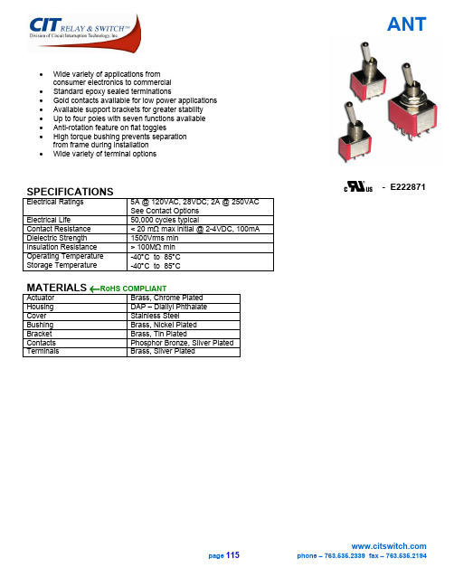
•Wide variety of applications fromconsumer electronics to commercial•Standard epoxy sealed terminations•Gold contacts available for low power applications•Available support brackets for greater stability•Up to four poles with seven functions available•Anti-rotation feature on flat toggles•High torque bushing prevents separationfrom frame during installation•Wide variety of terminal optionsSPECIFICATIONSElectrical Ratings 5A @ 120VAC, 28VDC; 2A @ 250VACSee Contact OptionsElectrical Life 50,000 cycles typicalContact Resistance < 20 mΩ max initial @ 2-4VDC, 100mA Dielectric Strength 1500Vrms minInsulation Resistance > 100MΩ minOperating Temperature Storage Temperature -40°C to 85°C -40°C to 85°CMATERIALS←RoHS COMPLIANTActuatorBrass, Chrome PlatedHousing DAP – Diallyl PhthalateCover StainlessSteel Bushing Brass, Nickel PlatedBracket Brass, Tin PlatedContacts Phosphor Bronze, Silver Plated Terminals Brass, Silver Plated - E222871TOGGLE SWITCH ORDERING INFORMATIONSeries: ANTANT2Number of Poles:1 = SPDT2 = DPDT3 = 3PDT4 = 4PDT3Switch Function:1 = ON-NONE-ON2 = ON-NONE-(ON)3 = ON-OFF-ON4 = (ON)-OFF-(ON)5 = ON-OFF-(ON)6 = ON-ON-ON ** See Three Way Wiring Section for DetailsTActuator:T = 5.08mm, StdS = 10.41mm, StdX = 13.97mm, StdV = 16.26mm, StdW = 21.34mm, StdY = 6.35mm, Flat Toggle **only available with AR1/AR2/AN1/AN2 bushingsF = 12.30mm, Flat Toggle **only available with AR1/AR2/AN1/AN2 bushingsG = 21.00mm, Flat Toggle **only available with AR1/AR2/AN1/AN2 bushingsK = 13.50mm, Flat Toggle **only available with AR1/AR2/AN1/AN2 bushingsZ = 12.37mm, Large Toggle **only available with BZ/BZR bushingsZ1 = 17.45mm, Large Toggle **only available with BZ/BZR bushingsLK = 14.73mm, Locking Toggle, Round Top **only available with K/K1 bushingsLK1 = 14.73mm, Locking Toggle, Flat Top **only available with K/K1 bushingsP(color) = 21.34mm, Plastic **See color choices in Actuator Option sectionPX = 26.30mm, Plastic, Flat Toggle **only available with BZ/BZR bushingsMBushing:E / E1 = 8.89mm, ¼-40NS / Non-Threaded, KeywayF / F1 = 7.10mm, ¼-40NS / Non-Threaded, KeywayJ = 8.89mm, ¼-40NS, FlatW = 8.89mm, M6P-0.75 (Metric), KeywayH = 8.00mm, High Torque, ¼-40NS, KeywayG = 7.52mm, High Torque, ¼-40NS, FlatAR1 / AR2 = 7.55mm, Anti-Rotation, ¼-40NS / Non-Threaded, KeywayAN1 / AN2 = 7.55mm, Anti-Rotation, ¼-40NS / Non-Threaded, FlatBZ = 11.38mm, 15/32 -32NS, KeywayBZR = 11.38mm, 15/32 -32NS, Keyway, with support insertL = 7.55mm, ¼-40NS, Flat, Splash proofK / K1 = 8.00mm, ¼-40NS / Non-Threaded, Keyway**See Actuator Option section for bushing availability with various actuatorsBTerminals:B = Solder Lug,C = PC Pin **Wire wrap terminals available in various lengths, contact factoryD = Quick ConnectH = Horizontal Mount, Right Angle PC Pin; HS = Snap-inV = Vertical Mount, Right Angle PC Pin; VS = Snap-inS20 or S25 = PC Pin with Support Bracket; V20 or V25= Snap-in Support BracketS35 or S40 = PC Pin with Support Bracket; V35 or V40 = Snap-in Support BracketQContacts:Q = Silver PlatedR = Gold PlatedG = Gold over Silver PlatedE Epoxy Seal: E = Epoxy SealActuator Cover:Blank = No CoverS = for S, T, X, V, & W actuators E = for E, F, J, & G bushingsZ = for BZ & BZR bushingsActuator Cover Colors:1 = White2 = Black3 = Red** Color choices only available with S toggle coverSWITCH FUNCTIONToggle PositionFunction1 ON NONE ON2 ON NONE (ON)3 ON OFF ON SPDT4 (ON) OFF (ON)5 ON OFF (ON)Terminals2-3 --- 2-1Toggle PositionFunction1 ON NONE ON2 ON NONE (ON)3 ON OFF ON4 (ON) OFF (ON)5 ON OFF (ON) DPDT Terminals2-35-6--- 2-15-46 ON ON ONTerminals2-35-62-35-42-15-4Toggle PositionFunction1 ON NONE ON2 ON NONE (ON)3 ON OFF ON 3PDT4 (ON) OFF (ON)5 ON OFF (ON)Terminals2-35-68-9---2-15-48-7Toggle PositionFunction1 ON NONE ON2 ON NONE (ON)3 ON OFF ON4 (ON) OFF (ON)5 ON OFF (ON) 4PDT Terminals2-35-68-911-12---2-15-48-711-106 ON ON ONTerminals2-35-68-911-122-35-48-911-102-15-48-711-10ACTUATOR OPTIONS** Actuator lengths shown with E bushing, subtract 1.78mm for F/F1 bushing, subtract 0.51mm for M bushingT S X VW** Only available with AR1/AR2 & AN1/AN2 bushings.Y F G K** Only available with BZ & BZR bushings.Z Z1 PXPX actuator is plastic (Black)** LK & LK1 only available with K & K1 bushings. LK & LK1 are not available with momentary functions** P actuator is plastic P2 = Black, std P1 = White P3 = RedContact factory for other color optionsLK LK1 P2BUSHING OPTIONSE (Threaded)E1 (Non-Threaded)F (Threaded)F1 (Non-Threaded)J (Threaded) H (Threaded)High TorqueG (Threaded)High TorqueW (Threaded)MetricAR1 (Threaded)AR2 (Non-Threaded)Anti-RotationAN1 (Threaded)AN2 (Non-Threaded)Anti-RotationBZ (Threaded) BZR (Threaded)Impact ResistantK (Threaded)K1 (Non-Threaded)** If selecting F, G, or K actuator, one of thesebushings must be selected** Only used with Z, Z1, & PX actuators **Only used with LK & LK1actuatorsPANEL MOUNTING1/4”- 40 Bushings Metric Bushing15/32” BushingsL (Threaded)Splash Proof** Not available withZ, Z1, & PX actuatorsTERMINAL OPTIONSB (Single Pole)B (Double Pole)B (3 Pole)B (4 Pole)C (Single Pole)C (Double Pole)C (3 Pole)C (4 Pole)D (Single Pole)D (Double Pole) D (3 Pole) D (4 Pole)H (HS – Snap-in) = Horizontal Mount, Right Angle PC Pins (Single Pole)H (HS – Snap-in) = Horizontal Mount, Right Angle PC Pins (Double Pole)TERMINAL OPTIONSV (VS – Snap-in) = Vertical Mount, Right Angle PC Pins (Single Pole)V (VS – Snap-in) = Vertical Mount, Right Angle PC Pins (Double Pole)V (VS – Snap-in) = Vertical Mount, Right Angle PC Pins (Three Pole)V (VS – Snap-in) = Vertical Mount, Right Angle PC Pins (Four Pole)TERMINAL OPTIONSTerminal Option “A”Dimension S20-V20 11.68S25-V25 16.00S20/S25 (V20/V25 – Snap-in Bracket) = PC Pins with Support Bracket (Single Pole)Terminal Option “A”Dimension S20-V20 11.68 S25-V25 16.00S20/S25 (V20/V25 – Snap-in Bracket) = PC Pins with Support Bracket (Double Pole)Terminal Option “A”Dimension S20-V20 11.68 S25-V25 16.00S20/S25 (V20/V25 – Snap-in Bracket) = PC Pins with Support Bracket (Three Pole)TERMINAL OPTIONSTerminal Option“A” DimensionS20-V20 11.68S25-V25 16.00 S20/S25 (V20/V25 – Snap-in Bracket) = PC Pins with Support Bracket (Four Pole)Terminal Option“A” DimensionS35-V35 11.68S40-V40 16.00 S40 (V40 – Snap-in Bracket) = PC Pins with Support Bracket (Single Pole)Terminal Option“A” DimensionS35-V35 11.68S40-V40 16.00 S40 (V40 – Snap-in Bracket) = PC Pins with Support Bracket (Double Pole)TERMINAL OPTIONSTerminal Option “A”Dimension S35-V35 11.68S40-V40 16.00S40 (V40 – Snap-in Bracket) = PC Pins with Support Bracket (Three Pole)Terminal Option “A”Dimension S35-V35 11.68S40-V40 16.00S40 (V40 – Snap-in Bracket) = PC Pins with Support Bracket (Four Pole)CONTACT OPTIONSDesignator Contact MaterialTerminal MaterialElectrical RatingsQSilver PlatingSilver Plating5A @ 120VAC, 28VDC; 2A @ 250VAC R Gold over Nickel Plating Gold over Nickel Plating .4 VA max @ 20VAC or VDC max GGold over Silver PlatingGold over Silver Plating.4 VA max @ 20VAC or VDC max or 5A @ 120VAC, 28VDC; 2A @ 250VACCAP OPTIONSRUBBER TOGGLE COVERS_SEALED BOOTESEALED BOOTZ** For use with S, T, X, V, & W actuators1 = White,2 = Black,3 = Red** For use with E, F, J, & G bushings only.Black color standard.** For use with BZ & BZR bushings only. Blackcolor standard.page 125phone – 763.535.2339 fax – 763.535.2194THREE WAY WIRING DIAGRAMPOSITION 1POSITION 2POSITION 3POSITION 1POSITION 2POSITION 3HARDWARE**Two hex nuts, one lock washer, & one locking ring supplied standard with threaded bushingsHex NutLock WasherLocking RingDress NutKnurled NutKnurled Nut**For use with E, F, M, AR1, L, & K bushingsHex Nut Lock WasherLocking RingDress NutKnurled NutKnurled Nut**For use with J, G, & AN1 bushingsHex Nut Lock WasherLocking Ring**For use with BZ & BZR bushingsANT元器件交易网。
3级英语考试1600个词组、单词(带中文)打印版

Aability n. 能力;才能able a. 能够;有能力的about ad. 大约;到处;四处prep. 关于;在各处;四处above prep. 在……上面abroad ad. 到(在)国外absent a. 缺席,不在accent n. 口音,音调accept vt. 接受accident n. 事故,意外的事ache vi.& n. 痛,疼痛achieve vt. 达到,取得across prep. 横过,穿过act n. 法令,条例v. (戏)表演,扮演(角色),演出(戏);行动,做事action n. 行动active a. 积极的,主动的activity n. 活动add vt. 添加,增加address n. 地址advantage n. 优点;好处advertisement n. 广告advice n. 忠告,劝告,建议advise vt. 忠告,劝告,建议afford vt. 负担得起(……的费用);抽得出(时间);提供afraid a. 害怕的;担心after ad. 在后;后来prep. 在……之后;在……后面conj. 在……以后afternoon n. 下午,午后again ad. 再一次;再,又against prep. 对着,反对age n. 年龄;时代ago ad. 以前agree v. 同意;应允agreement n. 同意,一致;协定,协议air n. 空气;大气airline n. 航空公司;航空系统airplane n. (美)飞机airport n. 航空站,飞机场alive a. 活着的,存在的all ad. 全部地pron. 全部;全体人员allow vt. 允许,准许almost ad. 几乎,差不多alone a. 单独的,孤独的along ad. 向前;和……一起;一同prep. 沿着;顺着aloud ad. 大声地already ad. 已经also ad. 也although conj. 虽然,尽管always ad. 总是;一直;永远America * n. 美国;美洲American a. 美国的;美国人的n. 美国人among prep. 在……中间;在(三个以上)之间amuse vt. (使人)快乐,逗乐ancient a. 古代的,古老的and conj. 和;又;而angry a. 生气的,愤怒的animal n. 动物another a. 再一;另一;别的;不同的pron. 另一个answer n. 回答,答复;回信;答案v. 回答,答复;回信;(作出)答案ant n. 蚂蚁any pron. (无论)哪一个;哪些任何的;(用于疑问句、否定句)一些;什么anybody pron. 任何人,无论谁anyone pron. 任何人,无论谁anything pron. 什么事(物);任何事(物)anyway ad. 不管怎样anywhere ad. 任何地方appear vi. 出现apple n. 苹果April n. 4 月area n. 面积;地域,地方,区域;范围,领域arm n. 臂, 支架army n. 军队around ad. 在周围;在附近prep. 在……周围;大约arrive vi. 到达;达到article n. 文章;东西;冠词art n. 艺术,美术;技艺as ad.& conj.像……一样;如同;因为prep. 作为,当做Asia * n. 亚洲Asian a. 亚洲的,亚洲人的n.亚洲人ask v. 问,询问;请求,要求;邀请asleep a. 睡着的,熟睡at prep. 在(几点钟);在(某处)Atlantic a. 大西洋的attention n. 注意,关心August n. 8 月aunt n. 舅母;婶;姑;姨Australia * n. 澳洲;澳大利亚Australian a. 澳洲的,澳大利亚人的n. 澳大利亚人autumn n. 秋天,秋季avoid v. 避免,躲开,逃避awake (awoke, awo ken) v.唤醒醒着的away ad. 离开;远离Bbaby n. 婴儿back ad. 回(原处);向后a.后面的background n. 背景bad ( 比较级worse, 最高级worst) a. 坏的;有害的,不利的;严重的balloon n. 气球bamboo n. 竹banana n. 香蕉bank n. (河、海、湖的)岸,堤银行baseball n. 棒球basic a. 基本的basket n. 篮子basketball n. 篮球bathroom n. 浴室,盥洗室1be v. 是(原形),其人称和时态形式有am, is, are, was, were, being, been ;成为beach n. 海滨,海滩bear n. 熊beat (beat, beaten) v. 敲打;跳动;打赢n. (音乐)节拍beautiful a. 美的,美丽的,美观的because conj. 因为become (became, become) v. 变得;成为bed n. 床bedroom n. 寝室,卧室bee n.. 蜜蜂beef n. 牛肉before prep. 在……以前;在……前面ad. 以前conj. 在……之前begin(began,begun)v. 开始,着手behaviour n. 行为,举止behind prep. ( 表示位置) 在……后面ad. 在后面;向后believe v. 相信,认为bell n. 钟,铃;钟( 铃) 声;钟形物below prep. 在……下面belt n. (皮)带beside prep. 在……旁边;靠近besides prep. 除……以外(还有)ad. 还有,此外between prep. 在(两者)之间;在……中间beyond prep. ( 表示位置) 在……的那边big a. 大的bike = bicycle n. 自行车bill n. 账单;法案,议案;(美)钞票,纸币bird n. 鸟birth n. 出生;诞生birthday n. 生日biscuit n. 饼干bit n. 一点,一些,少量的bitter a. 有苦味的;痛苦的,难过的;严酷的black n. 黑色a. 黑色的blackboard n. 黑板blind a. 瞎的blood n. 血,血液blow n. 击;打击blue n. 蓝色 a. 蓝色的悲伤的;沮丧的board n. 木板;布告牌;委员会;(政府的)部v. 上(船、火车、飞机)boat n. 小船,小舟body n. 身体book n. 书;本子v. 预定,定(房间、车票等)boring a. 乏味的,无聊的born a. 出生borrow v. (向别人)借用;借boss n. 领班;老板both a. 两;双pron. 两者;双方bottle n. 瓶子bottom n. 底部;底bowl n. 碗box n. 盒子,箱子boy n. 男孩brain n. 脑(子)brave a. 勇敢的bread n. 面包break (broke, broken) v. 打破(断,碎);损坏,撕开n. 间隙breakfast n. 早餐breath n. 气息;呼吸breathe vi. 呼吸bridge n. 桥bright a. 明亮的;聪明的bring (brought, brought) vt.拿来,带来,取来brother n. 兄;弟brown n. 褐色,棕色a. 褐色的,棕色的brush v. 刷;擦n. 刷子build (built, built) v. 建筑;造building n. 建筑物;房屋;大楼bun n. 馒头;小甜面包burn (-ed, -ed 或burnt,burnt) v. 燃,烧,着火;使烧焦;使晒黑n. 烧伤;晒伤bus n. 公共汽车business n. (本分)工作,职业;职责;生意,交易;事业busy a. 忙(碌)的but conj. 但是,可是prep. 除了,除……外butter n. 黄油,奶油butterfly n. 蝴蝶buy(bought,bought)vt. 买by prep. 靠近,在……旁;在……时间;不迟于;被;用;由;乘(车)bye int. 再见Ccabbage n. 卷心菜,洋白菜cake n. 蛋糕,糕点;饼call n. 喊,叫;电话,通话v.称呼;呼唤;喊,叫camel n. 骆驼camera n. 照相机;摄像机camp n. (夏令)营vi. 野营;宿营Canada * n. 加拿大cancel vt. 取消cancer n. 癌candle n. 蜡烛candy n. 糖果cap n. (无檐的或仅在前面有檐的)帽子;(瓶子的)盖;(钢笔等的)笔套capital n. 首都,省会;大写;资本captain n. (海军)上校;船长,舰长;队长care n. 照料,保护;小心v.介意……,在乎;关心careful a. 小心的,仔细的,谨慎的careless a. 粗心的,漫不经心的2carry vt. 拿,搬,带,提,抬,背,抱,运等cat n. 猫]catch(caught,caught)v. 接住;捉住;赶上;染上(疾病)cause n. 原因,起因vt. 促使,引起,使发生CD ROM 信息储存光盘(compact disk read only memory 的缩写)ceiling n. 天花板,顶棚celebrate v. 庆祝cent n. 美分(100 cents = 1 dollar )centre ( 美center ) n. 中心,中央century n. 世纪,百年certain a. (未指明真实名称的)某……;确定的,无疑的;一定会……chair n. 椅子chairman n. 主席,会长;议长chairwoman n. 女主席, 女会长;女议长chalk n. 粉笔chance n. 机会,可能性change n. 零钱;找头v. 改变,变化;更换;兑换cheap a. 便宜的,贱cheat n. & v. 骗取,哄骗;作弊check n. 检查;批改vt. 校对,核对;检查;批改cheer n. & vi.欢呼;喝彩cheese n. 奶酪chemistry n. 化学chess n. 棋chest n. 箱子;盒子;胸部chicken n. 鸡;鸡肉child ( 复children) n. 孩子,China * n. 中国Chinese a. 中国的;中国人的;中国话的,汉语的n. 中国人;中国话,汉语,中文chocolate n. 巧克力choice n. 选择;抉择choose (chose, cho sen) vt.选择chopsticks n. 筷子Christmas n. 圣诞节(12 月25 日)church n. 教堂;教会cinema n. 电影院;电影circle n. vt. 圆圈将…圈起来city n. 市,城市,都市clap vi. 拍手;鼓掌class n. (学校里的)班;年级;课classmate n. 同班同学classroom n. 教室clean vt. 弄干净,擦干净 a.清洁的,干净的clear a. 清晰的;明亮的;清楚的clever a. 聪明的,伶俐的climb v. 爬,攀登clock n. 钟clone n.克隆(无性繁殖出来的有机体群)close 1 a . 亲密的;近,靠近ad. 近,靠近close 2 vt. 关,关闭cloth n.布clothes n. 衣服;各种衣物cloud n. 云;云状物;阴影cloudy a. 多云的,阴天的club n. 俱乐部;纸牌中的梅花coach n. 教练;马车;长途车coal n. 煤;煤块coast n. 海岸;海滨coat n. 外套;涂层;表皮;皮毛vt. 给……穿外套;涂上coffee n. 咖啡coin n. 硬币Coke n. 可口可乐cold a. 冷的,寒的n. 寒冷;感冒,伤风collect vt. 收集,搜集college n. 学院;专科学校colour ( 美color) n. 颜色vt.给……着色,涂色come (came, come) vi. 来,来到comfortable a. 舒服的;安逸的;舒服自在的common a. 普通的,一般的;共有的communicate v. 交际;传达(感情,信息等)communication n. 交际;交往;通讯company n. 公司compare vt. 比较,对照competition n. 比赛,竞赛complete a. 完成的vt. 完成,结束composition n. 作文;作曲computer n. 电子计算机concert n. 音乐会;演奏会condition n. 条件,状况conference n. (正式的)会议;讨论connect vt. 连接,把……联系起来consider vt. 考虑continue vi. 继续control vt.& n. 控制conversation n. 谈话,交谈cook n. 炊事员,厨师v. 烹调,做饭cooker n. 炊具( 锅、炉灶、烤炉等)cool a. 凉的,凉爽的;酷copy n. 抄本,副本;一本(份,册……)v. 抄写;复印;(计算机用语)拷(备份盘)corner n. 角;角落;拐角correct v. 改正;纠正a. 正确的,对的;恰当的cost (cost, cost) v. 值(多少钱);花费; n. 价格cotton n. 棉花a. 棉花的cough n.& vi. 咳嗽could modal v.(can的过去式)可以……;(表示许可或请求)可以……,3行count vt. 数,点数country n. 国家;农村,乡下countryside n. 乡下,农村couple n. 夫妇,一对courage n. 勇气;胆略course n. 过程;经过;课程cousin n. 堂(表)兄弟,堂(表)姐妹cover n. 盖子;罩v. 覆盖,遮盖;掩盖cow n. 母牛,奶牛crayon n 蜡笔;蜡笔画crazy a. 疯狂的create vt. 创造;造成cross n. 十字形的东西vt. 越过;穿过cruel a. 残忍的,残酷的;无情的cry n. 叫喊;哭声v. 喊叫;哭culture n. 文化cup n. 茶杯cut (cut, cut) v. n. 切,剪,削,割伤口Ddad = daddy n. (口语)爸爸,爹爹daily a. 每日的;日常的ad. 每天n. 日报dance n.& vi. 跳舞danger n. 危险dangerous a. 危险的dare v.& aux.(后接不带to 的不定式;主要用于疑问,否定或条件句)敢,敢于dark n. 黑暗;暗处;日暮a. 黑暗的;暗淡的;深色的date n. 日期;约会daughter n. 女儿day n. (一)天,(一)日;白天dead a. 死的;无生命的deaf a. 聋的deal n. 量,数额;交易dear a . 亲爱的;贵的death n. 死December n. 12 月decide v. 决定;下决心decision n. 决定;决心deep a. 深ad. 深;深厚degree n. 程度;度数;学位delicious a. 美味的,可口的dentist n. 牙科医生depend vi. 依靠,依赖,指望;取决于describe vt. 描写,叙述desk n. 书桌,写字台develop v. (使)发展;(使)发达;(使)发育;开发vt. 冲洗(照片)development n. 发展,发达,发育,开发dialogue ( 美dialog) n. 对话diary n. 日记;日记簿dictionary n. 词典,字典difference n. 不同different a. 不同的,有差异的difficult a. 难的;艰难的;不易相处的difficulty n. 困难,费力dig (dug, dug) v. 挖(洞、沟等);掘dinner n. 正餐,宴会direct a. vt. 直接的;直达的;直截了当的指挥;指导;监督;管理;指挥(演奏);导演(电影)direction n. 方向;方位director n. 所长,处长,主任;董事;导演dirty a. 脏的discover vt. 发现discovery n. 发现discuss vt. 讨论,议论discussion n. 讨论,辩论disease n. 病,疾病dish n. 盘,碟;盘装菜;盘形物dismiss vt. 让……离开;遣散;解散;解雇disturb vt. 扰乱;打扰divide vt. 分,划分do (did, done) don't=do notv. & aux.做,干(用以构成疑问句及否定句。
Heat treatmant中英文术语对照

热处理术语中文名称英文名称说明1. 整体热处理{ Bulk heat treatment}[bʌlk]: 对金属材料或工件进行穿透加热的热处理工艺。
2. 局部热处理{Local heat treatment}:仅对工件的某一部位或几个部位进行热处理的工艺。
3. 表面热处理{Surface heat treatment}:仅对工件表层进行热处理以改变其组织和性能的工艺。
4.化学热处理{ Thermo-chemical treatment} ['θə:məu] ( adj. 热的;热电的):把金属材料或工件放在适当的活性介质中加热、保持,使一种或几种化学元素渗入其表层,以改变其化学成分、组织和性能的热处理工艺。
5.预备热处理(Conditioning heat treatment):为了调整原始组织,以保证工件最终热处理或(和)可加工性能,在最终热处理前预先进行的热处理。
6.可控气氛热处理{Heat treatmen in-controlled atmosphere}:为达到无氧化、无脱碳、按要求增碳的目的,在成分可以控制的炉气中进行加热和冷却的热处理工艺。
7. 真空热处理{Vacuum heat treatment} ['vækjuəm]:在一定真空度的加热炉中,可实现工件无氧化的热处理工艺。
8.离子热处理{Ion heat treatment}['aiən]: 在一定真空度的特定气氛中,利用工件(阴极)和阳极之间等离子体的辉光放电进行热处理的技术。
9. 高能束热处理{High energy density heat treatment}:利用激光、电子束、等离子弧、感应脉冲、涡流、火焰等高功率密度能源加热工件的热处理技术。
10.奥氏体化{Austenitizing} ['ɔstinitaiz, 'ɔstəni,taiz]:将钢铁加热至Ac3或Ac1以上,使原始组织全部或部分转变为奥氏体的工艺。
电路图中常用的英文缩写的中文解释
AA 模拟A/DC模拟信号到数字信号的转换A/L音频/逻辑板AAFPCB音频电路板AB 地址总线ab 地址总线accessorier 配件ACCESSORRIER 配件ADC(A/O)模拟到数字的转换adc 模拟到数字的转换ADDRESS BUS地址总线AFC 自动频率控制afc 自动频率控制AFC自动频率控制AFMS 来音频信号afms 来自音频信号AFMS来音频信号AFPCB 音频电路板AF音频信号AGC 自动增益控制agc 自动增益控制AGC自动增益控制aged 模拟地AGND 模拟地AGND模拟地ALARM 告警alarm 告警ALC 自动电平控制ALEV 自动电平AM 调幅AMP 放大器AMP放大器AM调幅ANT 天线ANT/SW 天线开关ant 天线Anternna天线antsw 天线开关ANTSW天线切换开关ANT天线APC 自动功率控制APC/AOC自动功率控制ARFCH 绝对信道号ASIC 专用接口集成电路AST-DET 饱和度检测ATMS 到移动台音频信号atms 到移动台音频信号ATMS到移动台音频信号AUC 身份鉴定中心AUDIO 音频AUDIO音频AUTO自动AUX辅助AVCC音频处理芯片A模拟信号b+ 内电路工作电压BALUN平衡于一不平衡转换BAND-SEL频段选择/切换BAND频段Base band基带(信号)base 三极管基极batt+ 电池电压BDR接收数据信号Blick Diagram方框图BPF带通滤波器BUFFER缓冲放大器BUS通信总线buzz 蜂鸣器CCALL 呼叫CARD 卡Carrier载波调制CCONTCSX开机维持(NOKIA) CCONTINT关机请求信号CDMA 码分多址cdma 码分多址CEPT 欧洲邮电管理委员会CH 信道CHAGCER 充电器CHECK 检查CIRCCITY 整机Circuit Diagram电路原理图CLK 时钟CLK-OUT逻辑时钟输出CLK-SELECT时钟选择信号(Motorola 手机)COBBA音频IC(诺基亚系列常用)COL 列COLLECTOR 集电极CONTROL 控制control 控制CP 脉冲、泵CP-TX RXVCO控制输出接收锁相电平CP-TX TXVCO控制输出发射锁相电平CPU 中央处理器cpu 中央处理器CS 片选CTL-GSM频段控制信号d b 数据总线D/AC数字信号到模拟信号的转换d 数字dac 数字到模拟的转换dcin 外接直流电愿输入DCS-CS发射机控制信号:控制TXVCO与I/Q调制器DDI数据接口电路DECIPHRIG解秘DEINTERLEARING去交织DET检测dfms 来数据信号dgnd 数字地Diplex双工滤波器Direct Coner Siorl Lionear Receicer直接变换的线性接收机dsp 数字信号处理器DSP数字信号处理器dtms 到数据信号DUPLEX / DIPLEX双工器Duplex Sapatation双工间隔EEarph 耳机EEPROM 电擦除可编程只读存储器EIR 设备号寄存器EL 发光EMITTER 发射极emitter 三极管发射极EMOD Demodu Laticon解调EN 使能EN 使能、允许、启动en 使能ENAB 使能EPROM 电编程只读存贮器ERASABLE 可擦的ETACS 增强的全接入通信系统etacs 增强的全接入通信系统EXT 外部EXT 外部ext 外部的FBUS处接通信接口信号线fdma 频分多址feed back 反馈fh 跳频FILFTER滤波器fl 滤波器fm 调频from 来自于gain 增益GAIN增益Gen Out信号发生器gnd 地GSM-PINDIODE功率放大器输出匹配电路切换控制信号GSM-SEL频段切换控制信号之一G-TX-VCO900MHZ发射VCO切换控制hook 外接免提状态II 同相支路I/O 输入/输出I/O输入/输出i/o输入输出i 同相支路IC 集成电路ICTRL 供电电流大小控制端ictrl 供电电流大小控制端IF 中频if 中频IFLO中频本振IF中频IMEI 国际移动设备识别码IN 输入INSERT CARD 插卡INT 中断int 中断Interface界面,电子电路基础知识2,接口ISDN 综合业务数字网I同相支路LayoutPCB元件分布图LCDCLK显示器时钟led 发光二极管LOCK锁定loop fliter 环路滤波器LO本振LPF低通滤波器lspctrl 扬声器控制MMAINVCO主振荡器(Motorola) MCC 移动国家码MCLK 主时钟mclk 主时钟MCLK主时钟MCLK主时钟MDM 调制解调MDM调制解调器(Motorola手机) MENU 菜单MF 陶瓷滤波器MIC 话筒mic 送话器MISO主机输入从机输出(Motorola) MIX 混合Mixed Second第二混频信号MIXER SECOND 第二混频信号MIX混频器MOD 调制信号mod 调制信号MODEM调制解调器MODFreq调制频率MODIN 调制I信号负modin 调制i信号负MODIN调制I信号负MODIP 调制I信号正MODIP调制I信号正MODQN 调制Q信号负MODQN调制Q信号负MODQP 调制Q信号正MODQP调制Q信号正MOD调制MOD调制信号MOEM调制解调器DM mopip 调制i信号正MOSI主机输出从机输入(Motorola) MS 移动台MSC 移动交换中心MSIN 移动台识别码MSK 最小移频键控MSRN 漫游MUTE 静音mute 静音NNAM 号码分配模块NC 空、不接NO NETWORK 无网络ofst 偏置on 开onsrq 免提开关控制PA 功率放大器PADRV功率放大器驱动PCB板图PCM脉冲编码调制PD/PH相位比较器pll 锁相环PLL锁相环PLL锁相环路powcontrol 功率控制POWCONTROL功率控制Power Supply电源系统powlev 功率级别POWLEV功放级别PURX复位信号(NOKIA)pwrsrc 供电选择QQ uadrature modulalion正交调制Q 正交支路Q 正交支路q 正交支路RRACH 随机接入信道RADIO射频本振RAM 随机存储器ram 随机储存器(暂存)RD 读Receiver收信机REF 参考、基准ref 参考RESET 复位reset 复位RF PCB 射频板RF 射频rf 射频RFADAT 射频频率合成器数据rfadat 射频频率合成数据RFADAT射频频率合成器数据RFAENB 射频频率合成器启动rfaenb 射频频率合成启动RFAENB射频频率合成器启动RFConnector射频接口RFI 射频接口RFIN/OFF高频输入/输出ROM 只读存储器ROW 行RSSI 场强RSSI 接收信号强度指示rssi 接收强度指示RSSI接收信号强度指示RX 接收rx 接收RX-ACQ接收机数据传输请求信号RXEN接收使能RXIFN 接收中频信号负rxifn 接收中频信号负RXIFN接收中频信号负RXIFP 接收中频信号正rxifp 接收中频信号正RXIFP接收中频信号正RXIN接收I信号负RXIN接收输出RXIP接收I信号正RXI接收基带信号(同相) RXON 接收开rxon 接收开RXON接收机启动/开关控制RXOUT接收输出RXQN接收Q信号负RXQP接收Q信号正RXQ接收基带信号(正交) RXVCO 收信压控振荡器RX接收sat-det 饱和度检测saw 声表面波滤波器SAW声表面波滤波器SF超级滤波器SHFVCO专用射频VCO(NOKIA) SLEEPCLK睡眠时钟SMOC数字信号处理器spi 串行外围接口spk 扬声器SUPLEX双工器作用相当于天线开关sw 开关swdc 末调整电压SW开关synclk 频率合成器时钟SYNCLK频率合成器时钟syndat 频率合成器数据SYNDAT频率合成器数据SYNEN频率合成器启动/使能synstr 频率合成器启动SYNSTR频率合成器启动SYNTCON频率合成器开/关synton 频率合成器开/关TTACS 全接入移动通信系统TCH 话音通道TDMA 时分多址tdma 时分多址TEMP 温度监测temp 温度监测TEST 测试TP 测试点tp 测试点 tx 发送Transmitter发信机TRX 收发信机TX EN 发送使能tx en 发送使能TX 发送TX 发信TXC 发信控制TX-DEY-OUT发射时序控制输出TXENT发射供电TXEN发射使能TXEN发送使能TX-IF 发信中频TXIN发送I信号负TXIP发送I信号正TXI发射基带信号TXON 发送开txon 发送开TXON发送开TXOUT发射输出TXPWR发射功率TXQN发送Q信号负TXQP发送Q信号正TXQ发射基带信号TXRF发射射频TXVCO 发信压控振荡器txvco 发送压控振荡器频率控制UHFVCO超高频/射频VCOUHF超高频段UI用户接口BSIC专用集成电路UREGISTERED未注册vbatt 电池电压vcc 电愿VCO 压控振荡器vco 压控振荡VCTCXO温补压控振荡器vcxocont 基准振荡器频率控制VHFVCO甚高频/中频VCOvpp 峰峰值vppflash flash 编程控制vrpad 调整后电压vswitch 开关电压WWATCH DOG 看门狗WATCHDOG看门狗信号WCDMA 宽带码分多址WD-CP 看门狗脉冲WDG看门狗(维持信号电压) WDOG 看门狗WR 写逻辑音频电路射频电路电路图中常用的英文缩写的中文解释电子知识UHF超高频段UREGISTERED未注册SW开关UI用户接口BSIC专用集成电路BAND频段BAND-SEL频段选择/切换BUFFER缓冲放大器BUS通信总线DET检测Circuit Diagram电路原理图Blick Diagram方框图PCB板图LayoutPCB元件分布图Receiver收信机Transmitter发信机Interface界面,电子电路基础知识2,接口Power Supply电源系统射频电路A模拟信号AFC自动频率控制AGC自动增益控制APC/AOC自动功率控制AGND模拟地ANT天线ANTSW天线切换开关AM调幅BPF带通滤波器CP-TX RXVCO控制输出接收锁相电平CP-TX TXVCO控制输出发射锁相电平DUPLEX / DIPLEX双工器Duplex Sapatation双工间隔DCS-CS发射机控制信号:控制TXVCO与I/Q调制器FILFTER滤波器Gen Out信号发生器GAIN增益GSM-PINDIODE功率放大器输出匹配电路切换控制信号GSM-SEL频段切换控制信号之一G-TX-VCO900MHZ发射VCO切换控制IF中频IFLO中频本振LO本振LOCK锁定MODFreq调制频率Mixed Second第二混频信号PA 功率放大器PLL锁相环路PADRV功率放大器驱动TXRF发射射频TXEN发射使能TXENT发射供电TXIN发送I信号负TXIP发送I信号正TXON发送开TXQN发送Q信号负TXQP发送Q信号正TXI发射基带信号TX-DEY-OUT发射时序控制输出TXQ发射基带信号UHFVCO超高频/射频VCO VHFVCO甚高频/中频VCO SHFVCO专用射频VCO(NOKIA) VCO 压控振荡器VCTCXO温补压控振荡器AMP放大器CTL-GSM频段控制信号Diplex双工滤波器SUPLEX双工器作用相当于天线开关LPF低通滤波器MAINVCO主振荡器(Motorola)MIX混频器Anternna天线RFConnector射频接口BALUN平衡于一不平衡转换Direct Coner Siorl Lionear Receicer 直接变换的线性接收机Carrier载波调制POWCONTROL功率控制POWLEV功放级别RFIN/OFF高频输入/输出RADIO射频本振RFADAT射频频率合成器数据RFAENB射频频率合成器启动RSSI接收信号强度指示RX接收RXIN接收输出RXON接收机启动/开关控制RXOUT接收输出RXEN接收使能RXIFN接收中频信号负RXIFP接收中频信号正RXIN接收I信号负RXIP接收I信号正RXQN接收Q信号负RXQP接收Q信号正RX-ACQ接收机数据传输请求信号RXI接收基带信号(同相)RXQ接收基带信号(正交)SAW声表面波滤波器SF超级滤波器SYNCLK频率合成器时钟SYNDAT频率合成器数据SYNEN频率合成器启动/使能SYNSTR频率合成器启动SYNTCON频率合成器开/关TX 发送TXEN发送使能TXOUT发射输出TXPWR发射功率逻辑音频电路AFMS来音频信号AAFPCB音频电路板ATMS到移动台音频信号AUDIO音频AUX辅助AVCC音频处理芯片AUTO自动A/L音频/逻辑板COBBA音频IC(诺基亚系列常用) Base band基带(信号)BDR接收数据信号CLK-OUT逻辑时钟输出CLK-SELECT时钟选择信号(Motorola手机) DEINTERLEARING去交织DECIPHRIG解秘I同相支路I/O输入/输出MODEM调制解调器MCLK主时钟MDM调制解调器(Motorola手机) MISO主机输入从机输出(Motorola) MOD调制信号MODIN调制I信号负MODIP调制I信号正MODQN调制Q信号负MODQP调制Q信号正MOSI主机输出从机输入(Motorola) PCM脉冲编码调制Q uadrature modulalion正交调制Q 正交支路SMOC数字信号处理器WATCHDOG看门狗信号WDG看门狗(维持信号电压)A/DC模拟信号到数字信号的转换AF音频信号CCONTCSX开机维持(NOKIA) CCONTINT关机请求信号D/AC数字信号到模拟信号的转换DDI数据接口电路EMOD Demodu Laticon解调DSP数字信号处理器FBUS处接通信接口信号线MCLK主时钟MOD调制MOEM调制解调器DMPD/PH相位比较器PLL锁相环PURX复位信号(NOKIA) SLEEPCLK睡眠时钟LCDCLK显示器时钟ab》地址总线accessorier》配件adc》模拟到数字的转换afc》自动频率控制agc》自动增益控制aged》模拟地afms》来自音频信号alarm》告警ant》天线antsw》天线开关atms》到移动台音频信号base》三极管基极batt+》电池电压b+》内电路工作电压buzz》蜂鸣器cdma》码分多址control》控制cpu》中央处理器d》数字dac》数字到模拟的转换d b》数据总线dcin》外接直流电愿输入dgnd》数字地dtms》到数据信号dfms》来数据信号dsp》数字信号处理器emitter》三极管发射极en》使能etacs》增强的全接入通信系统ext》外部的feed back》反馈fdma》频分多址fh》跳频fl》滤波器fm》调频from》来自于gain》增益gnd》地hook》外接免提状态i》同相支路if》中频int》中断i/o输入输出ictrl》供电电流大小控制端led》发光二极管loop fliter》环路滤波器lspctrl》扬声器控制mclk》主时钟mic》送话器mod》调制信号mopip》调制i信号正modin》调制i信号负mute》静音ofst》偏置on》开onsrq》免提开关控制powcontrol》功率控制powlev》功率级别pwrsrc》供电选择pll》锁相环q》正交支路ram》随机储存器(暂存)ref》参考reset》复位rf》射频rfadat》射频频率合成数据rfaenb》射频频率合成启动rssi》接收强度指示rx》接收rxon》接收开rxifp》接收中频信号正rxifn》接收中频信号负sat-det》饱和度检测saw》声表面波滤波器spk》扬声器spi》串行外围接口swdc》末调整电压synstr》频率合成器启动synclk》频率合成器时钟syndat》频率合成器数据synton》频率合成器开/关sw》开关tdma》时分多址temp》温度监测txvco》发送压控振荡器频率控制tp》测试点tx》发送tx en》发送使能txon》发送开vbatt》电池电压vrpad》调整后电压vpp》峰峰值vppflash flash》编程控制vcxocont》基准振荡器频率控制vswitch》开关电压vcc》电愿vco》压控振荡AA模拟AB地址总线ACCESSORRIER配件ADC(A/O)模拟到数字的转换ADDRESS BUS地址总线AFC自动频率控制AGC自动增益控制AGND模拟地AFMS来音频信号ALARM告警ALEV自动电平ALC自动电平控制AM调幅AMP放大器ANT天线ANT/SW天线开关APC自动功率控制ARFCH绝对信道号AFPCB音频电路板ATMS到移动台音频信号ASIC专用接口集成电路AST-DET饱和度检测AUC身份鉴定中心AUDIO音频CCDMA码分多址CONTROL控制CPU中央处理器CIRCCITY整机COLLECTOR集电极CALL呼叫CARD卡CEPT欧洲邮电管理委员会CH信道CHAGCER充电器CHECK检查CLK时钟COL列CP脉冲、泵CS片选EEMITTER发射极EN使能ENAB使能ETACS增强的全接入通信系统EXT外部EL发光ERASABLE可擦的Earph耳机EEPROM电擦除可编程只读存储器EPROM电编程只读存贮器EIR设备号寄存器EN使能、允许、启动EXT外部II同相支路IF中频INT中断I/O输入/输出ICTRL供电电流大小控制端IC集成电路IMEI国际移动设备识别码IN输入INSERT CARD插卡ISDN综合业务数字网MMCLK主时钟MIC话筒MOD调制信号MODIP调制I信号正MODIN调制I信号负MODQP调制Q信号正MODQN调制Q信号负MUTE静音MIXER SECOND第二混频信号MF陶瓷滤波器MCC移动国家码MENU菜单MDM调制解调MIX混合MS移动台MSC移动交换中心MSK最小移频键控MSIN移动台识别码MSRN漫游NNAM号码分配模块NC空、不接NO NETWORK无网络QQ正交支路RRAM随机存储器REF参考、基准RESET复位RF射频RFADAT射频频率合成器数据RFAENB射频频率合成器启动RSSI接收信号强度指示RX接收RXON接收开RXIFP接收中频信号正RXIFN接收中频信号负RF PCB射频板RACH随机接入信道RD读RFI射频接口ROM只读存储器ROW行RSSI场强RXVCO收信压控振荡器TTDMA时分多址TEMP温度监测TXVCO发信压控振荡器TP测试点TX发信TX EN发送使能TXON发送开TACS全接入移动通信系统TCH话音通道TEST测试TRX收发信机TXC发信控制TX-IF发信中频WWATCH DOG看门狗WCDMA宽带码分多址WD-CP看门狗脉冲WDOG看门狗WR写。
ANT-20中文操作手册

(2)ANT-20SE 正面板的两侧是通风口,并且在内部安装了空气过滤片
(3)ANT-20SE 底部有支架,可将仪表支起来;也可用仪表的板盖将仪表支起 来
(4)ANT-20SE 的所有测试端口在顶部,每一个测试端口都有编号,逐项介绍 如下:
〖01〗外接鼠标接口
〖02〗PCMCIA 接口 〖03〗外接键盘接口 〖04〗外接显示器接口 〖05〗打印机接口 〖06〗V.24 接口 〖08〗软盘驱动器 〖90〗、〖91〗、〖92〗为分光器的三个接口,其中〖90〗为 100%输入口,
(16)ANT-20SE 是目前唯一能提供 TCM(串联连接监测)事件发生的仪表
(17)ANT-20SE 提供自动扫描和自动查找功能
(18)ANT-20SE 提供了触发功能 (19)ANT-20SE 内部时钟稳定度为±2PPM 以上是 ANT-20SE 的主要技术指标,详细的资料请向公司索取
2.前、后(侧)板解释
(2)ANT-20SE SDH 版本支持的映射方式:C12,C3,C4 以及 ATM 和 Bulk 填充
(3)ANT-20SE 测试时钟可由仪表内部产生,也可由外部输入
(4)ANT-20SE 支持 PDH 中的复用/解复用功能,64K/140M 逐级,跳级均可
(5)ANT-20SE 支持 ATM 业务的测试,提供 STM-1/4/16 映射,STM-4c 映 射,STM-16c 映射,E4 映射,E3 映射,DS3 映射和 E1 映射;具有两种 ATM 测试模块:ATM 模块和 BAG 模块,适用于 PVC 和 SVC 的测试
Page 2
7/04/2010
___________________________________________________________________________________
- 1、下载文档前请自行甄别文档内容的完整性,平台不提供额外的编辑、内容补充、找答案等附加服务。
- 2、"仅部分预览"的文档,不可在线预览部分如存在完整性等问题,可反馈申请退款(可完整预览的文档不适用该条件!)。
- 3、如文档侵犯您的权益,请联系客服反馈,我们会尽快为您处理(人工客服工作时间:9:00-18:30)。
1. Ant介绍 (4)1.1. 什么是ant (4)1.2. 什么是构建 (4)1.3. ant的好处 (4)1.4. ant的兄弟make (4)2. Ant 安装 (5)2.1. 到/bindownload.cgi (5)2.2. 如图新增系统变量 (5)2.3. 3、测试安装 (6)3. 第一个Ant脚本 (6)3.1. 使用ant来达成目的,完成一件事情的实例 (6)3.2. 然后用ant完成剩下的步骤。
(6)3.3. 解释上边的配置文件 (7)4. 整合ant (9)1,自己重新写一个build.xml ,这将是一个麻烦的事情 (9)4.1. 举个例子: (9)5. Ant进阶 (11)6. Ant常用task (14)6.1. 使用classpath (14)6.2. 设置classpath (14)6.3. 输出信息 (15)6.3.1. 写法一 (15)6.3.2. 写法二 (15)6.3.3. 输出一段xml (15)6.4. 引入一个xml文件 (15)6.5. 拷贝文件 (15)6.5.1. 拷贝一个文件 (15)6.5.2. 拷贝一个文件到指定目录 (15)6.5.3. 拷贝一个目录到另一个目录 (15)6.5.4. 拷贝一个文件集合到一个目录 (15)6.5.5. 拷贝一个文件集合到一个目录,同时建立备份文件 (16)6.5.6. 拷贝一个集合的文件到一个目录,并替换掉@ TITLE @ (16)6.5.7. 拷贝一个目录下的东西到另一个目录下,(includes加入,excludes排除)166.5.8. 拷贝一个文件 (16)6.6.删除文件、目录 (16)6.6.1.删除一个文件 (16)6.6.2.删除一个目录 (16)6.6.3.删除所有符合规则的文件(.bak文件)包括子目录 (16)6.6.4.删除当前目录下所有的文件和目录,包括当前目录 (16)6.6.5.删除当前目录下所有的文件和目录,不包括当前目录 (16)6.6.6. 删除当前目录下所有的svn相关文件 (17)6.6.7. 删除文件目录树 (17)6.7. 剪切文件 (17)6.8. 重命名 (17)6.10. Touch的使用 (17)6.10.1. 如果文件不存在,创建文件,如果存在,更改最后访问时间为当前系统时间176.10.2. 如果文件不存在,创建文件,更改最后访问时间为06/28/2000 2:02 pm (17)6.10.3. 更改目录下所有文件最后访问时间为06/28/2000 2:02 pm (17)6.11. Condition的使用 (18)6.12. 替换replace (18)6.13. 调用chmod (18)6.14. checksum MD5运算 (19)6.14.1. md5文件,然后把值放入foo.bar.MD5属性 (19)6.14.2. md5文件,然后把值放入foobarMD5属性 (19)6.14.3. Md5目录下的所有文件,然后建立一个.md5文件,把所有的md5值放入196.15. Available的使用 (19)6.15.1. 如果类存在,则设置属性Myclass.present为true,如果没有就false (19)6.15.2. 如果文件存在则设置属性jaxp.jar.presen为true,否则为false (19)6.15.3. 如果目录存在,则设置属性为true,否则为false (19)6.15.4. 如果classpath下寻找class,如果存在则设置属性为true,否则为false (19)6.15.5. 如果在classpath下发现文件则设置属性为true否则为flase (19)6.16. 设置property (20)6.16.1. 设置属性name-value (20)6.16.2. 读取属性文件中的属性配置 (20)6.16.3. 读取网络中的property-set (20)6.16.4. 读取文件中的属性配置 (20)6.16.5. 读取环境变量 (20)6.16.6. 读取属性文件中的属性,并作为全局引用 (20)6.17. 出现一个错误 (20)6.17.1. 显示错误方式一 (20)6.17.2. 显示错误方式二 (20)6.17.3. 如果这个属性不存在显示错误 (20)6.17.4. 如果这个属性存在现实错误 (20)6.17.5. 如果符合条件显示错误,这里的条件是(没有设置属性) (20)6.18. 建立一个目录 (20)6.19. 打jar包 (21)6.20. 打Ear包 (21)6.21. 执行程序 (21)6.22. 运行jar包: (21)6.22.1. 带参数执行 (21)6.22.2. 或者设置一下运行的jvm的最大内存,来运行 (22)6.23. 编译程序 (22)6.24. 制作Javadoc (22)6.25. 定义一个新的task类库 (22)6.26. 运行sql (23)6.27.1. 把所有的@year@替换成2000 (23)6.27.2. 替换属性文件中的内容 (23)6.28. Length的使用 (23)6.28.1. 把字符串”foo”的长度保存到属性"length.foo"中 (23)6.28.2. 把文件” bar”的长度保存到属性" length.bar "中 (23)6.29. 输入Input (23)6.30. FixCRCL的使用 (24)6.30.1. 替换所有的eol变成lf ,删除所有的eof (24)6.30.2. 替换eol成crlf 设置tab的长度为4 (24)6.31. 发送邮件 (24)6.32. 压缩、解压缩 (24)6.32.1. 解压缩zip文件 (24)6.32.2. 压缩zip文件 (24)6.32.3. 打tar包 (25)6.32.4. 解tar包 (25)6.33. 打war包: (25)6.34. antcall (25)6.34.1. 调用target doSomethingElse (25)6.34.2. 拷贝父中的path1,然后再当前工程中命名为path2 (26)6.35. Ant的使用 (26)6.35.1. 调用目录sub1/sub2/下的build.xml (26)6.35.2. 同上,不同的写法 (26)6.35.3. 同上,不同的写法 (26)6.35.4. 调用指定文件中的指定target (compile) (26)7. 在ant中控制流程(if else ) (27)8. 实例分析: (27)9. 如何继续学习 (31)10. Ant使用cvs的实例 (31)11. QA: (32)11.1. 如果执行ant过程中出现Outofmemory的错误怎么办? (32)1.Ant介绍1.1. 什么是antant是构建工具1.2. 什么是构建概念到处可查到,形象来说,你要把代码从某个地方拿来,编译,再拷贝到某个地方去等等操作,当然不仅与此,但是主要用来干这个1.3. ant的好处跨平台--因为ant是使用java实现的,所以它跨平台使用简单--与ant的兄弟make比起来语法清晰--同样是和make相比功能强大--ant能做的事情很多,可能你用了很久,你仍然不知道它能有多少功能。
当你自己开发一些ant插件的时候,你会发现它更多的功能。
1.4. ant的兄弟makeant做的很多事情,大部分是曾经有一个叫make的所做的,不过对象不同,make更多应用于c/c++ ,ant更多应用于Java。
当然这不是一定的,但大部分人如此。
下边开始一步步的带你走进ant的世界2.Ant 安装2.1. 到/bindownload.cgi下載Ant,我使用的版本是1.70解压缩下载文件到你的工作目录,这里以d:\ant_home为例2.2. 如图新增系统变量新增系统变量:ANT_HOME,内容:d:\ant_home\apache-ant-1.70在PATH环境变量中加入Ant的bin目錄:%ANT_HOME%\bin如果要让Ant能支持JUnit,需要直接將JUnit的junit.jar放置在Ant的lib目錄,并记得改变CLASSPATH中原先有关于JUnit的设定,例如:%ANT_HOME\lib\junit.jar,虽然也有其它的方式可以設定,但這是最快最簡單的方法。
如果是Windows 2000/XP,请在[系统内容/高级/环境变量]中设置[系统变量],以完成以上的设定,例如:2.3. 3、测试安装CMD进入命令行界面,运行Ant出现如下提示,说明安装成功E:\srcgen\webwork>antBuildfile: build.xml does not exist!Build failed3.第一个Ant脚本3.1. 使用ant来达成目的,完成一件事情的实例目的:z编写一个程序z编译它们z把它打包成jar包z把他们放在应该放置的地方z运行它们我们用文本编辑器编写一个HelloWorld如下这里为了简单起见只写一个程序,就是HelloWorld.java程序代码如下:package test.ant;public class HelloWorld{public static void main(String[] args){System.out.println("Hello world1");}};3.2. 然后用ant完成剩下的步骤。
建立一个build.xml文件,内容如下<?xml version="1.0" encoding="UTF-8" ?><project name="HelloWorld" default="run" basedir="."><property name="src" value="src"/>name="dest" value="classes"/><property<property name="hello_jar" value="hello1.jar"/>name="init"><targetdir="${dest}"/><mkdir</target>depends="init">name="compile"<targetdestdir="${dest}"/>srcdir="${src}"<javac</target><targetdepends="compile">name="build"jarfile="${hello_jar}"basedir="${dest}"/><jar</target>depends="build">name="run"<targetclassname="test.ant.HelloWorld" classpath="${hello_jar}"/><java</target><targetname="clean">/><deletedir="${dest}"/>file="${hello_jar}"<delete</target>depends="clean,run"><targetname="rerun"target="clean"/><ant/>target="run"<ant</target></project>3.3. 解释上边的配置文件<?xml version="1.0" encoding="UTF-8" ?>build.xml中的第一句话,没有实际的意义,指定一下encoding,几乎所有的xml的第一行<project name="HelloWorld" default="run" basedir="."></project>ant的所有内容必须包含在这个里边,name是你给它取的名字,basedir故名思意就是工作的根目录.代表当前目录。