A Capacitor-Less CMOS Active Feedback Low-Dropout Regulator
半导体制造专业英语术语

aluminum subtractive process铝刻蚀工艺
ambient环境
ammonia(NH3)氨气
ammonium fluoride(NH4F)氟化氨
ammonium hydroxide(NH4OH)氢氧化氨
amorphous非晶的,无定型
analog模拟信号
angstrom埃
BICMOS双极CMOS
bincode number分类代码号
bin map分类图
bipolar junction transistor(BJT)双极晶体管
bipolar technology双极技术(工艺)
bird’s beak effect鸟嘴效应
blanket deposition均厚淀积
blower增压泵
die matrix芯片阵列
die separation分片
diffraction衍射
diffraction-limited optics限制衍射镜片
diffusion扩散
diffusion controlled受控扩散
digital/analog数字/模拟
digital circuit
diluent
CERDIP陶瓷双列直插封装
Channel沟道
channel length沟道长度
channeling沟道效应
charge carrier载流子
chase技术夹层
chelating agent螯合剂
chemical amplification(CA)化学放大胶
chemical etch mechanism化学刻蚀机理
deep UV(DUV)深紫外光
default n.默认(值),缺省(值),食言,不履行责任, [律]缺席v.疏怠职责,缺席,拖欠,默认
激光器驱动电路中英文翻译

中文2540字Laser driver circuitSmall cha nges will directly semic on ductor laser drive curre nt to the output inten sity fluctuati on. To stabilize the output power semicon ductor laser, Voltage negative feedback principle to design a constant current driving circuit comprises a soft start ing and curre nt limiti ng protect ion circuit based on; At the same time, accord ing to the n eed of the light source is modulated to elim in ate the in flue nee of background light and, integrated laser modulation circuit comprises a crystal oscillati on circuit and divider circuit desig n. Making the specific circuit and complete the releva nt experime ntal. The experime ntal results show that the circuit can provide a driving current of high stability, Current stability up to 0.05%; Soft start and curre nt-limiti ng protecti on circuit can protect the semic on ductor laser and enhance the impact capability. Modulati on circuit gen erates a carrier sig nal n eeded for laser diode modulation and direct to complete the output light modulation, The switch can be convenien tly realized from 256Hz to 512kHz range of 12 kinds of com monly used modulati on freque ncy selecti on.Semic on ductor laser with its excelle nt characteristics, high efficie ncy, simple structure, small is widely used in scientific research, national defense, medical, and other areas of process in g, its drive tech no logy becomes more and more importa nt. Semic on ductor laser is the ideal electro n - phot on direct conv ersi on devices, qua ntum efficiency is very high, the current small changes will lead to a great change, the output light inten sity of the therefore, semic on ductor laser drive curre nt requireme nts is very high. Driving tech no logy of semic on ductor laser usually adopts con sta nt curre nt drive mode, this work, through the prin ciple of n egative feedback con trol loop, directly provide the effective control of the drive current. In addition, the transient current or voltage spikes, and overcurrent, overvoltage will damage the semic on ductor laser drive circuit, therefore should be con sidered in the protecti on circuit aga inst electric shock measures and special.In some applicati ons, DC semic on ductor lasers produce DC drive light in the measurementprocess is vulnerable to interferenee from ambient light slow change, which could not be separated from the en vir onment light required DC optical sig nal, the signal-to-noise ratio is too small, so to carry on the modulation. When the high-speed modulated semic on ductor lasers, there will be dyn amic characteristics is complex, such as the relaxation oscillation, since the pulse and multi-pulse phe nomena. In thispaper, experime nts were con ducted to study the characteristics of low freque ncy modulati on. Semic on ductor laser output is stable, and can be directly modulated, it has bee n widely applied in optical system, is the preferred source sen sor system. This paper describes the design of a high stability driving current, modulation, simple operation and low cost driving circuit for the light source of optical fiber systems.In this paper, the desig n of driv ing the semic on ductor laser modulati on circuit composed of four parts, including constant current circuit, a soft start, current limit protect ion and modulatio n sig nal gen erat ing circuit. The con sta nt curre nt circuit to gen erate a high stable drive curre nt. Soft start is the role of elim in at ing surge may be prese nt in the circuit, to preve nt the harm of surge for laser. To avoid damage due to overcurre nt caused by semic on ductor laser can not be restored, the n addi ng current-limiting protection in a driver circuit. Circuit to realize the modulation and freque ncy can be adjusted to gen erate a modulated sig nal.The constant current circuit is shown in figure 1, The in-phase end voltage refere nce Vr into A1 op amp, the operati onal con trol amplifier con duct ing level, and thus to obta in the corresp onding output curre nt. The output curre nt gen erated by sampling voltage sampling resistor Rs, the sampling voltage is amplified as the in vert ing in put voltage feedback voltage feedback amplifier A1, and voltage and the in-phase in put end of comparis on, Q2 to adjust the output voltage through the triode, adjustme nt and output curre nt of semic on ductor lasers, so that the whole closed-loop feedback system in the dyn amic bala nce.Figure 1 Constant current mapBecause the switch in sta ntan eous in power supply gen eratesa voltage, curre nt surge, as well as the surge interference effects are likely to cause the breakdown and the damage of the semic on ductor laser, and therefore must be in the desig n of soft start circuit drive laser, namely the use of the charge and discharge of RC circuit, delay time, the specific circuit as shown in Figure 2 as shown in. Switch S1 is closed, thecurrent through the resistor R1 and capacitor C3 to charge, the base electrode of the triode Q voltage gradually rises. As the capacitor chargi ng and the con duct ion of the triode, output voltage V is achieved from 0 to the maximum rise slowly, until the capacitor charge saturation, the voltage and current stabilizing. When the power supply is disc onn ected, the process of reverse, so as to realize the curre nt and voltageFigure 2 Soft start circuit diagramLaser soft start time and the chargi ng capacitor and the corresp onding resista nee, when the capacitor charging tends to saturation, the output voltage soft start circuit can achieve maximum. Power supply voltage is V I, the capacitor voltage is V o, the capacitor charging formula:_ 1V厂V j(1 - e「RC)Accord ing to this formula can calculate the electric charge and discharge time.Semic on ductor laser with other devices, have no rmal worki ng curre nt, if the curre nt exceeds this ran ge, the laser will be damaged, therefore must restrict curre nt laser in the set ran ge.Emitter voltage tran sistor Q2 as the feedback voltage term inal phase in A3 op amp, when the feedback voltage is less than the limit voltage VA3 op amp output low level, the transistor Q1 is turned on, this time by a triode Q2 output voltage feedback voltage is greater than the limit; when the voltage of V A3 op amp output high, triodeQ1 cutoff, this limits the triode Q2 emissi on in creases very curre nt, and is limited to a specific value. So even if the current caused by Vr control voltage exceeds the set value, the triode Q1 and Q2 are connected in series, so the total current will be clamped in the setting current value.Modulation signal generating circuit is composed of a crystal oscillating circuit and divider circuit is composed of two parts, used to generate the high stability of frequency, duty cycle square wave signal is stable. Crystal oscillating circuit directlygenerated by the active oscillator, oscillation frequency is 1MHz. Frequency divider circuit composed of a CMOS integrated circuit 4040.1MHz pulse signal after the frequency by 4040, pin output frequency from the switch is selected, the duty cycle is 50%, amplitude is 5V square wave signal. The modulation frequency dividing frequency were 256Hz, 512Hz, 1kHz, 2kHz,4kHz,8kHz,16kHz,32kHz, 64kHz128kHz, 256kHz, 512kHz..Driving an important technical parameters of circuit for current stability. Current stability is in a certain period of time, several measurements through the current size of the semiconductor laser, namely the ratio of output current stability for the relative change amount and input current, stability calculation, there will be current relative change is defined as the measurementof the maximum and minimum values, will measure the average value as the input current value.Drive circuit based on voltage negative feedback principle, by constant current drive mode to realize the control of the injection current and output power of semiconductor laser, and it can provide high stable output current, current stability0.05%. Drive circuit with soft start, current limit circuit protection, reduce the damage of semiconductor laser to surge breakdown and current, the modulation circuit and the drive circuit effectively combined, realize the frequency is, the development of new technology of optical fiber communication is essential.The causes of dispersion: One is the light emitted by the light source is not monochromatic light; two is the modulation signal has a certain bandwidth.The dispersion of the classification: By different modes or different frequency (or wavelength) light signal components, transmission in optical fibers, due to the physical phenomenon of different group velocities cause signal distortion is called fiber dispersion. The fiber dispersion is divided into mode dispersion (or intermodal distortion), material dispersion and waveguide dispersion. After two kinds of dispersion is the dispersion a pattern, also known as intra-modal dispersion.Dispersion harm: Fiber dispersion in optical signal waveform distortion, performance for the pulse width, it is the time domain characteristics of optical fiber.In digital communication system, pulse broadening of optical signal is an important index. Pulse broadening is too large can cause adjacent pulse gap decreases,the adjacent pulse will overlap and regenerative repeater decision errors occur, which increases the BER, transmission bandwidth narrowing, limit the transmission capacity of optical fiber.Said method of dispersion: Commonly used dispersion representation hasmaximum time delay for $S, pulse width R and optical bandwidth of 3dB B three. The maximum time delay difference delay description fiber in the fastest and most slow wave component. Used to describe the effect of fiber dispersion on the transmission signal pulse broadening and optical fiber bandwidth. A section of optical fiber as a network analysis of the dispersion characteristics, the available time domain method and frequency domain method. When in the time domain analysis, dispersion effect is represented by the pulse broadening, and analyzed in the frequency domain, the transmission bandwidth said.激光器驱动电路半导体激光器驱动电流的微小变化将直接导致其输出光强的波动。
优化带前馈电容的内置补偿-DC-DC转换器的瞬态响应

目录
1 2 3 4 简介 带或不带前馈电容的反馈网络 结论 参考文献 1 2 11 11
图表目录
1 2 3 4 5 6 7 8 9 10 11 12 13 14 15 两个偏置电阻所组成的、用于设定输出电压的反馈网络 标准反馈分压器的传递函数 带附加前馈电容的反馈网络 带前馈电容的标准反馈分压器传递函数 不带前馈电容的内置补偿转换器 Tip && Barrel 测量方法 无前馈电容时电压瞬变对负载瞬变的响应 阶跃响应 vs 环路相位裕量 不带前馈电容的 TPS61081 电路的环路增益及相位曲线图 带 82 pF前馈电容时电压瞬变对负载瞬变的响应 带 82 pF前馈电容时 TPS61081 电路的环路增益及相位曲线图 带1000 pF前馈电容时电压瞬变对 0 至 100% 负载瞬变的响应 带1000 pF前馈电容时 TPS61081 电路的环路增益及相位曲线图 带 33 pF前馈电容时电压瞬变对负载瞬变的响应 带 33 pF前馈电容时 TPS61081 电路的环路增益及相位曲线图 2 2 3 3 4 5 5 6 6 8 8 9 9 10 10
1
简介
内置补偿 dc-dc 转换器尽可能的减少了设计人员必须选取的外部元件数量,从而节省了设计及调试流程的耗 时。此类简化也从根本上制约了设计人员对转换器的瞬态响应进行优化的能力。尽管如此,对于某些内置 补偿转换器而言,在反馈网络中采用前馈电容仍然是推荐的优化方式。本文仅提供一般性的指南以辅助选
优化带前馈电容的内置补偿DC-DC转换器的瞬态响应
2பைடு நூலகம்
22
从而极大的改善转换器带宽,同时仍保持足够的相位裕量。此外,若能对前馈电容有更深的理解,设计人 transient response. With measured transient loop characteristics a working dc-dc converter, transient response. With measured transient or or loop characteristics of of a working dc-dc converter, aa feedforward capacitor value can chosen such that the converter bandwidth significantly improved feedforward capacitor value can bebe chosen such that the converter bandwidth is is significantly improved 员便能做更进一步的优化——获取更大的带宽或更大的相位裕量以满足其特定的性能需求。 while still maintaining adequate phase margin. Furthermore, with a better understanding the while still maintaining adequate phase margin. Furthermore, with a better understanding of of the feedforward capacitor, the designer can one step further optimize either higher bandwidth greater feedforward capacitor, the designer can gogo one step further to to optimize either higher bandwidth or or greater phase margin to meet specific performance requirements. phase margin to meet specific performance requirements. 带或不带前馈电容的反馈网络 无前馈电容时,内置补偿 转换器的反馈网络由两个反馈电阻构成,用于设定转换器的输出电压,如图 dc-dc Feedback Network With and Without the Feedforward Capacitor Feedback Network With and Without the Feedforward Capacitor 所示。图 2 展示了相应的增益及相位图。 1 Without a feedforward capacitor, the feedback network internally compensated dc-dc converter Without a feedforward capacitor, the feedback network of of anan internally compensated dc-dc converter consists two feedback resistors used set the output voltage the converter, shown Figure consists of of two feedback resistors used to to set the output voltage of of the converter, asas shown in in Figure 1. 1. Figure 2 shows the corresponding gain and phase plot. Figure 2 shows the corresponding gain and phase plot.
电路专业词汇翻译
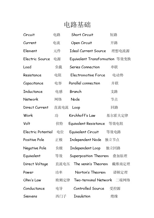
电路基础Circuit 电路Short Circuit 短路Current 电流Open Circuit 开路Element 元件Ideal Current Source 理想电流源Electric Source 电源Equivalent Transformation 等效变换Load 负载Series Connection 串联Resistance 电阻Electromotive Force 电动势Capacitance 电容Parallel connection 并联Inductance 电感Branch 支路Network 网络Node 节点Direct Current 直流电流Loop 回路Work 功Kirchhoff’s Law 基尔霍夫定律Volt 伏特Equivalent Resistance 等效电阻Electric Potential 电位Equivalent Circuit 等效电路Positive Pole 正极Independent Node 独立节点Negative Pole 负极Independent Loop 独立回路Equivalent 等效Superposition Theorem 叠加原理Direct Voltage 直流电压The venin’s Theorem 戴维南定理Power 功率Norton’s Theorem 诺顿定理Ohm’s Law 欧姆定律Two-terminal Network 二端网络Conductance 电导Controlled Source 受控源Siemens 西门子Insulation 绝缘Ideal Voltage Source 理想电压源Magnetic Flux 磁通Magnetic Flux Linkage 磁通链Angular Frequency 角频率Self-Inductance 自感Initial phase 初相位Lenz’s Law 楞次定律Phase Difference 相位差Excitation 激励In Phase 同相Response 响应Effective Value 有效值First-order Circuit 一阶电路Root-mean-square Value均方根值Law of Switching 换路定则Vector 矢量Steady State 稳态Phasor 相量Zero-input Response 零输入响应Complex Number 复数Characteristic Equation 特征方程Model 复数的模Time Constant 时间常数Argument 复数的幅角Zero-state Response 零状态响应Instantaneous Power瞬时功率Complete Response 全响应Active Power 有功功率Steady state Component 稳态分量Inductive Reactance 感抗Transient Component 暂态分量Capacitive Reactance 容抗Alternating Current Circuit 交流电路Lag 滞后Instantaneous value 瞬时值Reactance 电抗Period 周期Complex Impedance 复数阻抗Frequency 频率Impedance Angle 阻抗角Sinusoid 正弦量Impedance Triangle 阻抗三角形Maximum 最大值Inductive Circuit 感性电路Amplitude 幅值Capacitive Circuit 容性电路Phasor Diagram 电压向量图Phase Wire 端线、相线Voltage Triangle 电压三角形Line Voltage 线电压Complex admittance 导纳Phase Voltage 相电压Power Factor 功率因数Line Current 线电流Apparent Power 视在功率Phase Current 相电流Rated value 额定值Reactive Power 无功功率Resonance 谐振Series Resonance 串联谐振Power Triangle 功率三角形Resonance frequency 谐振频率Quality factor 品质因数Parallel Resonance 并联谐振Fourier Series 傅里叶级数Harmonic 谐波Fundamental harmonic 基波Higher Harmonic 高次谐波Three Phase Circuit 三相电路Phase Sequence 相序Star Connection 星形(Y形)接法Delta Connection 三角形(Δ形)接法Three phase four wire system 三相四线制Three phase three wire system 三相三线制模拟电子技术基础Intrinsic Semiconductor 本征半导体Inversion Layer 反型层Hole 空穴Threshold Voltage 开启电压Carrier 载流子Transconductance 跨导Intrinsic Excitation 本征激发Pinch off Voltage 夹断电压Impurity Semiconductor “杂质”半导体Drift Movement 漂移运动Unipolar Transistor单极型晶体管Diffusion Movement 扩散运动Dynamic Load Lines 交流负载线Space-charge Region空间电荷区Nonlinear Distortion非线性失真Reverse Saturation Current 反向饱和电流Avalanche breakdown 雪崩击穿Cutoff Distortion 截止失真Zener breakdown 齐纳击穿Saturation Distortion 饱和失真Barrier Capacitance 势垒电容Emitter Follower 射极跟随器Diffusion Capacitance 扩散电容Bandwidth 通频带Rectifier Circuit 整流电路Frequency Response 频率特性Clipping Circuit 限幅电路Frequency Distortion 频率失真Zener Diodes 齐纳二极管Bodeplot 波特图Voltage Regulators 稳压管Output Power 输出功率Bipolar Transistor 双极型晶体管Efficiency 效率Field Effect Transistor 场效应晶体管(FET)Metal-Oxide-Semiconductor金属-氧化物-半导体场效应管(MOS) Junction Field Effect Transistor 结型场效应管(JFET)Common-Emitter(CE) Amplifier 共射极放大电路Common-Collector Amplifier 共集电极放大电路Common-Base Amplifier 共基极放大电路Amplitude Frequency-Response 幅频特性Phase Frequency-Response 相频特性Output Capacitor Less 双电源互补对称电路;无输出电容电路(OCL电路)Cross Over Distortion 交越失真Darlington Connection 复合管Quasi Complementary Emitter Follower 准互补对称电路Output Transformer Less 无输出变压器电路(OTL电路) Integrated Circuit Power Amplifier 集成功率放大电路Integrated circuit 集成电路(IC) Offset Voltage 失调电压Differential Amplifier差动式放大电路Offset Current失调电流Common-mode Signal 共模输入信号Active Load 有源负载Common-mode Gain共模电压放大倍数Parameter 参数Difference-mode Signal 差模信号Difference-mode Gain 差模电压放大倍数Constant Current Source 恒流源Common-mode Rejection Ratio 共模抑制比Current Mirror Source 镜像电流源Small Value Current Source 微电流源Multiple Current Source 多路电流源Integrated Operational Amplifier 集成运算放大器Non-inverting Input Terminal 同相输入端Inverting Input Terminal 反相输入端Open-Loop 开环Negative Feedback 负反馈Positive Feedback 正反馈Return Difference; Desensitivity 反馈深度With Strong Negative Feedback 深度负反馈Ideal Operational Amplifier 理想运算放大器Virtual Short Circuit 虚假短接Virtual Open Circuit 虚断Virtual Ground 虚地Voltage Follower 电压跟随器Integration Circuit 积分运算电路Differentiator 微分器Self Excited Oscillation 自激震荡Phase Margin 相位裕度Compensation Method 补偿方法Gain Margin 幅度裕度Phase Lead Compensation 超前补偿Integrated Analog Multiplier 集成模拟乘法器Variable Transconductance Multiplier 变跨导式乘法器Four-Quadrant Multiplier 四象限乘法器Low Pass Filter低通滤波器(LPF)High Pass Filter高通滤波器(HPF)Band Pass Filter 带通滤波器(BPF)Band Elimination Filter 带阻滤波器(BEF) Stopband 阻带Cut-off Frequency 截止频率Voltage Comparator 电压比较器Zero-Crossing Comparator 过零比较器Clipping 限幅Sensitivity灵敏度Regenerative Comparator 带有滞回特性的比较器Integrated Voltage Comparator 集成电压比较器Analog-Digital Converter 模数转换器;A/D转换器Frequency –Selective Network 选频网络Amplitude Stability 稳幅Crystal 石英晶体Wien bridge 文式桥振荡电路;RC串并联式正弦波振荡电路Pitzo-Electric Effect 压电效应Voltage-Controlled Oscillator 压控振荡器(VCO)VCXO 晶体压控振荡器LCVCO LC压控振荡器VCM压控多谐振荡器Frequency Modulation (FM) 调频Uninterruptible Power System (UPS) 不停电电源Regulated Power Supply直流稳压电源Regulating Device 调整管Bridge Rectifier 桥式整流Pulse Width Modulation 自激式脉冲调宽式Current Overload Protection 过电流保护。
电力电厂英文词汇

变电站transformer substation/substation输电线路transmission lines用户 consumer制药厂pharmaceutical factory机械制造厂 machine manufactory接线 wiring倒闸操作switch-over operation变压器Transformer主变main transformer升压变step-up transformer降压变step-down transformer升压站booster (feeding) station有载调压变压器: transformer fitted with OLTC(on-load tap-changer)电动机 Motor继电器保护 Relay protection火力发电厂 thermal power plant(fossil- fired power plant)电磁感应原理 Electromagnetic Induction Principle定子线圈(绕组)stator winding磁场magnetic field三相交流电three phase AC开关柜switchgear检修工作票maintenance work permit监盘定位制度system of monitoring operation terminals and fixed positions 巡回检查制度 (itinerant) walking-down and inspection system设备切换制度 equipment switch-over(change-over) system频率(周波)frequency单母分段single bus section双母接线double bus-bar wiring单元接线unit wiring出线电压output voltage中性点neutral point无载调压:No-load tap-changer备用电源stand-by power supply架空线overhead wire厂用电源 auxiliary power source柴油发电机组diesel generator unit一次接线Primary wiring隔离开关(刀闸)disconnector接地刀闸earthing disconnector拆 dismantle控制回路control loop电压互感器PT VT(potential transformer/voltage transformer)电流互感器 CT(current transformer)熔断器fuse手车式(推拉式)开关 drawable circuit breaker送电范围power transmission scope操作票operation permit发令时间Issued time单人操作Single operator operation值班员operator同步电机synchronous motor励磁excitation定子绕组stator winding定子铁芯 stator iron core冷却器cooler转子铁芯rotor iron core转子绕组rotor winding支持瓷瓶support porcelain bottle同步发电机 synchronous generator原动机 engine(prime mover)励磁电流excitation current磁力线magnetic force line电磁感应原理electromagnetic induction principle电动势electricmotive force(EMF)直接耦合direct-coupling封闭循环空气冷却enclosed circulating air cooling无刷励磁brushless excitation同轴无刷励磁机coaxial brushless exciter永磁副励磁机permanent magnetic standby exciter绝缘漆insulated paint自动励磁电压automatic excitation voltage regulator 短路 short-circuit铝压圈aluminum pressed ring不锈钢分块齿压板stainless steel block tooth sole plate穿心螺杆through-core screw rod鼠笼式结构squirrel-cage structure立式支撑结构vertical support structure玻璃纤维glass fiber锥环conical ring定子线棒stator winding rod滑移层slipping layer转轴rotation shaft径向风道冷却 radial air duct cooling封闭循环系统enclosed circulating system功率因数Power factor最大连续输出功率Maximum continuous output power交流励磁机AC exciter可控硅thyristor不可控硅二极管non-thyristor diode交流电枢绕组 AC armature winding硅整流器 silicon rectifier自励self-excited他励 separately excited磁场电流 magnetic field current励磁变压器Excitation transformer整流装置Rectifying equipment启励回路start-up excitation loop过电压保护装置 over-voltage protection device数字式自动电压调节器Digital automatic voltage regulator 导通角conduction angle灭磁开关deexcitation breaker套筒式结构sleeve-type structure同轴结构coaxial structure调整偏差regulating deviation (error)压板sole plate空气冷却系统air-cooling system最大偏差maximum deviation大轴接地电刷the grounding electrical brush of big shaft 绝缘电阻 insulating resistance主汽门main steam stop valve强行励磁forced excitation相位phase相序phase sequence有功负荷active load轴承排油温度oil-discharging temperature of bearing 一次绕组primary winding二次绕组secondary winding交变磁通alternating flux电磁感应electromagnetic induction压降pressure drop阻抗 impedance匝数 turns高压套管High voltage bushing分接开关Tap changer.低压套管Low voltage bushing瓦斯继电器Gas relay防爆管explosion- preventing pipe地脚螺栓 anchor bolt油样活门Oil sampling valve放油阀门Oil-discharge valve油枕Oil conservator储油箱oil storage tank吸湿器moisture absorber散热器heat radiator瓦斯保护gas protection差动保护differential protection放气或放油塞子gas drain or oil drain plug温度计thermometer电抗器reactor放电现象arc discharge phenomenon避雷器 arrester引线 lead渗油oil infiltration硅胶silica gel散热翅radiation fin引线接头lead connector安全气道safety gas duct油位oil level远方电动调整remote motor-driven regulation手动调整 manual regulation二次回路secondary circuit整定值set point录波Oscilloscope微机保护装置microcomputer protection device复位按钮 reset button继保人员relay protection operator跳闸压板 trip sole plate高内阻电压表high inner-resistance voltmeter万用表multimeter校灯 a measurement device with a lamp电压回路断线故障broken-line failure in voltage circuit 总闭锁动作general blockage action正极anode负极cathode极性polarity母差互感器bus-bar differential transformer负极(阴极)cathode阴极反馈电路:cathode feedback circuit母差回路bus bar differential circuit.分布式数据处理系统distributed data processing system 数据采集系统 data acquisition systemI/O接口 I/O interface光纤通道optical fiber channel,监控系统monitoring system集中控制屏centralized control screen人工干预manual intervention越限记录out-of-limit record.上级调度higher-level dispatcher时钟功能clock function五防联锁功能five-guard-against interlock functions 非同期闭锁non-synchronous lockout自投装置self-operating equipment异步电动机asynchronous motor端盖End shield(cover)接线盒junction box绝缘电阻insulation resistance电阻表ohmmeter滑动轴承sliding bearing滚动轴承rolling bearing润滑脂grease铭牌nameplate环境温度ambient temperature备用机组spare unit靠背轮coupling护罩cover glass启动装置start up equipment地测温装置temperature measurement device温度记录仪thermograph滑环短接装置short-circuit equipment of slip ring 整流器rectifier熔芯fuse core大容量低压电动机large-capacity low-voltage motor合闸电压closing voltage隔离手车Isolated drawable circuit breaker电压手车voltage drawable circuit breaker电磁锁electromagnetic lock底盘chassis断路器手车drawable circuit breaker接地闭锁开关grounding lockout switch防误装置error-prevent device真空断路器vacuum breaker绝缘子 insulator闪络现象 arc-discharging phenomenon绝缘拉杆insulated tension rod充电装置charging set直流油泵联动DC oil pump interlock蓄电池battery浮充状态floating charging conditions失磁loss-excitation灌浆grouting空载电压 no-load voltage同轴无刷励磁机coaxial brushless exciter零序电压zero sequence voltage遥测 remote sensing/measuring遥控 remote control/capture远处发信号 remote signaling电抗 reactance实时运行参数 real-time operation parameter非同期(异步) asynchronous定子风槽 stator ventilating slot短路故障开断 short-circuit fault opening电磁操作机构 electromagnetic operating mechanism二次设备 secondary equipment二次插头 secondary plug机械闭锁 mechanical lock/bloc免维护铅酸蓄电池 maintenance-free lead-acid storage battery终止电压 cut-off voltage极性 polarity顶轴油泵 lifting(jacking) oil pump高频模块方案 high frequency skid program负序电流 negative-sequence current冲击电流 impulse current解列 step-out/out-of-step/disconnection/switch off/结露 dew formation干式变压器绕组 dry-type transformer winding充油套管 oil-filled bushing电压比 voltage ratio内阻抗压降 internal impedance voltage drop自然油循环 natural oil circulation磁通势magneto-motive force无功负荷预报曲线 reactive load forecast curve轴瓦bearing liner联跳 interlock trip并接 parallel connection他励旋转硅整流器 separately excited rotating silicon rectifier 径向风道 radial air duct自并励静止励磁系统 self-excited static excitation system 封闭循环系统 enclosed circulating system槽楔 slot wedge轴流风扇 axial(flow) fan电势波形 potential wave通风副槽 sub-slot ventilation嵌线 inserting wires径向嵌线槽 radial wire-inserting slot刚-柔结构 rigid-flexible structure定子线棒stator winding bar轴向滑移层 axial slipping layer绝缘垫块 insulated block适形材料 suitable shape material对地绝缘 grounding insulation铁芯振动 iron core vibration抗磁性 diamagnetism外压 external voltage内压 internal voltage高导磁 high conductivity magnetic相对运动 relative motion护环 retaining ring倒送电 back energization保护回路 protection circuit验电笔 electroscopic pen验电器:eletroscope保安电源 emergency power supply装拆接地线install/disassembly grounding wire备用电源 stand-by/backup power supply降压 voltage drop单相接地保护 single phase earthing protection厂用电电压等级 plant voltage grade变压器高压侧中性点 neutral point at high-voltage side transformer 降压变压器 step-down/reducing transformer发变组单元接线 generator-transformer unit connection单母线带旁路 single bus with bypass升压 voltage raising交接班制 shift handover system出线 outgoing feeder进线incoming feeder启励回路field/excitation start-up circuit铝绞线 aluminum conductor/twist定位棒/间隔棒 spacer rod线夹 clamp拉线 stay拉线杆:Stayed pole回填 backfill等电位作业 equal potential operation带电作业 live operation磁场magnetic field电磁感应Electromagnetic Induction灭弧 arc suppression / extinction扩容器:flash tank/expander位筋:localization rib加强筋reinforce rib排污:blow down共箱母线:non-segregated phase busbar 分相封闭母线segregated bus封闭母线 enclosed bus自同期:self–synchronization准同期:pre-synchronization假同期:wattless synchronization迟相方式:lagging phase mode 进相方式leading phase mode脉冲Pulse节电模式Power Save Mode冗余二极管redundant diode匝数比turns ratio电容器:Capacitor有功损耗:active power loss无功损耗:reactive power loss 空载损耗:no-load loss空载电流:no-load current正序阻抗:positive sequence impedance 负序阻抗:negative sequence impedance 零序阻抗:zero sequence impedance 分段母线 sectional bus双母线 double bus单母线 single bus。
CMOS超大规模集成电路设计经典教材
Source Gate Drain
Polysilicon
SiO2
0
n+
n+
SD
p
bulk Si
0: Introduction
CMOS VLSI Design 4th Ed.
7
nMOS Operation Cont.
When the gate is at a high voltage:
– Positive charge on gate of MOS capacitor
– Negative charge attracted to body
– Inverts a channel under gate to n-type
– Now current can flow through n-type silicon from source through channel to drain, transistor is ON
– Fast, cheap, low power transistors Today: How to build your own simple CMOS chip
– CMOS transistors – Building logic gates from transistors – Transistor layout and fabrication Rest of the course: How to build a good CMOS chip
capacitor
Source Gate Drain
– Even though gate is
no longer made of metal
Polysilicon SiO2
n+
2.4_GHz频段射频前端高线性度SiGe低噪声放大器设计
第50 卷第 10 期2023年10 月Vol.50,No.10Oct. 2023湖南大学学报(自然科学版)Journal of Hunan University(Natural Sciences)2.4 GHz频段射频前端高线性度SiGe低噪声放大器设计傅海鹏†,史昕宇(天津大学微电子学院,天津 300072)摘要:为满足高性能射频前端接收部分对高线性度的需求,基于SiGe BiCMOS工艺设计并实现了一款工作在2.4 GHz频段的高线性度低噪声放大器(Low Noise Amplifier,LNA).该放大器采用Cascode结构在增益与噪声之间取得平衡,在Cascode结构输入和输出间并联反馈电容,实现输入端噪声与增益的同时匹配.设计了一种改进的动态偏置有源电流镜以提升输入1 dB压缩点及输入三阶交调点的线性度指标.为满足应用需求,LNA与射频开关及电源模块集成组成低噪声射频前端接收芯片进行流片加工测试.测试结果表明:在工作频率2.4 ~2.5GHz内,整个接收芯片增益为14.6 ~15.2 dB,S11、S22<-9.8 dB,NF<2.1 dB,2.45 GHz输入1 dB压缩点为-2.7 dBm,输入三阶交调点为+12 dBm.芯片面积为1.23 mm×0.91 mm.该测试结果与仿真结果表现出较好的一致性,所设计的LNA展现出了较好的线性度表现.关键词:低噪声放大器;线性度;射频前端芯片;BiCMOS工艺中图分类号:TN402 文献标志码:ADesign of 2.4 GHz RF Front-end High Linearity SiGe Low Noise AmplifierFU Haipeng†,SHI Xinyu(School of Microelectronics,Tianjin University,Tianjin 300072,China)Abstract:To meet the high linearity requirement of high-performance RF front-end receivers, a high linearity low noise amplifier (LNA)operating at 2.4 GHz based on SiGe BiCMOS technology is proposed. The amplifier adopts the cascade structure to achieve a balance between gain and noise, and the feedback capacitor is connected in parallel between the input and output of the Cascode structure to achieve simultaneous noise and power match. An improved dynamic bias active current mirror is designed to improve the linearity parameters of the input 1 dB compression point and the input-referred third-order intercept point. To meet the requirements in application, LNA is integrated with an RF switch and power module to form an RF receiver front-end chip for processing and testing. The test results show that: within the operating frequency range of 2.4 ~ 2.5 GHz, the gain of the whole receiver chip is 14.6 ~ 15.2 dB. Return loss < -9.8 dB, and NF < 2.1 dB. At 2.45 GHz, the input 1 dB compression point is -2.7 dBm, and the input-referred third-order intercept point is +12 dBm. The chip area is 1.23 mm×0.91 mm. The test results are consistent with the simulation results, and the designed LNA exhibits good linearity performance.∗收稿日期:2023-02-22基金项目:国家自然科学基金资助项目(62074110),National Natural Science Foundation of China(62074110)作者简介:傅海鹏(1985—),男,黑龙江齐齐哈尔人,天津大学副教授† 通信联系人,E-mail:************.cn文章编号:1674-2974(2023)10-0077-07DOI:10.16339/ki.hdxbzkb.2023240湖南大学学报(自然科学版)2023 年Key words:low noise amplifiers;linearity;radio frequency front-end chip;BiCMOS technology低噪声放大器要求在自身不引入较大噪声的同时,将接收到的微弱信号进行线性放大.作为接收机中的第一个放大器,LNA的性能在很大程度上影响整个系统的噪声、线性度、灵敏度等指标.近年来,通信技术的发展和进步让视频会议、网络教学等各种应用场景得以实现,改变了人们的生活方式[1-3].为了适应不断扩大的接入设备数量,满足不断增长的数据吞吐量及速率需求,无线通信协议标准也在不断发展.其中,无线通信协议中诸如调制阶数的提升及系统灵敏度要求的提高对射频前端接收部分的线性度提出了更高的需求.这为LNA的设计带来了新的挑战,LNA需要具有更高的线性度、更低噪声、更高增益,以及更低的面积成本等[4].为实现高线性度需求,文献[5]采用多栅晶体管(Multiple Gated Transistor,MGTR)结构,分别将主、从CMOS晶体管偏置在饱和区和亚阈值区,实现对整体跨导二次导数的抵消,从而提升线性度.然而,该方案仅适用于CMOS工艺.文献[6]采用堆叠晶体管的方法设计了一种堆叠三级的cascode低噪声放大器.堆叠使得放大器可以使用更高的电源电压,从而获得更大的信号摆幅范围.功耗的提升也使得线性度得以提升.但这显著牺牲了功耗,不符合低功耗应用的发展趋势.文献[7]通过改进偏置电路提升线性度,但是其在大信号时,经电阻泄漏的射频电流会直接流入偏置电路中,偏置电路与放大器间镇流电阻的压降变化仍会带来低噪声放大器输入1 dB压缩点的前移,恶化放大器线性度.从工艺考虑,虽然CMOS工艺具有成本较低、易于集成等优势,但是噪声和线性度较差[8].而GaAs等Ⅲ/Ⅴ族工艺与之相反,性能优秀,但价格高昂且不易集成[9].与上述主流工艺对比,SiGe BiCMOS工艺不仅具有CMOS工艺易于集成的特点,还具有可与GaAs等Ⅲ/Ⅴ族工艺相比拟的性能和价格优势,是一种适合射频LNA设计的具有高性价比的折中选择[10].针对上述挑战并考虑工艺特点,本文采用SiGe BiCMOS工艺,设计并实现了一款工作在2.4 GHz频段的射频前端LNA.通过并联电容反馈技术在输入端同时实现增益和噪声匹配,并结合SiGe工艺特点,采用改进的动态偏置电路,克服镇流电阻压降影响,对泄漏的射频电流也加以利用,在不提升静态功耗的同时,实现线性度提升.为适应不同强度信号下的工作情况,该LNA可在LNA模式和旁路(Bypass)模式间切换.1 电路设计本文提出的全集成LNA整体框图如图1所示.整体电路由LNA、偏置电路、单刀双掷(Single PoleDouble Throw,SPDT)收发开关及Bypass支路构成.芯片整体通过单刀双掷开关选通发射、接收支路. LNA接收部分在输入信号较小时,通过逻辑控制开关使电路工作在LNA模式,实现低噪声放大功能.在输入信号较大时,电路工作在Bypass模式,对信号进行旁路衰减,供后级电路处理.1.1 开关设计本文使用的单刀双掷开关如图2所示.开关电路结构采用串并联结构,导通时开启串联支路,关闭并联支路,实现导通低插入损耗;关断时关闭串联支路,导通并联支路,实现关断高隔离度.由于发射、接收支路具有不同的功率容量需求,整体电路设计为非对称结构.当LNA_EN为高电平,PA_EN为低电平时,射频开关选通接收支路,M1管关断隔离发射支路,天线ANT端口接收信号经过M2、M3管从RX端输出至LNA主体放大;当LNA_EN为低电平,PA_EN为高电平时,M2、M3关断隔离接收支路,PA发出的大功率信号由TX端口经过M1管从ANT端输出.1.2 LNA及Bypass设计低噪声放大器在稳定的条件下,主要性能指标图1 全集成LNA框图Fig.1 Block diagram of fully integrated LNA78第 10 期傅海鹏等:2.4 GHz 频段射频前端高线性度SiGe 低噪声放大器设计包含噪声系数、增益及线性度,良好的设计需要在三者之间权衡折中,一般噪声系数和增益的优先级较高[11-12].本文所设计的LNA 放大器部分如图3所示,放大器主体由三极管Q CE 和Q CB 构成器件数较少的共射共基结构,减少晶体管噪声贡献并提高放大器增益.采用高Q 值的金丝键合线电感L S 组成发射极电感反馈结构保持放大器良好的稳定性,并参与输入阻抗实部匹配.考虑三极管在电流密度一定的条件下,其最小噪声系数将独立于晶体管大小.并且,共射共基极放大器的线性度与集电极工作电流I C 正相关.因此,在功耗范围内采用大尺寸、低电流密度的三极管实现噪声与线性度的折中设计.尽管这将导致输入阻抗的实部低于50 Ω,使输入匹配复杂化,但采用额外的并联电容反馈C F 和L 1、C 1构成的L 型匹配网络仍可以实现输入端噪声与增益的同时匹配.具体如图4所示,Z S 为50 Ω射频端口阻抗经过射频开关接收支路后在RX 端口体现的阻抗值.将L 1、C 1构成的L 型匹配网络输入阻抗设计为射频开关输出阻抗Z S 的共轭以实现最佳输入匹配,输出阻抗设计为共射共基放大器的最优信号源阻抗实现噪声匹配.并联反馈电容C F 将由负载电感L D 与电容C 3、C 4、C 5构成的T 型匹配网络共同组成的输出负载阻抗Z L 引入输入端匹配,因此可以通过调整C F 、Z L 来使看向晶体管的输入阻抗Z T 等于最佳噪源阻抗的共轭来实现增益匹配.由于引入的Z L 不在输入端,不会对先前噪声匹配产生明显影响,至此,也就实现了晶体管输入阻抗不为50 Ω时的输入端噪声与增益的同时匹配.且反馈电容C F 的引入使得反馈增强,稳定性提高,可以减小对L S 尺寸的需求,进一步优化噪声.结合图3、图4,可以推导出具体的输入阻抗为:Z IN =1sC 1//(sL 1+Z T )(1)Z T =Z 1s ()Z L +1sC FZ L ωT +s ()Z L +1sC F(2)Z 1=r BB +L S g m C BE +sL S +1sC BE(3)ωT =g m C BE(4)其中,C 1、L 1分别为L 型输入匹配的电容、电感,Z L 为负载电感L D 与电容C 3、C 4、C 5构成的T 型匹配网络共同组成的输出负载阻抗,C F 为并联反馈电容,r BB 为三极管小信号模型中的基极电阻,L S 为发射极反馈电感,g m 为三极管跨导,C BE 为三极管基极与发射极间寄生电容.当接收机接近信号源时,会接收到较大功率的信号,此时需要Bypass 功能对大功率信号进行旁路,避免信号超出接收电路动态范围,保护低噪声放大器不被损坏.当工作在Bypass 模式时,开关S 1、S 2、S 3、图2 单刀双掷开关原理图Fig.2 Schematic of single pole double throw switch图3 低噪声放大器原理图Fig.3 Schematic of the proposed dual-mode low noise amplifier图4 输入匹配原理图Fig.4 Schematic of the input matching network79湖南大学学报(自然科学版)2023 年S4断开,切断LNA通路.开关S5、S6打开,借由S5、S6开关的导通电阻与电阻R2和电容C7所在的支路一同构成T型衰减结构,并可以通过电容C6、C8分别调节Bypass模式下的输入、输出匹配特性,通过电容C7调整带内衰减平坦度,实现Bypass模式的信号衰减功能.1.3 线性度提升偏置电路设计偏置电路为晶体管提供合适的静态工作点.传统的有源偏置电路常采用电流镜结构,如图5所示.晶体管集电极电流I C与基极-发射极之间电压V BE的关系可写为:I C=I S exp(V BE V T)(5)式中:V T为热电压;I S为饱和电流.上式得出,当图5中晶体管Q2与Q3具有相同V BE 时,电流镜左右两边必然流过相同的电流.这就是电流镜的工作原理.假设LNA共射管Q CE叠加射频信号后,式(5)可改写为如式(6)所示,其中V RF为输入射频信号幅度.经过泰勒展开后可得式(7).I C=I S expéëêêV BE+V RF·sin ()2πft V Tùûúú(6)I C≈I S exp (V BE V T)éëêê54+sin (2πft)-cos ()4πft4ùûúúV RF V T(7)由上式可以得出,射频信号的输入会给集电极电流I C引入额外的直流分量,且随着输入射频信号增大,I C的直流部分将迅速升高.这意味着,随着输入射频信号增大,升高的I C将使得基极电流几乎同步升高,在镇流电阻上产生更大的压降,迫使共射管Q CE直流偏置电压降低,晶体管跨导下降,进而带来放大器增益的下降,使得放大器的1 dB压缩点提前到来,影响LNA线性度表现.因此,为提高LNA的线性度,本文采用如图6所示的动态偏置电路对LNA进行偏置.I Bias采用基准模块产生的恒定电流.将原本的镇流电阻R拆分为电阻R2、R3,则Q CE基极电流增大在R3上产生的额外压降仅会使得Q2各极电位同步抬升,避免了上述传统结构中镇流电阻对LNA线性度的影响.当LNA工作在小信号情况时,该偏置电路为放大器晶体管提供稳定偏置.而当输入射频信号增大,使得LNA共射管Q CE基极电压出现下降时,Q1基极电压将随之降低.同时,泄露的射频电流经C1流入R1,抬升Q1发射极电压,使得Q1集电极电流减小.此时,I Bias中将有更多电流成为Q2的基极电流,并经过Q2的电流放大作用,产生更多电流流入Q CE基极.最终,额外电流的注入将提高Q CE偏置电压,延缓Q CE跨导下降导致的放大器增益下降,实现动态偏置效果,提高LNA线性度.仿真得到在使用上述两种偏置电路时,Q CE晶体管基极-发射极电压V BE随输入功率变化的关系如图7所示.从图7可对比得出,使用传统电流镜偏置的晶体管V BE在输入功率高于-10 dBm后出现快速下降,并在输入功率达到+5 dBm时,已下降约200 mV.而同等条件下,采用动态偏置电路结构进行偏置的晶体管V BE仅下降10 mV.以上结果表明,动态偏置电图5 传统电流镜有源偏置电路原理图Fig.5 Schematic of traditional active bias circuit usingcurrent mirror图6 动态偏置电路原理图Fig.6 Schematic of dynamic bias circuit 80第 10 期傅海鹏等:2.4 GHz 频段射频前端高线性度SiGe 低噪声放大器设计路可以更好地稳定放大器的静态工作点,减弱输入功率升高时,晶体管跨导变化导致的增益下降,改善电路的线性度.2 仿真及测试结果对比分析本节介绍芯片的仿真与测试结果.芯片的显微镜照片如图8所示.芯片面积为1.23 mm×0.91 mm.测试时,芯片的所有pad 均由金丝键合线连接至片外测试板.测试板照片如图9所示.测试板使用4350板材.S 参数的仿真与测试结果对比如图10所示.仿真结果表明,在2.4 ~2.5 GHz 内,LNA 的S 21为15.1~15.5 dB ,S 11<-20 dB ,S 22<-13.8 dB.测试结果表明,在相应频带内,S 21为14.6 ~15.2 dB ,S 11<-18 dB ,S 22<-9.8 dB. S 参数的测试结果与仿真结果一致性较高.噪声系数的仿真与测试结果对比如图11所示.在2.4 ~2.5 GHz 内,仿真噪声系数<1.85 dB ,实测噪声系数在1.9~2.06 dB 内.噪声系数的仿真与实测结果相差接近0.2 dB ,主要为测试板射频走线及接头损耗所致,可以认为仿真与测试结果一致.图12及图13展示了LNA 线性度测试结果.测试结果表明,该LNA 在中心频点2.45 GHz 处输入1 dB图7 电路使用传统电流镜偏置与动态偏置的V BE 随输入功率变化Fig.7 V BE versus input power for circuit using conventionalcurrent mirror bias and dynamic bias图8 芯片显微镜照片Fig.8 Microscope photo of the chip图9 测试板照片Fig.9 Photo of the test board图10 S 参数仿真与测试结果Fig.10 Simulation and test results of S-parameters图11 噪声系数仿真与测试结果Fig.11 Simulation and test results of noise figure81湖南大学学报(自然科学版)2023 年压缩点接近-2.7 dBm ,其输入三阶交调点超过+12 dBm. LNA 实现了较优的线性度表现.表1展示了本设计与近年其他低噪声放大器的性能比较结果.从对比结果可以看出,本文所设计的低噪声放大器各项性能指标较为均衡,增益较高,噪声系数相对较小,且本设计的输入三阶交调点指标较为突出,该低噪声放大器具有较为优秀的线性度水平.3 结 论本文提出了一款基于SiGe 工艺的高线性度低噪声放大器.设计采用电容反馈结构和L 型输入匹配实现放大器增益与噪声的同时匹配优化,并采用改进的动态偏置电路提升LNA 的线性度表现.实测结果表明,在2.4 ~2.5 GHz 的工作频带内,电路增益为14.6 ~15.2 dB ,噪声系数在2.1 dB 以内,输入输出匹配良好,且整体仿真结果与加工实测结果表现出较好的一致性.线性度测试结果表明该LNA 在中心频点2.45 GHz 处输入1 dB 压缩点接近-2.7 dBm ,电路输入三阶交调点达到了+12 dBm ,所设计的低噪声放大器具有较高的线性度.参考文献[1]胡锦,翟媛,郝明丽,等.应用于WLAN 的SiGe 射频功率放大器的设计[J ].湖南大学学报(自然科学版),2012,39(10):56-59.HU J ,ZHAI Y ,HAO M L ,et al .Design of SiGe RF poweramplifier for WLAN [J ].Journal of Hunan University (NaturalSciences ),2012,39(10):56-59.(in Chinese )[2]LI C J ,WANG X X ,JAIN V ,et al .2.4/5.5GHz LNA switchdesigns based on high resistive substrate 0.35um SiGe BiCMOS [C ]//2015 IEEE 11th International Conference on ASIC (ASICON ). Chengdu :IEEE ,2016:1-4.[3]刘祖华,刘斌,黄亮,等.应用于WLAN 的低噪声放大器及射频前端的设计[J ].电子技术应用,2014,40(1):38-40.LIU Z H ,LIU B ,HUANG L ,et al .Design of low noise amplifier and RF front-end for WLAN [J ].Application of ElectronicTechnique ,2014,40(1):38-40.(in Chinese )[4]KANG B ,YU J ,SHIN H ,et al .Design and analysis of a cascodebipolar low-noise amplifier with capacitive shunt feedback under power-constraint [J ].IEEE Transactions on Microwave Theoryand Techniques ,2011,59(6):1539-1551.[5]KIM T W ,KIM B ,LEE K .Highly linear receiver front-endadopting MOSFET transconductance linearization by multiple gated transistors [J ].IEEE Journal of Solid-State Circuits ,2004,39(1):223-229.[6]DAVULCU M ,ÇALıŞKAN C ,KALYONCU İ,et al .An X-bandSiGe BiCMOS triple-cascode LNA with boosted gain and P1dB [J ].IEEE Transactions on Circuits and Systems II :Express Briefs ,2018,65(8):994-998.[7]LUO Y B ,SHI J A ,MA C Y ,et al .A high linearity SiGeHBT图12 输入1 dB 压缩点测试结果Fig.12 Test results of input 1 dB compression point图13 输入三阶交调点测试结果Fig.13 Test results of input-referred third-order intercept point表1 低噪声放大器性能总结Tab.1 Summary of the low noise amplifier performance文献文献[13]文献[14]文献[15]本文工艺CMOS SiGe SOISiGe 增益/dB 11.213.51514.6 ~15.2噪声系数/dB3.92.81.82.06输入1 dB 压缩点/dBm――-8.5-2.7输入三阶交调点/dBm3.9-1.53.51282第 10 期傅海鹏等:2.4 GHz频段射频前端高线性度SiGe低噪声放大器设计LNA for GPS receiver[J].Journal of Semiconductors,2014,35(4):045001.[8]ZHANG H,SÁNCHEZ-SINENCIO E.Linearization techniques for CMOS low noise amplifiers:a tutorial[J].IEEE Transactionson Circuits and Systems I:Regular Papers,2011,58(1):22-36.[9]饶忠君,张志浩,章国豪.2.3~2.7 GHz双模式低噪声射频接收前端全集成芯片的设计[J].电子技术应用,2021,47(7):17-20.RAO Z J,ZHANG Z H,ZHANG G H.Design of a 2.3~2.7 GHzdual-mode low-noise RF receiver front end[J].Application ofElectronic Technique,2021,47(7):17-20.(in Chinese)[10]井凯.SiGe HBT低噪声放大器的研究[D].西安:西安电子科技大学,2016.JING K.Research on SiGe HBT low noise amplifier[D].Xi’an:Xidian University,2016.(in Chinese)[11]NGUYEN T K,KIM C H,IHM G J,et al.CMOS low-noise amplifier design optimization techniques[J].IEEE Transactionson Microwave Theory and Techniques,2004,52(5):1433-1442.[12]曾健平,樊明,陈铖颖,等.应用于眼压信号检测的低噪声前置放大器设计[J].湖南大学学报(自然科学版),2017,44(8):112-116.ZENG J P,FAN M,CHEN C Y,et al.Design of low-noisepreamplifier for application of intraocular pressure signal-detection[J].Journal of Hunan University (Natural Sciences),2017,44(8):112-116.(in Chinese)[13]陈福栈,甘业兵,罗彦彬,等.一种2.4 GHz多模块集成CMOS 射频前端芯片[J].微电子学与计算机,2020,37(12):27-32.CHEN F Z,GAN Y B,LUO Y B,et al.A 2.4 GHz multi-moduleCMOS RF front-end chip[J].Microelectronics & Computer,2020,37(12):27-32.(in Chinese)[14]刘启,甘业兵,黄武康.一种2.4 GHz SiGe全集成射频前端电路[J].微电子学与计算机,2020,37(10):7-12.LIU Q,GAN Y B,HUANG W K.A 2.4 GHz SiGe full integratedRF front-end[J].Microelectronics & Computer,2020,37(10):7-12.(in Chinese)[15]PARAT D,SERHAN A,REYNIER P,et al.A linear high-power reconfigurable SOI-CMOS front-end module for WI-FI 6/6Eapplications[C]//2022 IEEE Radio Frequency Integrated CircuitsSymposium (RFIC). Denver,CO:IEEE,2022:39-42.83。
反激有源钳位(Active-Clamp Flyback)
3. ACTIVE-CLAMP FLYBACK AS AN ISOLATED PFC FRONT-END CONVERTER
46
peak current stress and RMS currents than CCM operation. However, ZVS can still be realized with unidirectional magnetizing current by utilizing the energy stored in the resonant inductor [44]. The presence of the resonant inductor also helps to softly commute the turn-off of the output rectifier, resulting in reduced output noise and rectifier switching losses. This would also be a particular advantage in high output voltage applications where slower rectifiers are more likely to be used. This chapter presents evaluation of a constant-frequency, soft switching, active-clamp flyback converter suitable for both PFC and DC/DC conversion applications. The basic principle of operation is analyzed and a design procedure is developed. Experimental results are then presented which illustrate converter function and verify the analysis presented. These results are then extended to active-clamp flyback single-stage and interleaved PFC applications where the system power levels are limited to about 500 600 W.
- 1、下载文档前请自行甄别文档内容的完整性,平台不提供额外的编辑、内容补充、找答案等附加服务。
- 2、"仅部分预览"的文档,不可在线预览部分如存在完整性等问题,可反馈申请退款(可完整预览的文档不适用该条件!)。
- 3、如文档侵犯您的权益,请联系客服反馈,我们会尽快为您处理(人工客服工作时间:9:00-18:30)。
A Capacitor-Less CMOS Active FeedbackLow-Dropout Regulator With Slew-Rate Enhancement for Portable On-Chip Application Edward N.Y.Ho and Philip K.T.Mok,Senior Member,IEEEAbstract—A low-dropout regulator for on-chip application with active feedback and a slew-rate enhancement circuit to minimize compensation capacitance and speed up transient response is presented in this brief.The idea has been modeled and exper-imentally verified in a standard0.35-μm CMOS process.The total compensation capacitance is7pF.From experimental results, the implemented regulator can operate from a supply voltage of 1.8–4.5V with a minimum dropout voltage of0.2V at a maximum 100-mA load and I Q of20μA.Index Terms—Active feedback,analog circuits,capacitor-less low dropout(LDO),dc–dc regulator,low-dropout(LDO)voltage regulators.I.I NTRODUCTIONL OW-DROPOUT(LDO)regulators are widely used in inte-grated on-chip power management applications in mobile and battery-powered devices requiring clean supply voltage and small device area[1],[2].Minimizing quiescent current and dropout voltage while maintaining good regulation and fast response is the main issue of the LDO regulator design. For portable applications,off-chip components such as output filtering capacitors should be minimized to reduce printed-circuit-board layout space and speed up manufacturing process. However,to provide good performance,current LDO regula-tors usually require off-chipfiltering capacitors ranging from 1to10μF[3]–[7]for a stable output voltage.For on-chip application,this amount of capacitance cannot be integrated in silicon.An output capacitor-less LDO regulator is needed for this application.During load transients,the output capacitor acts as a charge buffer to absorb(provide)the current difference between the load and the power transistor.Reduction of the outputfiltering capacitor will lead to severe output voltage changes during fast load current transients,which the power-line-sensitive devices supplied by the LDO regulator cannot tolerate.Since the output capacitor is small,a dominant pole will no longer be located at the output node,unlike the typical LDO regulators.Manuscript received July16,2009;revised October5,2009.First published January22,2010;current version published February26,2010.This work was supported in part by the Research Grant Council of Hong Kong SAR Government,China,under Project617707.This paper was recommended by Associate Editor G.A.Rincon-Mora.The authors are with the Department of Electronic and Computer Engi-neering,The Hong Kong University of Science and Technology,Kowloon, Hong Kong(e-mail:eemok@t.hk).Color versions of one or more of thefigures in this paper are available online at .Digital Object Identifier10.1109/TCSII.2009.2038630Recently,a lot of researchers have proposed various strate-gies to produce output capacitor-less LDO regulators[10]–[12].Many of them are based on pole-splitting compensation approach[10],[12].They view the power MOSFET in an LDO regulator as an amplifier,and,therefore,LDO regulators are variations of two-or three-stage amplifiers.The differences are that an LDO regulator has a large gate capacitor and gain variation at the power MOSFET at different load current condi-tions.This creates problems with stability over different loading current levels and causes serious overshoots/undershoots during fast load transients.To solve these problems,two approaches are proposed:1)Active feedback compensation strategy is used[8]to provide higher loop response and smaller total on-chip compensation capacitors,and2)slew rate enhancement circuitry is implemented to provide an ultrafast feedback re-sponse loop to cater for output variations during output transient dynamics.In this brief,a low quiescent current small on-chip capaci-tance fast load-transient response capacitor-less LDO regulator is presented.The concept of the proposed LDO regulator is discussed in Section II.Circuit implementation and experimen-tal results are given in Sections III and IV,respectively.The conclusion is given in Section V.II.P ROPOSED LDO R EGULATOR S TRUCTUREFig.1(a)displays a conventional three-stage pole-splitting LDO regulator structure.It consists of one two-stage error am-plifier,a pole-splitting network,and a power transistor,which can be treated as an output gain stage to the whole feedback network.To drain large output current,the power transistor has to be large compared with the internal transistors.Therefore, the capacitance at the gate of the power transistor is very large.For on-chip power management purposes,the power line capacitance will be small and in the range of tens to hundreds of picofarads.The response time of the LDO regulator will be slew-rate-limited at the gate of the power transistor.Fig.1(b)illustrates the proposed LDO regulator design with fast transient response.A high-speed loop that consists of G ma and G mx has been introduced into the system to provide extra current to charge and discharge the gate capacitor. Therefore,response time can be much quicker.There are several requirements for the high-speed loop:low power,easy implementation,and small in area.The accuracy of the loop is not a major concern because the loop is used to provide temporary voltage regulation during transient moments.The steady line and load regulation performance is determined by the main high-gain loop.1549-7747/$26.00©2010IEEE2[9].III.C IRCUIT I MPLEMENTATIONHere,the small signal stability of the proposed LDO regula-tor and transient optimized implementation are considered. A.Small Signal AnalysisThe open-loop small signal model of the proposed LDO regulator is shown in Fig.2.It consists mainly of seven blocks:a first-stage amplifier,a second-stage amplifier,an output power transistor,an active feedback block,a slew-rate enhancement block,a feedforward block,and a dynamic feedforward block. The dc gain of the LDO regulator is given by the product of the gain of thefirst-stage amplifier,the second-stage amplifier, and the power transistor.The active feedback compensation capacitor C a forms the dominant pole of the whole system. The active feedback block is effectively operating similar to a signal multiplier to magnify the signal passing through C a to a larger signal[3].This will effectively enable the reduction of the capacitor value of C a.The slew-rate enhancement blockis g m21+1g mp r Ls+C a C1g ma g m21+1g mp r Ls2.(2)A V(s)=V oV in≈A dc(1+sC a r a)1+sp−3db1+C1g m2+C1g m2g mp r L+C a(g mf−g m2)g m2g mps+C a C1g ma g m2+C a C1g ma g m2g mp r L+C1C Lg m2g mps2(1)The corresponding nondominant pole and Q factors are|p H2,3|=g ma g m2g mp r LC a C 1(1+g mp r L )(3)Q H =C a g m2g mp r Lg ma C 1(1+g mp r L ).(4)2)Medium-load condition (around 100μA–10mA).The transconductance of the power transistor de-creases,and the structure starts to work as a three-stage amplifier with large g mp .Therefore,g mp is assumed to be large compared with g m1and g m2,while g mp r L increases to a large value.The denominator of the transfer function is approximately reduced to(1+sC a g m2g mp r o1r o2r L ) 1+C 1g m2s +C 1g m2 C a g ma +C L g mps2(5)with|p M2,3|=g ma g m2g mp1a mp L ma (6)Q M =g m2(g mp C a +C L g ma )g ma g mp C 1.(7)3)Light-load condition (below 100μA).The power transistor drain current decreases,and,eventually,the power transistor operates in the cutoff region.g mp is assumed to be small,while g mp r L becomes very large.In this case,the denominator of the transfer function can be simplified to (1+sC a g m2g mp r o1r o2r L )× 1+s C a (g mf −g m2)g m2g mp +C 1g m2 +s2C 1C Lg m2g mp(8)with|p L2,3|=g m2g mpC 1C L (9)Q L =C 1C L g m2g mpC a (g mf −g m2)+C 1g mp.(10)From the above three cases,it can be observed that thestability of medium and light loads is the most difficult to achieve because of the large overall gain of the LDO regulator and the closer proximity to the unity gain frequency of the second pole.Observing the complex pole and quality factor expression in medium-load and light–load conditions (6),(7),(9),and (10),we may conclude that,in general,we can increase g ma ,g mf ,and C a to stabilize the LDO regulator,that is,by setting the complex pole to twice the gain bandwidth with quality factor equal to 1/√2[9].In the medium-load condition,it givesC a =√2g m1C 1g m2.(11)In light load,the value of C a is given byC a =2C 1C L g m2g mp −C 1g mp(g mf −g m2).(12)Fig.3.(a)Open-loop response of the proposed LDO at V DD =1.8V and V OUT =1.6V.(b)Zoomed-in view of the open-loop response.Together with the stability condition of light load ofg mf >g m2and2C 1C L g m2g mp >C 1g mp (13)the values of C m ,C a ,g ma ,and g mf can be found.In heavy-load and medium-load conditions,both C a and g ma may be used to achieve stability with high UGF.C a can be used to locate the dominant pole location with increments of g ma to decrease the complex pole peaking.In the light-load range,g ma is no longer effective in decreasing the complex pole peaking.g mf should be increased to suppress the Q value at the expenses of extra quiescent current draining from the power transistor to the ground.The location of the left-half-plane zero is required to be set outside the UGF in order not to influence the stability of the proposed design.To fulfill the stability condition in light load,(13)has to be satisfied.The zero will be effectively located at four times of the UGF.The extra phase improvement by the zero is [8]tan −1 g m 1g ma =tan −1 14 =14◦.(14)An open-loop-gain simulation has been performed to studythe stability of the proposed LDO regulator.The simulation is based on a 0.35-μm CMOS model from Austria Mikro System Group (AMS).The power line is modeled as a resistor in parallel with a capacitor of 100pF.C a and C m are chosen to be 1and 6pF,respectively.To guarantee stability for loading current down to zero,g mf has been set to be three times of g m2.The g mf current also sets the minimum current passing through the power transistor and its minimum g mp .From the simulation results in Fig.3,the proposed LDO regulator is stable for loadthe output transient,M17will be turned on,and the slew-rate enhancement circuit will be activated when the undershoot appears.The resulting extra path consisting of g mx can pro-vide extra current for discharging the large gate capacitor of M POWER.As stated during the open-loop analysis section,the slew-rate enhancement block is normally inactive during steady states and only provides current in the transient situation.This will keep the drain current of M17to M19low during the steady-state operation.To ensure stability after the output current transient,the maximum transconductance formed by M17to M19must be set smaller than g m2.In the design,it is achieved by restricting the maximum drain current of M19to be smaller than M12by reducing the size of M19.To ensure that M17is not turned on during the steady state, V B4has to be carefully chosen to be high enough so that V SG of M17is normally less than the threshold voltage of M17.The realization of V B4is shown in Fig.4.By assuming|V TP|= V TN=V T and neglecting the body effectV B4=V DD−V SG(MB2)−V GS(MB3)−V SG(MB4).(15) The gate voltage of M17will beV B4+V SG(M14)+V DSSAT(M16).(16)Therefore,V SG(MB2)+V GS(MB3)+V SG(MB4)−V SG(M14)−V DSSAT(M16)has to be smaller than V T.To achieve this,I B2 needs to be set smaller than I B1,and M B2to M B4have to be biased at the subthreshold region.In the proposed de-sign,V G(M17)is set only400mV below V DD(with V TP∼−700mV)to counter for process variation.IV.E XPERIMENTAL R ESULTSThe proposed LDO regulator has been fabricated with AMS2P4M0.35-μm CMOS technology.The die photo is shownTABLE IP ERFORMANCE S UMMARYFig.6.Measured load transient with a100-pF output capacitor.(a)V DD= 1.8V,V O=1.6V.(b)V DD=3.3V,V O=3.1V.(c)V DD=1.8V, V O=1.6V.(d)V DD=3.3V,V O=3.1V.(e)V DD=1.8V,V O=1.6V.(f)V DD=3.3V,V O=3.1V.(g)V DD=1.8V,V O=1.6V.(h)V DD=3.3V,V O=3.1V.TABLE IIC OMPARISON OF R ESULT。