ROHM无线供电控制IC“BD57020MWV”的参考设计获无线供电WPC Qi认证
英飞凌 FP50R12N2T7P EconoPIM 2 模块 数据表
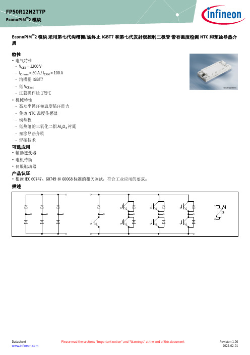
EconoPIM ™2 模块 采用第七代沟槽栅/场终止IGBT7和第七代发射极控制二极管 带有温度检测NTC 和预涂导热介质特性•电气特性-V CES = 1200 V-I C nom = 50 A / I CRM = 100 A -沟槽栅IGBT7-低 V CEsat-过载操作达175°C•机械特性-高功率循环和温度循环能力-集成NTC 温度传感器-铜基板-低热阻的三氧化二铝 Al 2O 3 衬底-预涂导热介质-焊接技术可选应用•辅助逆变器•电机传动•伺服驱动器产品认证•根据 IEC 60747、60749 和 60068标准的相关测试,符合工业应用的要求。
描述FP50R12N2T7PEconoPIM ™2 模块内容描述 . . . . . . . . . . . . . . . . . . . . . . . . . . . . . . . . . . . . . . . . . . . . . . . . . . . . . . . . . . . . . . . . . . . . . . . . . . . . . . . . . . . . . . . . .1特性 . . . . . . . . . . . . . . . . . . . . . . . . . . . . . . . . . . . . . . . . . . . . . . . . . . . . . . . . . . . . . . . . . . . . . . . . . . . . . . . . . . . . . . . . .1可选应用 . . . . . . . . . . . . . . . . . . . . . . . . . . . . . . . . . . . . . . . . . . . . . . . . . . . . . . . . . . . . . . . . . . . . . . . . . . . . . . . . . . . .1产品认证 . . . . . . . . . . . . . . . . . . . . . . . . . . . . . . . . . . . . . . . . . . . . . . . . . . . . . . . . . . . . . . . . . . . . . . . . . . . . . . . . . . . .1内容 . . . . . . . . . . . . . . . . . . . . . . . . . . . . . . . . . . . . . . . . . . . . . . . . . . . . . . . . . . . . . . . . . . . . . . . . . . . . . . . . . . . . . . . . .2 1封装 . . . . . . . . . . . . . . . . . . . . . . . . . . . . . . . . . . . . . . . . . . . . . . . . . . . . . . . . . . . . . . . . . . . . . . . . . . . . . . . . . . . . . . . . .3 2IGBT, 逆变器 . . . . . . . . . . . . . . . . . . . . . . . . . . . . . . . . . . . . . . . . . . . . . . . . . . . . . . . . . . . . . . . . . . . . . . . . . . . . . . . . .3 3二极管,逆变器 . . . . . . . . . . . . . . . . . . . . . . . . . . . . . . . . . . . . . . . . . . . . . . . . . . . . . . . . . . . . . . . . . . . . . . . . . . . . . . .5 4二极管,整流器 . . . . . . . . . . . . . . . . . . . . . . . . . . . . . . . . . . . . . . . . . . . . . . . . . . . . . . . . . . . . . . . . . . . . . . . . . . . . . . .6 5IGBT, 斩波器 . . . . . . . . . . . . . . . . . . . . . . . . . . . . . . . . . . . . . . . . . . . . . . . . . . . . . . . . . . . . . . . . . . . . . . . . . . . . . . . . .7 6Diode-斩波器 . . . . . . . . . . . . . . . . . . . . . . . . . . . . . . . . . . . . . . . . . . . . . . . . . . . . . . . . . . . . . . . . . . . . . . . . . . . . . . . .8 7负温度系数热敏电阻 . . . . . . . . . . . . . . . . . . . . . . . . . . . . . . . . . . . . . . . . . . . . . . . . . . . . . . . . . . . . . . . . . . . . . . . . .9 8特征参数图表 . . . . . . . . . . . . . . . . . . . . . . . . . . . . . . . . . . . . . . . . . . . . . . . . . . . . . . . . . . . . . . . . . . . . . . . . . . . . . . .10 9电路拓扑图 . . . . . . . . . . . . . . . . . . . . . . . . . . . . . . . . . . . . . . . . . . . . . . . . . . . . . . . . . . . . . . . . . . . . . . . . . . . . . . . . .16 10封装尺寸 . . . . . . . . . . . . . . . . . . . . . . . . . . . . . . . . . . . . . . . . . . . . . . . . . . . . . . . . . . . . . . . . . . . . . . . . . . . . . . . . . . .16 11模块标签代码 . . . . . . . . . . . . . . . . . . . . . . . . . . . . . . . . . . . . . . . . . . . . . . . . . . . . . . . . . . . . . . . . . . . . . . . . . . . . . . .17修订历史 . . . . . . . . . . . . . . . . . . . . . . . . . . . . . . . . . . . . . . . . . . . . . . . . . . . . . . . . . . . . . . . . . . . . . . . . . . . . . . . . . . .18免责声明 . . . . . . . . . . . . . . . . . . . . . . . . . . . . . . . . . . . . . . . . . . . . . . . . . . . . . . . . . . . . . . . . . . . . . . . . . . . . . . . . . . .191封装表 1绝缘参数特征参数代号标注或测试条件数值单位绝缘测试电压V ISOL RMS, f = 50 Hz, t = 1 min 2.5kV 模块基板材料Cu内部绝缘基本绝缘 (class 1, IEC 61140)Al2O3爬电距离d Creep端子至散热器10.0mm 电气间隙d Clear端子至散热器7.5mm 相对电痕指数CTI>200相对温度指数 (电)RTI封装140°C 表 2特征值特征参数代号标注或测试条件数值单位最小值典型值最大值杂散电感,模块L sCE35nH 模块引线电阻,端子-芯片R AA'+CC'T H=25°C, 每个开关 5.5mΩ模块引线电阻,端子-芯片R CC'+EE'T H=25°C, 每个开关 4.8mΩ储存温度T stg-40125°C 最高基板工作温度T BPmax150°CM5, 螺丝36Nm 模块安装的安装扭距M根据相应的应用手册进行安装重量G180g注:The current under continuous operation is limited to 50 A rms per connector pin.Storage and shipment of modules with TIM => see AN2012-072IGBT, 逆变器表 3最大标定值特征参数代号标注或测试条件数值单位集电极-发射极电压V CES T vj = 25 °C1200V 连续集电极直流电流I CDC T vj max = 175 °C T H = 90 °C50A 集电极重复峰值电流I CRM t P = 1 ms100A 栅极-发射极峰值电压V GES±20V表 4特征值特征参数代号标注或测试条件数值单位最小值典型值最大值集电极-发射极饱和电压V CE sat I C = 50 A, V GE = 15 V T vj = 25 °C 1.50 1.80VT vj = 125 °C 1.64T vj = 175 °C 1.72栅极阈值电压V GEth I C = 2 mA, V CE = V GE, T vj = 25 °C 5.15 5.80 6.45V 栅极电荷Q G V GE = ±15 V, V CE = 600 V0.92µC 内部栅极电阻R Gint T vj = 25 °C0Ω输入电容C ies f = 100 kHz, T vj = 25 °C, V CE = 25 V, V GE = 0 V11.1nF 反向传输电容C res f = 100 kHz, T vj = 25 °C, V CE = 25 V, V GE = 0 V0.039nF 集电极-发射极截止电流I CES V CE = 1200 V, V GE = 0 V T vj = 25 °C0.01mA 栅极-发射极漏电流I GES V CE = 0 V, V GE = 20 V, T vj = 25 °C100nA开通延迟时间(感性负载)t don I C = 50 A, V CE = 600 V,V GE = ±15 V, R Gon = 7.5 ΩT vj = 25 °C0.059µs T vj = 125 °C0.061T vj = 175 °C0.062上升时间(感性负载)t r I C = 50 A, V CE = 600 V,V GE = ±15 V, R Gon = 7.5 ΩT vj = 25 °C0.043µs T vj = 125 °C0.047T vj = 175 °C0.049关断延迟时间(感性负载)t doff I C = 50 A, V CE = 600 V,V GE = ±15 V, R Goff = 7.5 ΩT vj = 25 °C0.290µs T vj = 125 °C0.380T vj = 175 °C0.420下降时间(感性负载)t f I C = 50 A, V CE = 600 V,V GE = ±15 V, R Goff = 7.5 ΩT vj = 25 °C0.110µs T vj = 125 °C0.200T vj = 175 °C0.270开通损耗能量 (每脉冲)E on I C = 50 A, V CE = 600 V,Lσ = 35 nH, V GE = ±15 V,R Gon = 7.5 Ω, di/dt = 900A/µs (T vj = 175 °C)T vj = 25 °C 5.07mJ T vj = 125 °C 6.76T vj = 175 °C7.72关断损耗能量 (每脉冲)E off I C = 50 A, V CE = 600 V,Lσ = 35 nH, V GE = ±15 V,R Goff = 7.5 Ω, dv/dt =2900 V/µs (T vj = 175 °C)T vj = 25 °C 3.37mJ T vj = 125 °C 5.31T vj = 175 °C 6.58(待续)表 4(续) 特征值特征参数代号标注或测试条件数值单位最小值典型值最大值短路数据I SC V GE≤ 15 V, V CC = 800 V,V CEmax=V CES-L sCE*di/dt t P≤ 8 µs,T vj=150 °C190At P≤ 7 µs,T vj=175 °C180结-散热器热阻R thJH每个 IGBT, Valid with IFX pre-appliedThermal Interface Material0.777K/W 允许开关的温度范围T vj op-40175°C注:T vj op > 150°C is allowed for operation at overload conditions. For detailed specifications, please refer to AN 2018-14.3二极管,逆变器表 5最大标定值特征参数代号标注或测试条件数值单位反向重复峰值电压V RRM T vj = 25 °C1200V 连续正向直流电流I F50A 正向重复峰值电流I FRM t P = 1 ms100A I2t-值I2t V R = 0 V, t P = 10 ms T vj = 125 °C465A²sT vj = 175 °C420表 6特征值特征参数代号标注或测试条件数值单位最小值典型值最大值正向电压V F I F = 50 A, V GE = 0 V T vj = 25 °C 1.72 2.10VT vj = 125 °C 1.59T vj = 175 °C 1.52反向恢复峰值电流I RM I F = 35 A, V R = 600 V,V GE = -15 V, -di F/dt = 900A/µs (T vj = 175 °C)T vj = 25 °C31A T vj = 125 °C39T vj = 175 °C45恢复电荷Q r I F = 50 A, V R = 600 V,V GE = -15 V, -di F/dt = 900A/µs (T vj = 175 °C)T vj = 25 °C 3.96µC T vj = 125 °C7.37T vj = 175 °C9.89(待续)表 6(续) 特征值特征参数代号标注或测试条件数值单位最小值典型值最大值反向恢复损耗(每脉冲)E rec I F = 50 A, V R = 600 V,V GE = -15 V, -di F/dt = 900A/µs (T vj = 175 °C)T vj = 25 °C 1.31mJ T vj = 125 °C 2.52T vj = 175 °C 3.46结-散热器热阻R thJH每个二极管, Valid with IFX pre-appliedThermal Interface Material1.13K/W 允许开关的温度范围T vj op-40175°C注:T vj op > 150°C is allowed for operation at overload conditions. For detailed specifications, please refer to AN 2018-14.4二极管,整流器表 7最大标定值特征参数代号标注或测试条件数值单位反向重复峰值电压V RRM T vj = 25 °C1600V 最大正向均方根电流(每芯片)I FRMSM T H = 60 °C70A最大整流器输出均方根电流I RMSM T H = 60 °C100A 正向浪涌电流I FSM t P = 10 ms T vj = 25 °C560AT vj = 150 °C435I2t-值I2t t P = 10 ms T vj = 25 °C1570A²sT vj = 150 °C945表 8特征值特征参数代号标注或测试条件数值单位最小值典型值最大值正向电压V F I F = 50 A T vj = 150 °C 1.05V 反向电流I r T vj = 150 °C, V R = 1600 V1mA 结-散热器热阻R thJH每个二极管, Valid with IFX pre-appliedThermal Interface Material1.10K/W 允许开关的温度范围T vj, op-40150°C5IGBT, 斩波器表 9最大标定值特征参数代号标注或测试条件数值单位集电极-发射极电压V CES T vj = 25 °C1200V 连续集电极直流电流I CDC T vj max = 175 °C T H = 110 °C25A 集电极重复峰值电流I CRM t P = 1 ms50A 栅极-发射极峰值电压V GES±20V表 10特征值特征参数代号标注或测试条件数值单位最小值典型值最大值集电极-发射极饱和电压V CE sat I C = 25 A, V GE = 15 V T vj = 25 °C 1.60 1.85VT vj = 125 °C 1.74T vj = 175 °C 1.82栅极阈值电压V GEth I C = 0.525 mA, V CE = V GE, T vj = 25 °C 5.15 5.80 6.45V 栅极电荷Q G V GE = ±15 V, V CE = 600 V0.395µC 内部栅极电阻R Gint T vj = 25 °C0Ω输入电容C ies f = 100 kHz, T vj = 25 °C, V CE = 25 V, V GE = 0 V 4.77nF 反向传输电容C res f = 100 kHz, T vj = 25 °C, V CE = 25 V, V GE = 0 V0.017nF 集电极-发射极截止电流I CES V CE = 1200 V, V GE = 0 V T vj = 25 °C0.004mA 栅极-发射极漏电流I GES V CE = 0 V, V GE = 20 V, T vj = 25 °C100nA开通延迟时间(感性负载)t don I C = 25 A, V CE = 600 V,V GE = ±15 V, R Gon = 9.1 ΩT vj = 25 °C0.041µs T vj = 125 °C0.043T vj = 175 °C0.044上升时间(感性负载)t r I C = 25 A, V CE = 600 V,V GE = ±15 V, R Gon = 9.1 ΩT vj = 25 °C0.025µs T vj = 125 °C0.028T vj = 175 °C0.030关断延迟时间(感性负载)t doff I C = 25 A, V CE = 600 V,V GE = ±15 V, R Goff = 9.1 ΩT vj = 25 °C0.230µs T vj = 125 °C0.320T vj = 175 °C0.350下降时间(感性负载)t f I C = 25 A, V CE = 600 V,V GE = ±15 V, R Goff = 9.1 ΩT vj = 25 °C0.140µs T vj = 125 °C0.220T vj = 175 °C0.280(待续)表 10(续) 特征值特征参数代号标注或测试条件数值单位最小值典型值最大值开通损耗能量 (每脉冲)E on I C = 25 A, V CE = 600 V,Lσ = 35 nH, V GE = ±15 V,R Gon = 9.1 Ω, di/dt = 810A/µs (T vj = 175 °C)T vj = 25 °C 1.47mJ T vj = 125 °C 2.05T vj = 175 °C 2.39关断损耗能量 (每脉冲)E off I C = 25 A, V CE = 600 V,Lσ = 35 nH, V GE = ±15 V,R Goff = 9.1 Ω, dv/dt =3120 V/µs (T vj = 175 °C)T vj = 25 °C 1.65mJ T vj = 125 °C 2.58T vj = 175 °C 3.13短路数据I SC V GE≤ 15 V, V CC = 800 V,V CEmax=V CES-L sCE*di/dt t P≤ 8 µs,T vj=150 °C90At P≤ 7 µs,T vj=175 °C85结-散热器热阻R thJH每个 IGBT, Valid with IFX pre-appliedThermal Interface Material1.19K/W 允许开关的温度范围T vj op-40175°C注:T vj op > 150°C is allowed for operation at overload conditions. For detailed specifications, please refer to AN 2018-14.6Diode-斩波器表 11最大标定值特征参数代号标注或测试条件数值单位反向重复峰值电压V RRM T vj = 25 °C1200V 连续正向直流电流I F25A 正向重复峰值电流I FRM t P = 1 ms50A I2t-值I2t V R = 0 V, t P = 10 ms T vj = 125 °C125A²sT vj = 175 °C95表 12特征值特征参数代号标注或测试条件数值单位最小值典型值最大值正向电压V F I F = 25 A, V GE = 0 V T vj = 25 °C 1.83 2.30VT vj = 125 °C 1.70T vj = 175 °C 1.63(待续)表 12(续) 特征值特征参数代号标注或测试条件数值单位最小值典型值最大值反向恢复峰值电流I RM I F = 25 A, V R = 600 V,V GE = -15 V, -di F/dt = 810A/µs (T vj = 175 °C)T vj = 25 °C21.7A T vj = 125 °C26.7T vj = 175 °C29.8恢复电荷Q r I F = 25 A, V R = 600 V,V GE = -15 V, -di F/dt = 810A/µs (T vj = 175 °C)T vj = 25 °C 1.69µC T vj = 125 °C 3.29T vj = 175 °C 4.29反向恢复损耗(每脉冲)E rec I F = 25 A, V R = 600 V,V GE = -15 V, -di F/dt = 810A/µs (T vj = 175 °C)T vj = 25 °C0.63mJ T vj = 125 °C 1.28T vj = 175 °C 1.69结-散热器热阻R thJH每个二极管, Valid with IFX pre-appliedThermal Interface Material1.63K/W 允许开关的温度范围T vj op-40175°C注:T vj op > 150°C is allowed for operation at overload conditions. For detailed specifications, please refer to AN 2018-14.7负温度系数热敏电阻表 13特征值特征参数代号标注或测试条件数值单位最小值典型值最大值额定电阻值R25T NTC = 25 °C5kΩR100偏差ΔR/R T NTC = 100 °C, R100 = 493 Ω-55%耗散功率P25T NTC = 25 °C20mW B-值B25/50R2 = R25 exp[B25/50(1/T2-1/(298,15 K))]3375K B-值B25/80R2 = R25 exp[B25/80(1/T2-1/(298,15 K))]3411K B-值B25/100R2 = R25 exp[B25/100(1/T2-1/(298,15 K))]3433K 注:根据应用手册标定7 负温度系数热敏电阻9电路拓扑图图 110封装尺寸图 211模块标签代码图 3修订历史修订历史修订版本发布日期变更说明1.002022-02-01Initial version商标所有参照产品或服务名称和商标均为其各自所有者的财产。
AD421中文资料
这款DAC采用Σ-Δ架构,可保证16位单调性,且积分非线 性为±0.01%。该器件提供4 mA零电平输出电流(失调误差 为±0.1%),以及20 mA满量程输出电流(增益误差为±0.2%)。
单位
条件/注释
精度 分辨率 单调性 积分非线性 失调(4 mA)(+25°C时)4 失调漂移 典型输出误差(20 mA) (+25°C时)4 总输出漂移 VCC电源灵敏度
16 16 ± 0.01 ± 0.1 ± 25 ± 0.2 ± 50 50
位 位(最小值) % FS(最大值) % FS(最大值) ppm FS/°C(最大值) % FS(最大值) ppm FS/°C(最大值) nA/mV(最大值)
FS = 满量程输出电流 VCC = 5 V 包括片内基准电压漂移 VCC = 5 V 包括片内基准电压漂移 25 nA/mV(典型值)
基准电压源 REF OUT2 输出电压 温漂
外部电流 VCC电源灵敏度 输出阻抗 噪声(0.1 Hz–10 Hz) REF OUT1
输出电压 温漂
外部电流 VCC电源灵敏度 输出阻抗 噪声(0.1 Hz–10 Hz) REF IN 输入电阻
7. AD421具有可编程报警电流功能,允许发射器通过发 送超量程电流来指示传感器故障。
HART是HART通信基金会的注册商标。
Rev. C
Information furnished by Analog Devices is believed to be accurate and reliable. However, no responsibility is assumed by Analog Devices for its use, nor for any infringements of patents or other rightsofthirdpartiesthatmayresultfromitsuse.Speci cationssubjecttochangewithoutnotice.No license is granted by implication or otherwise under any patent or patent rights of Analog Devices. Trademarks and registered trademarks are the property of their respective owners.
DS-CDM570-570L_CN

功能。只需在前面板上输入存取码,即可激活这些 新的特性。
TURBO 乘积码
CDM-570 提供所有传统的 FEC 方法,同时增加了 可选的 Turbo 乘积码(TPC)。与采用 RS 链接码 的 Viterbi 算法相比,TPC 前向纠错技术具有明显 的性能提升。TPC 在提高编码增益的同时降低了解 码延时,并明显节约了带宽。
解调器
输入功率范围
CDM-570 -30 to -60 dBm
CDM-570L 最小 (-130 + 10 Log 符号速率)
ห้องสมุดไป่ตู้
最大复合信号水平 +35 dBc, 最大
dBm, 最大 (-90 + 10 Log 符号速率) dBm +43 dBc,最大
捕获范围
-5 dBm 正常模式:
-10 dBm 正常模式:
EMC, 安全(70/140 MHz) EN55022 B 级 (辐射), EN50082-1 Part 1 (抗扰性) EDM-570L: EN60950 (安全) CDM-570L: FCC B 级 Part 15
CDM-570 卫星调制解调器后面不拿
优化卫星通信
CDM-570L 卫星调制解调器后面板
8-PSK 和 16-QAM
Rate 0.95 QPSK/OQPSK 和 8-PSK
RS 码
可使用专用的 220/200 和 200/180 模式
无编码
BPSK、QPSK/OQPSK
监控接口
EIA-232,、EIA-485 (2 或 4-线),
10/100 Base-T 以太网
C 型继电器
发送、接收流量警告和设备故障
Rate 3/4 和 7/8 QPSK/OQPSK
EUDC59-U-004 无线充电设计指南说明书

Wireless Charging SolutionsWireless Power Design Kit – Medium Power Order Code: 760308MP , Version 1.0Transmitter Module, Receiver Module and LED Load Module compliant to Qi v1.2.2● AbstractROHM Semiconductor and Würth Elektronik (WE) offers this wireless power design kit (order code 760308MP) to demonstrate the advantages of wireless power and to give developers the opportunity to test and integrate a wireless power solution into their application. This design kit is based on the Qi specification 1.2.2 and supports the Extended Power Profile (EPP) from the Wireless Power Consortium (WPC). Receiver and transmitter are also backwards compatible with the low power mode (Baseline Power Profile).This manual describes the setup and basic usage of this design kit.● Description of Featured ProductsThe BD57020MWV is an IC for wireless power transmitter applications. This device is composed of pre-driver inverters for the TX coil, Qi compliant controller for the communication and demodulating circuit, GPIO, XO buffer, and I2C interface. TheBD57020MWV works as an analog frontend driven bya general-purpose microcontroller. In this design kitthe transmitter is controlled by the MCU ML610Q772-B03, which has all necessary firmwareto be compliant with the WPC Qi ver.1.2.2 standardand supports wireless power transmission up to 15W.BD57015GWL is a wireless power receiver IC. Thedevice integrates a fully synchronous rectifier circuitwith low-impedance FETs, Qi and PMA compliantpacket controller, adjustable regulated voltage output,and an open-drain output terminal to communicatewith the power transmitter using amplitudemodulation. The BD57015GWL is targeted at mobileapplications implementing wireless chargingcompliant to Qi Medium Power (including Low Power) and PMA standard. For further details, please also consult the relevant product datasheets at .For further details about the TX and RX coils please visit Würth Elektronik at http://www.we-online.de .● Key Specifications▪ Mains power input voltage ………………100-240VAC ▪ Regulated input voltage…..…………………….19VDC ▪ Maximum transmitted power.................................15W▪ Maximum receiver output power…….10W (15W Note 1) ▪ WPC Qi compliance………………………………v1.2.2 ● Features▪ Plug & Play Wireless Power Design Kit ▪ Meets the Qi Standard of the Wireless Power Consortium (WPC) ▪ Complete solution consisting of TX, RX and LED Load module ▪ Flexible and modular approach for fast integration of wireless power in your product design ▪ Low power (baseline power profile) and Medium power (extended power profile) operation ▪ Visit /web/eu/wirelesspowerkit for detailsNote 1: Will need simple RX Module modification. If you require 15W get in touch with ROHM customer support (see chapter 4).Table of ContentsCover Page (1)Abstract (1)Description of Featured Products (1)Key Specifications (1)Features (1)1.Introduction (3)2.Hardware Description (3)2.1Block Diagram (3)2.2Key components (4)2.3Schematic, Gerber Files and Bill of Materials (4)3.Design Kit Setup and Operating Instructions (5)3.1Warnings (5)3.2Instructions for Safe Use (5)3.3Power Supply (5)3.4Transmitter (TX) Module (6)3.5Receiver (RX) Module (8)3.6LED Load Module (9)4.Customer Support (9)1. IntroductionWPC's Qi standard for medium power has attracted attention as a next-generation standard for inductive power transmission that will enable wireless charging of tablet PCs while allowing smartphones and other mobile devices to be charged up to three times faster than the existing low power standard (5W). In addition, an advanced Foreign Object Detection (FOD) function is included to provide improved safety by detecting foreign metallic right before the power transfer has started to ensure the safety of sensitive electronics and to avoid overheating of foreign metallic objects.ROHM has developed this design kit to enable engineers to faster develop wireless charging in general and explore the detailed usage of its core components on the transmitter side with the BD57020MWV and on the receiver side with the BD57015GWL.This manual is valid for Design Kit Version 1.0. It provides guidelines to quickly setup the hardware for fast and easy evaluation of the wireless charging system and the featured key components. For further details and updates about the TX and RX ICs and other ROHM products, please also consult the relevant product datasheets and general information at .Please also check /web/eu/wirelesspowerkit for downloading the latest version of this document and additional useful information such as application notes, Gerber files, schematics, bill of materials, etc.2. Hardware Description2.1 Block DiagramThe design kit consists of the following components:∙TX Module Demonstration of charging pad function using TX IC, MCU, discrete full bridge, QFOD circuit, TX coil ∙RX Module Demonstration of wireless power receiver inside a mobile device using Receiver IC, RX coil∙LED Shield Wireless powered LED light using LED array + driver, MCU∙Power Supply Wide input range mains power supply with different adapters for international useA block diagram of the design kit is depicted in Figure 1. The transmitter design corresponds to the MP-A7 as defined in the WPC Qi specification 1.2.2. The necessary 19V DC input voltage is provided with the included mains adapter.The key component of the Transmitter Module is the transmitter IC BD57020MWV. This IC integrates all necessary analog functions to operate as a wireless power transmitter such as full bridge pre-driver and demodulation circuit. The digital control is realized by the microcontroller ML610Q772-B03 which is directly supplied by one of the LDO outputs of the TX IC. The quality factor foreign object detection (Q-FOD) circuit is realized with discrete components.The coil area is the wireless power interface to the receiver. It is covered by a 2mm thick acryl glass plate which acts as distance spacer and physical protection of the resonant circuit which may carry high AC voltages in certain conditions.Figure 1: Design Kit Block DiagramThe Receiver Module integrates all necessary functions to act as a wireless power receiver such as full synchronous rectification, power sensing, modulator, Qi/PMA packet controller and an adjustable output LDO. The key component is the BD57015GWL receiver IC.Wireless Power Design Kit – Medium Power – 760308MP V1.0 Design Kit Manual The MCU on the receiver side is required for the proper configuration of the RX IC. Without the configuration the RX is not sending the needed parameters during the negotiation/calibration phase to enable the medium power transfer mode. The I2C interface is used to set the necessary parameters such as the LDO output voltage, the current limit, FOD and QFOD settings.The receiver system of this design kit uses a modular approach: The Load Module is designed as stackable shield on top of the Receiver Module. This allows easy replacement of the demonstrative LED matrix load and receiver side MCU. The user may design a custom load/MCU shield or connect to the RX Module pin headers by jumper cables.Interoperability between transmitter and receiver is achieved by complying with the WPC Qi standard. The Transmitter Module can supply power to any Qi compliant receiver and equally the Receiver Module can receive power from any Qi compliant transmitter. Also, both modules are backwards compatible with a low power (baseline power profile) counterpart.2.2 Key componentsThe purpose of the EVK is the evaluation of the key components used to realize the wireless power system. Table 1 gives an overview of the different ICs and coils. For more detailed information about these devices please follow the given hyperlinks to the individual web pages and datasheets.Table 1: Key components used in the design kit2.3 Schematic, Gerber Files and Bill of MaterialsPlease visit /web/eu/wirelesspowerkit for downloading the latest production data consisting of the schematics, assembly data, Gerber files and Bill of Materials (BOMs) for all three modules of this design kit.3. Design Kit Setup and Operating Instructions3.1 Warnings▪This design kit must only be operated by trained professionals.▪This design kit should be operated in a well ventilated environment and, if used inside a case, the case should not be covered.▪This design kit should be placed on a stable, flat, non-conductive surface in use and should not be contacted by conductive items.▪All peripherals used with the design kit should comply with relevant standards for the country of use and be marked accordingly to ensure that safety and performance requirements are met.▪Where peripherals are connected that do not include the cable or connector, the cable or connector used must offer adequate insulation and operation in order that the requirements of the relevant performance and safety are met.▪The connection of incompatible devices to the design kit may affect compliance or result in damage to the unit and invalidate the warranty.certain conditions. Therefore, it is covered by acryl glass to ensure humansafety. Nevertheless take care not to touch the PCB by bare hand and usethe required level of isolation when probing test points on the PCB.3.2 Instructions for Safe Use▪Do not expose the design kit to water, moisture or place on a conductive surface whilst in operation.▪Take care whilst handling to avoid mechanical or electrical damage to the printed circuit board and components.▪Avoid handling the printed circuit board while it is powered. Only handle by the edges to minimize the risk of electrostatic discharge damage.▪Do not short any outputs to each other, to the supply or to GND.▪Do not operate the design kit outside its specified ratings.▪Take care to monitor the PCB and IC temperatures in particular when operating with high power loads and do not exceed the absolute maximum ratings of all components.3.3 Power SupplyApply one of the included mains plugs (North America / Japan, Great Britain, Central Europe) with the power supply and connect the AC plug to mains. Connect the DC plug of the mains adapter to CONN1 of the Transmitter Module.In case another power supply is used please make sure to comply with the electrical characteristics as the provided mains adapter(see Table 2). Take care not to reverse polarize the applied voltage.Table 2: Mains adapter specification3.4 Transmitter (TX) ModuleWhen power is provided to the TX Module at CONN1, LED1will light green to indicate presence of the 19V input voltage. Additionally LED2 will light green when the 5V DC/DC converter has started up. The Transmitter Module is now in low power “idle” mode where it is periodically pinging on the wireless interface to detect presence of a receiver device.The stacked RX+LED Modules (or any other Qi compliant receiver) can now be placed anywhere on the Coil Area (as shown in Figure 3)and the wireless power transmission will start. In low power mode (WPC baseline power profile) the LED LP will light green to indicate successful and ongoing power transfer. In addition the LED MP will also light in medium power mode (WPC extended power profile).There is a red color LED FL to indicate failure modes. Slow blinking means the power transfer is still established but Field Strength Limitation (FSL) is active. This is usually caused when the receiver has slightly moved out of alignment and safe power transfer is not guaranteed. In this case the ROHM Receiver Module will communicate to stop power transfer if the system will not have recovered from this failure mode within ~3s. This condition is indicated by fast blinking failure mode LED. Other reasons for stopped power transfer can be Foreign Object Detection (FOD), Under Voltage Lockout (UVLO) or “End of Power Transfer” (EPT) requested by the receiver. The system can only recover from this failure mode if the receiver is removed from the coil area. The transmitter will then go to idle mode.The different operating modes and status LED indications are summarized in Table 3. Please checkFigure 4 for the local positions of described LEDs, inputs and outputs.Figure 3: Stacked RX+LED Module placed on coil area of TX ModuleTable 3: Operating Modes indicated by status LEDs on the Transmitter ModuleFigure 4: Transmitter Board with indication of inputs, outputs and status LEDsTable 4: Transmitter Module specificationBasic electrical specifications of the Transmitter Module are summarized in Table 4. The AC output power of the transmitter is high enough so that a receiver can deliver 15W maximum to its load.3.5 Receiver (RX) ModuleWhen the wireless transmitted power reaches the Receiver Module, LED1will light green to indicate a “power good” function. Also LED2and LED3are lit white and shine into the acryl glass cube. The push button TST1can be used to reset the receiver if necessary. See Figure 5 for LED and push button positions.Figure 5: Receiver Module, top viewThe basic electrical specifications of the Receiver Module are summarized in Table 5. Please note the maximum receiver load power must not exceed 10W with the version 1.0 of the design kit. If a load power of 15W is really required please get in contact with ROHM customer support for help on necessary hardware and software modifications.chapter 4).Table 5: Receiver Module specification3.6 LED Load ModuleWhen the LED Load Module is powered by the RX Module via the VOUT pin the LED69 on the bottom side (see Figure 6) will light white. When Sw1 is turned on (default setting) the LED driver is enabled and the LED matrix on the top side will light. Turning Sw2 off will disable the LED matrix load. In this case a user defined load may be attached between VOUT and GND as indicated in Figure 7. Please take care not to exceed the maximum specified RX load power.Figure 6: LED Module, bottom view Figure 7: LED Module, top viewNote 1: Please change the position of these switches only when the stacked RX+LED Load Module are unpoweredTable 6: Mode configuration by slide switches of LED Module4. Customer SupportIf any further technical support is required when operating with the design kit please contact ROHM Semiconductor or Würth Elektronik with your enquiry.ROHM Semiconductor***************************.comWürth Elektronik***************************11/11 © 2016 ROHM Co., Ltd. All rights reserved. Wireless Power Design Kit – Medium Power – 760308MP V1.0Design Kit Manual EUDC59-U-004 - Rev.1.0Thank you for your accessing to ROHM product information.More detailed product information and catalogs are available, please contact us.ROHM Customer Support System/contact/Mouser ElectronicsAuthorized DistributorClick to View Pricing, Inventory, Delivery & Lifecycle Information:R OHM Semiconductor:760 308 MP ROHM-760308MP-EVK-001。
折叠型平板Blumlein线高功率微波驱动源

20 0 8年 9月
强 激 光 与 粒 子 束
H I H PO W ER LASER A N D PA RT I G CLE BEA M S
V o1 2 No. . 0, 9 Se p., 0 20 8
文 章 编 号 : 10 -32 2 0 ) 91 1-5 0 14 2 ( 0 8 0 — 5 60
率 。如何在确 保上述 参数 基本 满 足 的条 件下 , 制在 可移 动平 台上装 备 的 紧凑 化 和小 型化 的脉 冲功 率 系 统是 研 人们 努力 的方 向。近年来 高 功率微 波 ( M) HP 的研 究重 点集 中在 如何 不断 减小 整个 HP 系统 的总体 尺 寸上 , M 由于脉 冲形成 部分体 积 占装 置 体积 的 6 以上 , 以减小 HP 系统 尺 寸的最 理想 的方 式 是减 小其 中脉 冲形 o 所 M
Fi. S h mai ft ep sd p we y tm g2 c e t o h ule o rs se c
图 1 折 叠 型 平 板 Bu e lmli 的结 构 示 意 图 n线
图 2 脉 冲功 率 系 统 的 装 置 示 意 图
*
收 稿 日期 :080 ~0 2 0—63 ; 修 订 日期 :0 80 —2 20 —90 基 金 项 目 : 家 高 技术 发展 计划 项 目 国 作 者 简 介 : 阳 佳 ( 9 9 )女 , 士 , 事 脉 冲功 率技 术 方 面 的 研 究 ; k eg l h t i cm。 欧 17 一 , 博 从 a arui oma. o @ l
中 图分 类 号 : TM8 4 3 文献 标 志 码 : A
不 同的技 术领域 对脉 冲功 率 系统有 不 同的要 求 , 于最 重要 的应 用方 向之一—— 驱动 高功 率微 波源 来说 , 对
华为Lampsite和ATOM介绍
Huawei Confidential
Page 117
Lampsite加RRUCHAIN
HUAWEI TECHNOLOGIES CO., LTD.
Huawei Confidential
Page 118
Lampsite加RHUB
HUAWEI TECHNOLOGIES CO., LTD.
Huawei Confidential
HUAWEI TECHNOLOGIES CO., LTD.
Huawei Confidential
Page 110
ATOM硬件结构
BTS3205E的主要功能包括: •控制管理:管理整个基站系统,包括操作维护和信令处理。 •时钟同步:支持时钟源包括RGPS(Remote Global Positioning System)时钟、IEEE 1588V2时钟和自由振荡。 •业务收发:完成上、下行数据基带处理和射频收发功能。
业务状态指示
常灭 绿灯常亮 绿灯闪烁(1s亮,1s灭)
无告警 发射通道打开,模块正常运行 发射通道关闭,模块处于待命状态
驻波告警指示
常灭 红灯快闪
无VSWR告警
“ANT_TX/RXA”端口和“ANT_TX/RXB”端口有VSWR告 警
红灯常亮
“ANT_TX/RXA”端口有VSWR告警
红灯慢闪
“ANT_TX/RXB”端口有VSWR告警
WIFI ETH
含义 运行状态指示
状态 绿灯常亮 常灭 绿灯闪烁(1s亮,1s灭)
说明 有电源输入,模块故障 无电源输入,或模块故障 模块正常运行
绿灯快闪(0.125s亮,0.125s灭) 模块处于加载状态,或模块未开工
告警状态指示
红灯常亮 红灯闪烁(1s亮,1s灭)
增益通150WLDMOS置于2496MHz-2690MHz兼的对ста精度高效LDMOS强力输出输出

BLC9G27LS-151AVPower LDMOS transistorRev. 3 — 24 May 2017Product data sheet 1. Product profile1.1General description150W LDMOS packaged asymmetrical Doherty power transistor for base stationapplications at frequencies from 2496MHz to 2690MHz.Table 1.Typical performanceTypical RF performance at T case = 25 ︒C in the Doherty demo board.Test signal f V DS P L(AV)G pηD ACPR(MHz)(V)(W)(dB)(%)(dBc)1-carrier W-CDMA2496 to 26902828.215.548-30 [1][1]Test signal: 3GPP test model 1; 1 to 64 DPCH; PAR=7.2dB at 0.01% probability on CCDF.1.2Features and benefits⏹Excellent ruggedness⏹High efficiency⏹Low thermal resistance providing excellent thermal stability⏹Decoupling leads to enable improved video bandwidth⏹Lower output capacitance for improved performance in Doherty applications⏹Designed for low memory effects providing excellent pre-distortability⏹Internally matched for ease of use⏹Integrated ESD protection⏹Compliant to Directive 2002/95/EC, regarding Restriction of Hazardous Substances(RoHS)1.3Applications⏹RF power amplifier for LTE base stations and multi carrier applications in the2496MHz to 2690MHz frequency range2. Pinning informationTable 2.Pinning[1]Connected to flange.3. Ordering informationTable 3.Ordering informationType number PackageName Description Version BLC9G27LS-151AV-air cavity plastic earless flanged package; 6 leads SOT1275-14. Limiting valuesTable 4.Limiting valuesIn accordance with the Absolute Maximum Rating System (IEC 60134).Symbol Parameter Conditions Min Max UnitV DS drain-source voltage-65VV GS gate-source voltage-5+13VT stg storage temperature-65+150︒CT j junction temperature[1]-225︒C[1]Continuous use at maximum temperature will affect the reliability, for details refer to the online MTFcalculator.5. Thermal characteristicsTable 5.Thermal characteristicsSymbol Parameter Conditions Typ UnitR th(j-case)thermal resistance from junction to case T case=80︒C; I Dq=280mA;V GS(amp) peak = 0.85 VP L = 28.2 W0.314K/WP L = 44.7 W0.270K/W6. CharacteristicsTable 6.DC characteristicsT j = 25 ︒C unless otherwise specified.Symbol Parameter Conditions Min Typ Max UnitMain deviceV(BR)DSS drain-source breakdown voltage V GS=0V;I D=0.5mA65--VV GS(th)gate-source threshold voltage V DS=10 V; I D=50mA 1.52 2.5VV GSq gate-source quiescent voltage V DS=28 V; I D=300mA 1.75 2.3 2.85VI DSS drain leakage current V GS=0V;V DS=32V-- 1.4μA-10.9-AI DSX drain cut-off current V GS=V GS(th)+3.75 V;V DS=10VI GSS gate leakage current V GS=11V;V DS=0V--140nAg fs forward transconductance V DS=10V;I D=50 mA-0.53-S-285460mΩR DS(on)drain-source on-state resistance V GS=V GS(th) + 3.75V;I D=1.75APeak deviceV(BR)DSS drain-source breakdown voltage V GS=0V;I D=1.1mA65--VV GS(th)gate-source threshold voltage V DS=10 V; I D=110mA 1.52 2.5VV GSq gate-source quiescent voltage V DS=28 V; I D=660mA 1.65 2.2 2.75VI DSS drain leakage current V GS=0V;V DS=32V-- 1.4μA-23.8-AI DSX drain cut-off current V GS=V GS(th)+3.75 V;V DS=10VI GSS gate leakage current V GS=11V;V DS=0V--140nAg fs forward transconductance V DS=10V;I D=110mA- 1.16-S-130215mΩR DS(on)drain-source on-state resistance V GS=V GS(th) + 3.75V;I D=3.85ATable 7.RF characteristicsTest signal: 1-carrier W-CDMA; PAR = 7.2 dB at 0.01% probability on the CCDF;3GPP test model1; 1 to 64 DPCH; f1=2496MHz; f2=2690MHz; RF performance at V DS=28V;I Dq=280mA (main); V GS(amp)peak=0.8V; T case=25︒C; unless otherwise specified; in anasymmetrical Doherty production test circuit at frequencies from 2496MHz to 2690 MHz.Symbol Parameter Conditions Min Typ Max UnitG p power gain P L(AV)=28W14.415.6-dBRL in input return loss P L(AV)=28W--11-7dBηD drain efficiency P L(AV)=28W4146-%ACPR adjacent channel power ratio P L(AV)=28W--30-25dBcTable 8.RF characteristicsTest signal: pulsed CW; t p=100μs; δ=10%; f=2690MHz; RF performance at V DS = 28 V;I Dq=280mA(main); V GS(amp)peak=0.8V; T case = 25 ︒C; unless otherwise specified; tested in anasymmetrical Doherty production test circuit at frequencies from 2496MHz to 2690MHz.Symbol Parameter Conditions Min Typ Max UnitP L(3dB)output power at 3 dB gain compression135155-W7. Test information7.1Ruggedness in Doherty operationThe BLC9G27LS-151AV is capable of withstanding a load mismatch corresponding to aVSWR=10: 1 through all phases under the following conditions: V DS=28V;I Dq=200mA (main); V GS(amp)peak=0.85V; P L=50 W(1-carrier W-CDMA);f=2496MHz.7.2Impedance informationTable 9.Typical impedance of main deviceMeasured load-pull data of main device; I Dq = 300 mA (main); V DS = 28 V.f Z S [1]Z L [1]P L [2]ηD [2]G p [2](MHz)(Ω)(Ω)(W)(%)(dB)Maximum power load2496 6.2 - j7.7 3.3 - j7.771.555.818.12600 6.1- j5.9 3.3 - j7.771.355.718.52690 3.6 - j5.4 3.3 - j7.766.954.919.1Maximum drain efficiency load2496 6.2 - j7.7 6.4 - j5.752.863.520.32600 6.1- j5.9 6.0 - j5.952.164.321.12690 3.6 - j5.4 5.0 - j5.048.561.821.5[1]Z S and Z L defined in Figure1.[2]at 3 dB gain compression.Table 10.Typical impedance of peak deviceMeasured load-pull data of peak device; I Dq = 600 mA (peak); V DS = 28 V.f Z S [1]Z L [1]P L [2]ηD [2]G p [2](MHz)(Ω)(Ω)(W)(%)(dB)Maximum power load24967.2 - j8.6 4.1- j9.1146.958.217.626008.0- j6.3 4.1- j9.1141.156.017.92690 6.0 - j2.8 5.0 - j10.0137.355.718.3Maximum drain efficiency load24967.2 - j8.6 5.8- j6.2115.565.319.526008.0- j6.3 5.4 - j5.5103.264.220.22690 6.0 - j2.8 4.8 - j5.998.562.820.6[1]Z S and Z L defined in Figure1.[2]at 3 dB gain compression.7.3Recommended impedances for Doherty designTable 11.Typical impedance of main device at 1:1 loadMeasured load-pull data of main device; I Dq = 300 mA (main); V DS = 28 V.f Z S [1]Z L [1]P L [2]ηD [3]G p [3](MHz)(Ω)(Ω)(dBm)(%)(dB) 2496 6.2 - j7.7 3.7 - j7.048.141.518.5 2600 6.1- j5.9 3.7 - j7.148.042.018.7 2690 3.6 - j5.4 3.7 - j7.248.042.019.3[1]Z S and Z L defined in Figure1.[2]at 3 dB gain compression.[3]at P L(AV)=44.5 dBm.Table 12.Typical impedance of main device at 1:2.5 loadMeasured load-pull data of main device; I Dq = 300 mA (main); V DS = 28 V.f Z S [1]Z L [1]P L [2]ηD [3]G p [3](MHz)(Ω)(Ω)(dBm)(%)(dB) 2496 6.2 - j7.7 6.8 - j12.946.25520.7 2600 6.1- j5.9 6.0 - j14.146.75421.3 2690 3.6 - j5.4 5.5- j13.745.95321.8[1]Z S and Z L defined in Figure1.[2]at 3 dB gain compression.[3]at P L(AV)=44.5 dBm.7.4VBW in Doherty operationThe BLC9G27LS-151AV shows 100MHz (typical) video bandwidth in Doherty demo board in 2600MHz at V DS=28V;I Dq=250 mA and V GS(amp)peak=0.8V.7.5Test circuit[1]American Technical Ceramics type 600F or capacitor of same quality [2]Murata or capacitor of same qualityTable 13.List of components See Figure 2 for component ponentDescriptionValue RemarksC1, C2, C3, C4, C6, C7, C8multilayer ceramic chip capacitor 9.1pF [1]C5multilayer ceramic chip capacitor 4.3pF [1]C9, C11multilayer ceramic chip capacitor 1 μF, 50V [2]C10, C12, C13, C14, C15, C16multilayer ceramic chip capacitor 10 μF, 50V [2]C17, C18electrolytic capacitor 1000 μF, 100V R1resistor 51 ΩSMD 0805R2. R3resistor9.1 ΩSMD 08057.6Graphical data 7.6.1Pulsed CW7.6.21-Carrier W-CDMA7.6.32-Tone VBW8. Package outlineFig 9.Package outline SOT1275-19. Handling informationTable 14.ESD sensitivityESD model ClassCharged Device Model (CDM); According to ANSI/ESDA/JEDEC standard JS-002C2A [1]Human Body Model (HBM); According to ANSI/ESDA/JEDEC standard JS-001 2 [2][1]CDM classification C2A is granted to any part that passes after exposure to an ESD pulse of 500V, but failsafter exposure to an ESD pulse of 750V.[2]HBM classification 2 is granted to any part that passes after exposure to an ESD pulse of 2000V, but failsafter exposure to an ESD pulse of 4000V.10. AbbreviationsTable 15.AbbreviationsAcronym Description3GPP3rd Generation Partnership ProjectCCDF Complementary Cumulative Distribution FunctionCW Continuous WaveDPCH Dedicated Physical CHannelESD ElectroStatic DischargeLDMOS Laterally Diffused Metal-Oxide SemiconductorLTE Long Term EvolutionMTF Median Time to FailurePAR Peak-to-Average RatioSMD Surface Mounted DeviceVBW Video BandWidthVSWR Voltage Standing Wave RatioW-CDMA Wideband Code Division Multiple Access11. Revision historyTable 16.Revision historyDocument ID Release date Data sheet status Change notice SupersedesBLC9G27LS-151AV v.320170524Product data sheet-BLC9G27LS-151AV v.2 Modifications:•Table2 on page2: change simplified outline•Table3 on page2: change version to SOT1275-1•Figure9 on page10: change package outline drawing to SOT1275-1BLC9G27LS-151AV v.220161202Product data sheet-BLC9G27LS-151AV v.1 BLC9G27LS-151AV v.120160226Product data sheet--12. Legal information12.1 Data sheet status[1]Please consult the most recently issued document before initiating or completing a design.[2]The term ‘short data sheet’ is explained in section “Definitions”.[3]The product status of device(s) described in this document may have changed since this document was published and may differ in case of multiple devices. The latest product statusinformation is available on the Internet at URL .12.2 DefinitionsDraft — The document is a draft version only. The content is still under internal review and subject to formal approval, which may result in modifications or additions. Ampleon does not give any representations or warranties as to the accuracy or completeness of information included herein and shall have no liability for the consequences of use of such information.Short data sheet — A short data sheet is an extract from a full data sheet with the same product type number(s) and title. A short data sheet is intended for quick reference only and should not be relied upon to contain detailed and full information. For detailed and full information see the relevant full data sheet, which is available on request via the local Ampleon sales office. In case of any inconsistency or conflict with the short data sheet, the full data sheet shall prevail.Product specification — The information and data provided in a Product data sheet shall define the specification of the product as agreed between Ampleon and its customer, unless Ampleon and customer have explicitly agreed otherwise in writing. In no event however, shall an agreement be valid in which the Ampleon product is deemed to offer functions and qualities beyond those described in the Product data sheet.12.3 DisclaimersLimited warranty and liability — Information in this document is believed to be accurate and reliable. However, Ampleon does not give any representations or warranties, expressed or implied, as to the accuracy or completeness of such information and shall have no liability for the consequences of use of such information. Ampleon takes no responsibility for the content in this document if provided by an information source outside of Ampleon.In no event shall Ampleon be liable for any indirect, incidental, punitive, special or consequential damages (including - without limitation - lost profits, lost savings, business interruption, costs related to the removal or replacement of any products or rework charges) whether or not such damages are based on tort (including negligence), warranty, breach of contract or any other legal theory.Notwithstanding any damages that customer might incur for any reason whatsoever, Ampleon’s aggregate and cumulative liability towards customer for the products described herein shall be limited in accordance with the Terms and conditions of commercial sale of Ampleon.Right to make changes — Ampleon reserves the right to make changes to information published in this document, including without limitation specifications and product descriptions, at any time and without notice. This document supersedes and replaces all information supplied prior to the publication hereof.Suitability for use — Ampleon products are not designed, authorized or warranted to be suitable for use in life support, life-critical or safety-critical systems or equipment, nor in applications where failure or malfunction of an Ampleon product can reasonably be expected to result in personal injury, death or severe property or environmental damage. Ampleon and its suppliers accept no liability for inclusion and/or use of Ampleon products in such equipment or applications and therefore such inclusion and/or use is at the customer’s own risk.Applications — Applications that are described herein for any of these products are for illustrative purposes only. Ampleon makes no representation or warranty that such applications will be suitable for the specified use without further testing or modification.Customers are responsible for the design and operation of their applications and products using Ampleon products, and Ampleon accepts no liability for any assistance with applications or customer product design. It is customer’s sole responsibility to determine whether the Ampleon product is suitable and fit for the customer’s applications and products planned, as well as for the planned application and use of customer’s third party customer(s). Customers should provide appropriate design and operating safeguards to minimize the risks associated with their applications and products.Ampleon does not accept any liability related to any default, damage, costs or problem which is based on any weakness or default in the customer’s applications or products, or the application or use by customer’s third party customer(s). Customer is responsible for doing all necessary testing for the customer’s applications and products using Ampleon products in order to avoid a default of the applications and the products or of the application or use by customer’s third party customer(s). Ampleon does not accept any liability in this respect.Limiting values — Stress above one or more limiting values (as defined in the Absolute Maximum Ratings System of IEC60134) will cause permanent damage to the device. Limiting values are stress ratings only and (proper) operation of the device at these or any other conditions above those given in the Recommended operating conditions section (if present) or the Characteristics sections of this document is not warranted. Constant or repeated exposure to limiting values will permanently and irreversibly affect the quality and reliability of the device.Terms and conditions of commercial sale — Ampleon products are sold subject to the general terms and conditions of commercial sale, as published at /terms, unless otherwise agreed in a valid written individual agreement. In case an individual agreement is concluded only the terms and conditions of the respective agreement shall apply. Ampleon hereby expressly objects to applying the customer’s general terms and conditions with regard to the purchase of Ampleon products by customer.No offer to sell or license — Nothing in this document may be interpreted or construed as an offer to sell products that is open for acceptance or the grant, conveyance or implication of any license under any copyrights, patents or other industrial or intellectual property rights.Export control — This document as well as the item(s) described herein may be subject to export control regulations. Export might require a prior authorization from competent authorities.Document status[1][2]Product status[3]DefinitionObjective [short] data sheet Development This document contains data from the objective specification for product development. Preliminary [short] data sheet Qualification This document contains data from the preliminary specification.Product [short] data sheet Production This document contains the product specification.Non-automotive qualified products — Unless this data sheet expressly states that this specific Ampleon product is automotive qualified, the product is not suitable for automotive use. It is neither qualified nor tested in accordance with automotive testing or application requirements. Ampleon accepts no liability for inclusion and/or use of non-automotive qualified products in automotive equipment or applications.In the event that customer uses the product for design-in and use in automotive applications to automotive specifications and standards, customer (a) shall use the product without Ampleon’ warranty of the product for such automotive applications, use and specifications, and (b) whenever customer uses the product for automotive applications beyond Ampleon’ specifications such use shall be solely at customer’s own risk, and (c) customer fully indemnifies Ampleon for any liability, damages or failed product claims resulting from customer design and use of the product for automotive applications beyond Ampleon’ standard warranty and Ampleon’ product specifications.Translations — A non-English (translated) version of a document is for reference only. The English version shall prevail in case of any discrepancy between the translated and English versions.12.4 TrademarksNotice: All referenced brands, product names, service names and trademarks are the property of their respective owners.Any reference or use of any ‘NXP’ trademark in this document or in or on the surface of Ampleon products does not result in any claim, liability or entitlement vis-à-vis the owner of this trademark. Ampleon is no longer part of the NXP group of companies and any reference to or use of the ‘NXP’ trademarks will be replaced by reference to or use of Ampleon’s own trademarks.13. Contact informationFor more information, please visit: For sales office addresses, please visit: /sales14. Contents1 Product profile. . . . . . . . . . . . . . . . . . . . . . . . . . 11.1 General description . . . . . . . . . . . . . . . . . . . . . 11.2 Features and benefits. . . . . . . . . . . . . . . . . . . . 11.3 Applications . . . . . . . . . . . . . . . . . . . . . . . . . . . 12 Pinning information. . . . . . . . . . . . . . . . . . . . . . 23 Ordering information. . . . . . . . . . . . . . . . . . . . . 24 Limiting values. . . . . . . . . . . . . . . . . . . . . . . . . . 25 Thermal characteristics . . . . . . . . . . . . . . . . . . 26 Characteristics. . . . . . . . . . . . . . . . . . . . . . . . . . 37 Test information. . . . . . . . . . . . . . . . . . . . . . . . . 47.1 Ruggedness in Doherty operation . . . . . . . . . . 47.2 Impedance information. . . . . . . . . . . . . . . . . . . 47.3 Recommended impedances for Doherty design 57.4 VBW in Doherty operation . . . . . . . . . . . . . . . . 57.5 Test circuit. . . . . . . . . . . . . . . . . . . . . . . . . . . . . 67.6 Graphical data . . . . . . . . . . . . . . . . . . . . . . . . . 77.6.1 Pulsed CW . . . . . . . . . . . . . . . . . . . . . . . . . . . . 77.6.2 1-Carrier W-CDMA . . . . . . . . . . . . . . . . . . . . . . 87.6.3 2-Tone VBW. . . . . . . . . . . . . . . . . . . . . . . . . . . 98 Package outline. . . . . . . . . . . . . . . . . . . . . . . . 109 Handling information. . . . . . . . . . . . . . . . . . . . 1110 Abbreviations. . . . . . . . . . . . . . . . . . . . . . . . . . 1111 Revision history. . . . . . . . . . . . . . . . . . . . . . . . 1212 Legal information. . . . . . . . . . . . . . . . . . . . . . . 1312.1 Data sheet status . . . . . . . . . . . . . . . . . . . . . . 1312.2 Definitions. . . . . . . . . . . . . . . . . . . . . . . . . . . . 1312.3 Disclaimers. . . . . . . . . . . . . . . . . . . . . . . . . . . 1312.4 Trademarks. . . . . . . . . . . . . . . . . . . . . . . . . . . 1413 Contact information. . . . . . . . . . . . . . . . . . . . . 1414 Contents. . . . . . . . . . . . . . . . . . . . . . . . . . . . . . 15Please be aware that important notices concerning this document and the product(s)described herein, have been included in section ‘Legal information’.© Ampleon Netherlands B.V.2017.All rights reserved.For more information, please visit: For sales office addresses, please visit: /sales。
ROHM研发出全球最小、移动设备用支持USB充电功能的高性能充电保护IC

ROHM研发出全球最小、移动设备用支持USB充电功能的
高性能充电保护IC
佚名
【期刊名称】《《电子与电脑》》
【年(卷),期】2008(000)002
【摘要】ROHM已于日前研发出全新高性能充电保护IC--BD6040GUL,将功能强大的保护电路内建于全球最小的小型封装中,可有效避免产品因突波等异常电压、过电流造成破坏,达到更高层次的防护。
BD6040GUL最适合移动电话、移动音乐播放器、录音笔、数字相机、PDA、携带型游戏机等使用充电器或透过USB线对镍氢、锂离子二次电池等进行充电之移动设备。
【总页数】1页(P65)
【正文语种】中文
【中图分类】TN929.53
【相关文献】
1.ROHM开发出业界最小级别的小型轻薄双色贴片LED “SML—D22MUW” [J],
2.ROHM正式进军CMOS运算放大器、比较器市场并首次成功开发出适用于
USB存储器/SD存储卡的单片MP3解码器LSI [J],
3.ROHM成功开发出适用于USB存储器/SD存储卡的单片MP3解码器LSI [J],
4.Microchip推出全球第一款可编程USB2控制器集线器,同时支持USB2和HSIC 及多种低功耗模式 [J],
5.ROHM开发出世界最小的0603规格的齐纳二极管、肖特基二极管 [J],
因版权原因,仅展示原文概要,查看原文内容请购买。
- 1、下载文档前请自行甄别文档内容的完整性,平台不提供额外的编辑、内容补充、找答案等附加服务。
- 2、"仅部分预览"的文档,不可在线预览部分如存在完整性等问题,可反馈申请退款(可完整预览的文档不适用该条件!)。
- 3、如文档侵犯您的权益,请联系客服反馈,我们会尽快为您处理(人工客服工作时间:9:00-18:30)。
ROHM 无线供电控制IC“BD57020MWV”的参考设
计获无线供电WPC Qi 认证
【ROHM 半导体(上海)有限公司11 月17 日上海讯】
全球知名半导体制造商ROHM 搭载了无线供电控制
ICBD57020MWV(供电端)的参考设计,于世界首家※获得无线供电国际标准WPC*1 Qi 标准中功率*2 规格的Qi 认证*3。
WPC Qi 标准中功率规格作为最先进的无线供电标准而广受关注,不仅可在平板电脑等应用中实现无线供电,还可在智能手机中实现与以往标准(5W 以下)相比快达3 倍的充电速度。
另外,作为异物发热对策还搭载了供电前检测异物的功能,以确保无线供电的安全性。
ROHM 早已领先行业开发出符合WPC Qi 标准中功率规格的无线供电控制ICBD57020MWV,并开发出以该控制IC 为主的参考设计*4。
此次,该参考设计取得了Qi 认证,从而实现使用参考设计可轻松引进无线供电,预计其应用范围将会急剧扩大。
ROHM 为了推动普及有助于建立安全舒适环境的无线供电,预计今。