X346技术文档
Ps464 462下死点中文说明书(日本杉山电机)
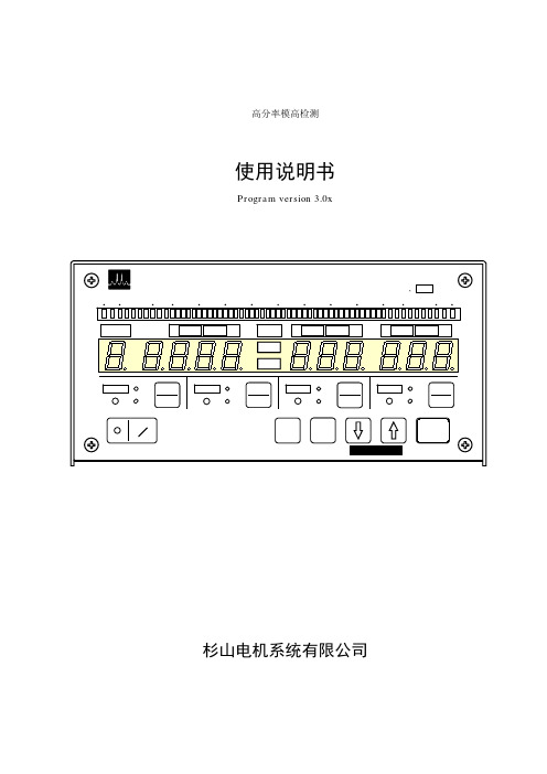
使用说明书
Program version 3.0x
杉山电机系统有限公司
注意
PS-464/462 的目的是减少模具的损坏、产品不良的等不具备。 不能保证完全消除损坏、不具备。 仅使用为 PS-464/462 指定的电源电压 AC100 至 240V。 若超过规定电压,可能会导致火灾。 请勿触摸端子模块。 若触摸端子模块的金属部分,则有触电危险。 请不要对 PS-464/462 进行分解、修理、改造。 当 PS-464/462 发生故障时,请立刻切断电源并停止使用。 若 PS-464/462 发出过热、冒烟、异臭等异常情形, 请立刻切断电源并中断使用。 否则可能导致火灾或触电。
录
1.概要 ..............................................................................1 1-1.性能 ............................................................................1
请勿将 PS-464/462 放置于不稳固的位置。 以免跌落导致受伤。 请勿让 PS-464/462 遭受水或其它液体,不要在潮湿的环境中使用。 以免引起故障、火灾、触电。 在开始使用之前,请先检查。 打开电源后,再确定各个机能正常工作。
记载
功能设定的项目号码与位数位置
“项目号码 nn”为功能设定时使用的号码 nn。nn 表示 2 位数的数值。项目号码 nn-p 的场合,p 为从左 边第 P 位数的数值。P 为 1 之 4。
3.功能 .............................................................................11 3-1.微米微显器的显示 ...............................................................11 3-2.数值补正 .......................................................................12 3-2-1. MANUAL 数值补正............................................................12 3-2-2. QUICK 数值补正.............................................................12 3-2-3. MONITOR ON 转换时的数值补正................................................13 3-3.数值补正后检测 ON、数值补正后检测 OFF ...........................................13 3-4.传感器错误检测 .................................................................13
945gcnl364146_364146
英特尔® 台式机主板D945GCNL产品技术规格2007 年 6 月英特尔®台式机主板 D945GCNL 可能包含某些设计缺陷或错误,一经发现将收入勘误表,并因此可能导致产品与已出版的规格有所差异。
英特尔台式机主板D945GCNL 规格更新中提供了最新的勘误表。
修订记录修订版修订记录日期年 6 月-001 《英特尔®台式机主板 D945GCNL 产品技术规格》第一版 2007 本产品规格仅适用于 BIOS 标识符为 NL94510J.86A 的标准英特尔台式机主板 D945GCNL。
对本规格的改动将首先在英特尔台式机主板 D945GCNL 规格更新中公布,然后再汇编到本文档的修订版中。
本文档提供有关英特尔®产品的信息。
本文档并未授予任何知识产权许可,并未以明示或暗示,或以禁止反言或其它方式授予任何知识产权许可。
除英特尔在其产品的销售条款和条件中声明的责任之外,英特尔概不承担任何其它责任。
并且,英特尔对英特尔产品的销售和/或使用不作任何明示或暗示的担保,包括对产品的特定用途适用性、适销性或对任何专利权、版权或其它知识产权的侵权责任等,均不作担保。
英特尔产品并非设计用于医疗、救生或维生等用途。
英特尔公司可能拥有与所述主题相关的一些专利或正在申请的专利应用、商标、版权或其它知识产权。
提供这些文档及其它材料和信息并不表示英特尔以禁止反言或其它方式对此类专利、商标、版权或其它知识产权提供任何明示或暗示的许可。
英特尔可能随时对产品规格及产品描述作出修改,恕不另行通知。
设计人员不可因本指南中某些功能或指导标注为“保留”或“未定义”,而默认有关缺失信息或功能特性,从而依赖于这些信息。
英特尔保留这些项目用于未来定义,而且对于未来因更改这些项目而可能引起的任何冲突或不兼容性概不负责。
英特尔®台式机主板可能包含某些设计缺陷或错误,一经发现将收入勘误表,并因此可能导致产品与已出版的规格有所差异。
Silicon Labs EM34x Development Kit Quick-Start Gui

QSG100: EM34x Development KitQuick-Start GuideUnpacking the ContentsATTENTION: Observe precautions for handling electrostatic senstive devices.Remove components from their packaging:•Silicon Labs remote control (1)•Silicon Labs EM35x breakout board (1)•EM341-MOD-ANT-C (1)•EM341-MOD-RF-C (1)•EM346-MOD-ANT-C (1) (Installed on EM35x breakout board)•EM346-MOD-RF-C (1)•Silicon Labs Ember Debug Adapter (ISA3) (1)•Packet Trace Port Cable (1)•Data Emulation Interface Cable (1)•Ethernet Cable (1)•USB Cable (1)•USB Power Brick (1)•RF Cable (1)•AAA Batteries (2)Note: It is recommended you watch the EM34x Development Kit training video at /zrctraining before proceeding with the setup of the EM34x Development Kit.Register the Kit on the Support PortalYou must be a registered user of the Silicon Labs Technical Support Portal and EM34x Development Kit must be registered to obtain support and download the latest Silicon Labs development software and stacks.Go to https:///KitRegistration to log in or create an account.Download and InstallationOnce you have created an account and/or are logged in and have completed registration, click the [Take me to latest EmberZNet software] link to access the list of all necessary software.Download and Install the latest version of the following tools:•Ember Desktop•EmberZNet•ISA3 Utilities•IAR Embedded Workbench for ARM (version 7.30)1. Connecting the Ember Debug Adapter (ISA3)1.Confirm the toggle switch is set to the [INT ] position.2.Insert the other end of the Ethernet cable into an Ethernet port on the network. Note : If connecting directly to a developer’s PC, a static IP address must be set. See 2. Configuring Static IP Addresses (optional). It is recommended that you connect the ISA3 to a DHCP port to simplify setup and development.3.Insert one end of the Packet Trace Port cable into the Packet Trace Port of the Debug Adapter.4.Insert one end of the data emulation interface (DEI) cable into the DEI port of the Debug Adapter.Connecting the Ember Debug Adapter (ISA3)Configuring Static IP Addresses (optional) 2. Configuring Static IP Addresses (optional)By default, Ember Debug Adapters are configured to acquire IP addresses using DHCP. If your network environment requires use of static IP addresses, configure the Ember Debug Adapter as follows:1.Disconnect the Ethernet connection from the Ember Debug Adapter.2.Connect one end of the USB cable to the Ember Debug Adapter.3.Connect other end of the USB cable to the PC.4.Run em3xx_isa.exe with these parameters to configure static IP settings.em3xx_isa.exe --admin “ip status IPADDR NETMASK GATEWAY”Replace IPADDR, NETMASK, and GATEWAY with your desired settings.Example: The following command line changes settings to a static IP address of 192.168.1.100 with a netmask of 255.255.255.0 and gateway of 192.168.1.1em3xx_isa --admin “ip static 192.168.1.100 255.255.255.0 192.168.1.1”Result: Success:IP:after reboot Static 182.168.100 255.255.255.0 192.168.1.15.Run em3xx_isa.exe one more time with these parameters to disable DHCP:em3xx_isa.exe --admin “ip dhcp off”Result: Success:IP: (after reboot) DHCP off3. Running the Remote Control Sample ApplicationThere are sample applications for both the remote control (ZRC Controller) and the EM35x breakout board (ZRC Target). The sample applications demonstrate basic RF4CE network and ZRC application functionality. The remote application acts as a generic remote control while the EM35x breakout board acts as a target device. Both devices utilize the ZRC Profile plugin to provide core application-level functionality and the GDP and ZRC plugins to provide ZRC2.0 specific behavior.The target device will automatically start the network. The controller device is responsible for initiating pairing to an existing network. The controller application will disable its receiver automatically to conserve power. This is representative of a sleepy device that is gen-erally a transmit-only device that acts when directed by the user (i.e., a button press). Pressing a button on the controller will result in a command being sent to the target device. The target device will receive the command and send an acknowledgment back to the con-troller.unch Ember Desktop Software.a.Start>All Programs>Ember>Ember Desktop>Ember Desktop2.Enter the Ember ZigBee support portal username obtained from Silicon Labs support and click [Save username] and [Continue].If you don’t have a username, click [Continue] without registration. Once you have a user name, you can register with Help>Regis-ter. If prompted to start the First-Time Setup Wizard, just click [Continue to Ember Desktop].3.Program the remote control with the low-cost-controller application.a.Remove the battery cover and install the batteries in the remote control. Note: The remote control is programmed with thesample application from the factory. Follow the steps below to reprogram the remote control with the sample application.b.Change the ISA Target Power select switch to the EXT position.c.Insert the Packet Trace cable from the ISA3 adapter to the packet trace connector located under the battery cover on the re-mote control.d.Right click on the [EM-ISA-00 adapter] shown in the Adapters window and select [Connect].e.Right click on the [EM-ISA-00 adapter] and select [Upload application].f.Click on the folder to browse for the application.g.Browse to <znet-install-directory>\app\rf4ce\sample-app\low-cost-controller\ and select the [low-cost-controller.s37] file toupload.h.Click [Bootloader]; browse to <znet-install-directory>\tool\bootloader-em341\app-bootloader\; select [app-bootloader.s37].i.Click on the [Erase chip] option and click [OK].j.Wait until application upload is done and click [OK] on the dialog box when complete.k.Unplug the Packet Trace cable from the remote control and replace the battery cover.4.Program the EM35x breakoutboard with the target-zrc20 application.a.Make sure the EM346-MOD-ANT-C module is plugged into the EM35x breakout board.b.Change the ISA Target Power select switch to the INT position. If providing power from USB, the max current limit is 500 mA.Note: If providing USB power from a PC/Laptop USB port, it may not provide enough current to power both the ISA3 adapter and the EM35x board.c.Connect both the Packet Trace cable and DEI cable to the EM35x breakout board.d.Right click on the [EM-ISA-00 adapter] and select [Upload application].e.Click on the folder to browse for the application.f.Browse to <znet-install-directory>\app\rf4ce\sample-app\full-featured-target\ and select the [full-featured-target.s37] file toupload.g.Click on the [Erase chip] option and click [OK].h.Click [Bootloader]; browse to <znet-install-directory>\tool\bootloader-em346\app-bootloader\; select [app-bootloader.s37].i.Wait till application upload is done and click [OK] on the dialog box when complete.5.Set up the Capture session to decode ZRC packets.a.Select File>Preferences and then select [Decoding].b.Select the option [Change the stack version and profile].c.Select [Ember RF4CE stack] and click[Apply] and [OK].6.Start the Capture session.a.Right click the [EM-ISA-00 adapter ] and select [Start capture].7.Pair the devices.a.Press and hold down both the [PAIR] and [STB] buttons on the remote. If a debug cable is attached to the remote, the [PAIR]button cannot be used; the [SETUP] button must be used instead. The Power button should turn red while it is searching for a target device. Release both buttons.b.Press [Button1] on the EM35x breakout board to accept the pairing.c.Once pairing is completed, the Power button on the remote will turn off.8.View Capture activity.a.Press buttons on the remote to see the packet information sent over the air with the Ack from the breakout board.For More Information 4. For More InformationTo better understand Ember Desktop and the network capture activity, refer to /zrctraining.For more information on the development kit hardware, refer to the EM34x User's Guide (UG113).You can also use the Silicon Labs Technical Support Portal at Disclaimer Silicon Laboratories intends to provide customers with the latest, accurate, and in-depth documentation of all peripherals and modules available for system and software implementers using or intending to use the Silicon Laboratories products. Characterization data, available modules and peripherals, memory sizes and memory addresses refer to each specific device, and "Typical" parameters provided can and do vary in different applications. Application examples described herein are for illustrative purposes only. Silicon Laboratories reserves the right to make changes without further notice and limitation to product information, specifications, and descriptions herein, and does not give warranties as to the accuracy or completeness of the included information. Silicon Laboratories shall have no liability for the consequences of use of the information supplied herein. This document does not imply or express copyright licenses granted hereunder to design or fabricate any integrated circuits. The products must not be used within any Life Support System without the specificwritten consent of Silicon Laboratories. A "Life Support System" is any product or system intended to support or sustain life and/or health, which, if it fails, can be reasonably expectedto result in significant personal injury or death. Silicon Laboratories products are generally not intended for military applications. Silicon Laboratories products shall under no circumstances be used in weapons of mass destruction including (but not limited to) nuclear, biological or chemical weapons, or missiles capable of delivering such weapons.Trademark Information Silicon Laboratories Inc., Silicon Laboratories, Silicon Labs, SiLabs and the Silicon Labs logo, CMEMS®, EFM, EFM32, EFR, Energy Micro, Energy Micro logo and combinations thereof, "the world’s most energy friendly microcontrollers", Ember®, EZLink®, EZMac®, EZRadio®, EZRadioPRO®, DSPLL®, ISOmodem ®, Precision32®, ProSLIC®, SiPHY®, USBXpress® and others are trademarks or registered trademarks of Silicon Laboratories Inc. ARM, CORTEX, Cortex-M3 and THUMB are trademarks or registered trademarks of ARM Holdings. Keil is a registered trademark of ARM Limited. All other products or brand names mentioned herein are trademarks of their respective holders.Silicon Laboratories Inc.400 West Cesar Chavez Austin, TX 78701USAdocumentation, software, sourcecode libraries & more. Availablefor Windows, Mac and Linux!/simplicityMCU Portfolio /mcu SW/HW /simplicity Quality /quality Support and Community 。
微电子VSC7440数据手册:L2 L3企业千兆以太网开关,支持10Gbps连接说明书

VSC7440 Datasheet L2/L3 Enterprise Gigabit Ethernet Switch with 10 GbpsLinksMicrosemi HeadquartersOne Enterprise, Aliso Viejo,CA 92656 USAWithin the USA: +1 (800) 713-4113 Outside the USA: +1 (949) 380-6100 Sales: +1 (949) 380-6136Fax: +1 (949) 215-4996Email: *************************** ©2019 Microsemi, a wholly owned subsidiary of Microchip Technology Inc. All rights reserved. Microsemi and the Microsemi logo are registered trademarks of Microsemi Corporation. All other trademarks and service marks are the property of their respective owners. Microsemi makes no warranty, representation, or guarantee regarding the information contained herein or the suitability of its products and services for any particular purpose, nor does Microsemi assume any liability whatsoever arising out of the application or use of any product or circuit. The products sold hereunder and any other products sold by Microsemi have been subject to limited testing and should not be used in conjunction with mission-critical equipment or applications. Any performance specifications are believed to be reliable but are not verified, and Buyer must conduct and complete all performance and other testing of the products, alone and together with, or installed in, any end-products. Buyer shall not rely on any data and performance specifications or parameters provided by Microsemi. It is the Buyer’s responsibility to independently determine suitability of any products and to test and verify the same. The information provided by Microsemi hereunder is provided “as is, where is” and with all faults, and the entire risk associated with such information is entirely with the Buyer. Microsemi does not grant, explicitly or implicitly, to any party any patent rights, licenses, or any other IP rights, whether with regard to such information itself or anything described by such information. Information provided in this document is proprietary to Microsemi, and Microsemi reserves the right to make any changes to the information in this document or to any products and services at any time without notice.About MicrosemiMicrosemi, a wholly owned subsidiary of Microchip Technology Inc. (Nasdaq: MCHP), offers a comprehensive portfolio of semiconductor and system solutions for aerospace & defense, communications, data center and industrial markets. Products include high-performance and radiation-hardened analog mixed-signal integrated circuits, FPGAs, SoCs and ASICs; power management products; timing and synchronization devices and precise time solutions, setting the world's standard for time; voice processing devices; RF solutions; discrete components; enterprise storage and communication solutions, security technologies and scalable anti-tamper products; Ethernet solutions; Power-over-Ethernet ICs andmidspans; as well as custom design capabilities and services. Learn more at .Contents1Revision History . . . . . . . . . . . . . . . . . . . . . . . . . . . . . . . . . . . . . . . . . . . . . . . . . . . . .11.1Revision 4.2 . . . . . . . . . . . . . . . . . . . . . . . . . . . . . . . . . . . . . . . . . . . . . . . . . . . . . . . . . . . . . . . . . . . . . . . 11.2Revision 4.1 . . . . . . . . . . . . . . . . . . . . . . . . . . . . . . . . . . . . . . . . . . . . . . . . . . . . . . . . . . . . . . . . . . . . . . . 11.3Revision 4.0 . . . . . . . . . . . . . . . . . . . . . . . . . . . . . . . . . . . . . . . . . . . . . . . . . . . . . . . . . . . . . . . . . . . . . . . 12Product Overview . . . . . . . . . . . . . . . . . . . . . . . . . . . . . . . . . . . . . . . . . . . . . . . . . . .22.1General Features . . . . . . . . . . . . . . . . . . . . . . . . . . . . . . . . . . . . . . . . . . . . . . . . . . . . . . . . . . . . . . . . . . . 22.1.1Layer2 and Layer3 Forwarding . . . . . . . . . . . . . . . . . . . . . . . . . . . . . . . . . . . . . . . . . . . . . . . . 22.1.2Timing and Synchronization . . . . . . . . . . . . . . . . . . . . . . . . . . . . . . . . . . . . . . . . . . . . . . . . . . . 22.1.3Quality of Service . . . . . . . . . . . . . . . . . . . . . . . . . . . . . . . . . . . . . . . . . . . . . . . . . . . . . . . . . . . 22.1.4Security . . . . . . . . . . . . . . . . . . . . . . . . . . . . . . . . . . . . . . . . . . . . . . . . . . . . . . . . . . . . . . . . . . . 32.1.5Management . . . . . . . . . . . . . . . . . . . . . . . . . . . . . . . . . . . . . . . . . . . . . . . . . . . . . . . . . . . . . . . 32.1.6Product Parameters . . . . . . . . . . . . . . . . . . . . . . . . . . . . . . . . . . . . . . . . . . . . . . . . . . . . . . . . . . 32.2Applications . . . . . . . . . . . . . . . . . . . . . . . . . . . . . . . . . . . . . . . . . . . . . . . . . . . . . . . . . . . . . . . . . . . . . . . 43Functional Descriptions . . . . . . . . . . . . . . . . . . . . . . . . . . . . . . . . . . . . . . . . . . . . . . .53.1Register Notations . . . . . . . . . . . . . . . . . . . . . . . . . . . . . . . . . . . . . . . . . . . . . . . . . . . . . . . . . . . . . . . . . . 63.2Functional Overview . . . . . . . . . . . . . . . . . . . . . . . . . . . . . . . . . . . . . . . . . . . . . . . . . . . . . . . . . . . . . . . . 63.2.1Frame Arrival in Ports and Port Modules . . . . . . . . . . . . . . . . . . . . . . . . . . . . . . . . . . . . . . . . . . 73.2.2Basic Classification . . . . . . . . . . . . . . . . . . . . . . . . . . . . . . . . . . . . . . . . . . . . . . . . . . . . . . . . . . 83.2.3Security and Control Protocol Classification . . . . . . . . . . . . . . . . . . . . . . . . . . . . . . . . . . . . . . . 83.2.4Policing . . . . . . . . . . . . . . . . . . . . . . . . . . . . . . . . . . . . . . . . . . . . . . . . . . . . . . . . . . . . . . . . . . . 93.2.5Layer2 Forwarding . . . . . . . . . . . . . . . . . . . . . . . . . . . . . . . . . . . . . . . . . . . . . . . . . . . . . . . . . . 93.2.6Layer3 Forwarding . . . . . . . . . . . . . . . . . . . . . . . . . . . . . . . . . . . . . . . . . . . . . . . . . . . . . . . . . 103.2.7Shared Queue System and Hierarchical Scheduler . . . . . . . . . . . . . . . . . . . . . . . . . . . . . . . . 113.2.8Rewriter and Frame Departure . . . . . . . . . . . . . . . . . . . . . . . . . . . . . . . . . . . . . . . . . . . . . . . . 113.2.9CPU Port Module . . . . . . . . . . . . . . . . . . . . . . . . . . . . . . . . . . . . . . . . . . . . . . . . . . . . . . . . . . . 123.2.10Synchronous Ethernet and Precision Time Protocol (PTP) . . . . . . . . . . . . . . . . . . . . . . . . . . . 123.2.11CPU Subsystem . . . . . . . . . . . . . . . . . . . . . . . . . . . . . . . . . . . . . . . . . . . . . . . . . . . . . . . . . . . 133.3Frame Headers . . . . . . . . . . . . . . . . . . . . . . . . . . . . . . . . . . . . . . . . . . . . . . . . . . . . . . . . . . . . . . . . . . . 133.3.1Internal Frame Header Placement . . . . . . . . . . . . . . . . . . . . . . . . . . . . . . . . . . . . . . . . . . . . . 133.3.2Internal Frame Header Layout . . . . . . . . . . . . . . . . . . . . . . . . . . . . . . . . . . . . . . . . . . . . . . . . . 143.3.3VStaX Header . . . . . . . . . . . . . . . . . . . . . . . . . . . . . . . . . . . . . . . . . . . . . . . . . . . . . . . . . . . . . 203.4Port Numbering and Mappings . . . . . . . . . . . . . . . . . . . . . . . . . . . . . . . . . . . . . . . . . . . . . . . . . . . . . . . 243.4.1Supported SerDes Interfaces . . . . . . . . . . . . . . . . . . . . . . . . . . . . . . . . . . . . . . . . . . . . . . . . . 253.4.2Dual-Media Mode . . . . . . . . . . . . . . . . . . . . . . . . . . . . . . . . . . . . . . . . . . . . . . . . . . . . . . . . . . 263.4.310G Modes . . . . . . . . . . . . . . . . . . . . . . . . . . . . . . . . . . . . . . . . . . . . . . . . . . . . . . . . . . . . . . . 263.4.4Logical Port Numbers . . . . . . . . . . . . . . . . . . . . . . . . . . . . . . . . . . . . . . . . . . . . . . . . . . . . . . . 273.5SERDES1G . . . . . . . . . . . . . . . . . . . . . . . . . . . . . . . . . . . . . . . . . . . . . . . . . . . . . . . . . . . . . . . . . . . . . . 283.6SERDES6G . . . . . . . . . . . . . . . . . . . . . . . . . . . . . . . . . . . . . . . . . . . . . . . . . . . . . . . . . . . . . . . . . . . . . . 283.7SERDES10G . . . . . . . . . . . . . . . . . . . . . . . . . . . . . . . . . . . . . . . . . . . . . . . . . . . . . . . . . . . . . . . . . . . . . 283.8Copper Transceivers . . . . . . . . . . . . . . . . . . . . . . . . . . . . . . . . . . . . . . . . . . . . . . . . . . . . . . . . . . . . . . . 293.8.1Register Access . . . . . . . . . . . . . . . . . . . . . . . . . . . . . . . . . . . . . . . . . . . . . . . . . . . . . . . . . . . . 293.8.2Cat5 Twisted Pair Media Interface . . . . . . . . . . . . . . . . . . . . . . . . . . . . . . . . . . . . . . . . . . . . . 303.8.3Wake-On-LAN and SecureOn . . . . . . . . . . . . . . . . . . . . . . . . . . . . . . . . . . . . . . . . . . . . . . . . . 323.8.4Ethernet Inline Powered Devices . . . . . . . . . . . . . . . . . . . . . . . . . . . . . . . . . . . . . . . . . . . . . . 333.8.5IEEE 802.3af PoE Support . . . . . . . . . . . . . . . . . . . . . . . . . . . . . . . . . . . . . . . . . . . . . . . . . . . 343.8.6ActiPHY™ Power Management . . . . . . . . . . . . . . . . . . . . . . . . . . . . . . . . . . . . . . . . . . . . . . . 343.8.7Testing Features . . . . . . . . . . . . . . . . . . . . . . . . . . . . . . . . . . . . . . . . . . . . . . . . . . . . . . . . . . . 353.8.8VeriPHY™ Cable Diagnostics . . . . . . . . . . . . . . . . . . . . . . . . . . . . . . . . . . . . . . . . . . . . . . . . . 373.9DEV1G and DEV2G5 Port Modules . . . . . . . . . . . . . . . . . . . . . . . . . . . . . . . . . . . . . . . . . . . . . . . . . . . 373.9.1MAC . . . . . . . . . . . . . . . . . . . . . . . . . . . . . . . . . . . . . . . . . . . . . . . . . . . . . . . . . . . . . . . . . . . . . 373.9.2Half-Duplex Mode . . . . . . . . . . . . . . . . . . . . . . . . . . . . . . . . . . . . . . . . . . . . . . . . . . . . . . . . . . 393.9.3Physical Coding Sublayer (PCS) . . . . . . . . . . . . . . . . . . . . . . . . . . . . . . . . . . . . . . . . . . . . . . . 403.9.4Port Statistics . . . . . . . . . . . . . . . . . . . . . . . . . . . . . . . . . . . . . . . . . . . . . . . . . . . . . . . . . . . . . . 43 3.10DEV10G Port Module . . . . . . . . . . . . . . . . . . . . . . . . . . . . . . . . . . . . . . . . . . . . . . . . . . . . . . . . . . . . . . 433.10.1MAC . . . . . . . . . . . . . . . . . . . . . . . . . . . . . . . . . . . . . . . . . . . . . . . . . . . . . . . . . . . . . . . . . . . . . 433.10.2Physical Coding Sublayer (PCS) . . . . . . . . . . . . . . . . . . . . . . . . . . . . . . . . . . . . . . . . . . . . . . . 463.10.3Port Statistics . . . . . . . . . . . . . . . . . . . . . . . . . . . . . . . . . . . . . . . . . . . . . . . . . . . . . . . . . . . . . . 49 3.11Assembler . . . . . . . . . . . . . . . . . . . . . . . . . . . . . . . . . . . . . . . . . . . . . . . . . . . . . . . . . . . . . . . . . . . . . . . 503.11.1Setting Up a Port in the Assembler . . . . . . . . . . . . . . . . . . . . . . . . . . . . . . . . . . . . . . . . . . . . . 503.11.2Setting Up a Port for Frame Injection . . . . . . . . . . . . . . . . . . . . . . . . . . . . . . . . . . . . . . . . . . . 513.11.3Setting Up MAC Control Sublayer PAUSE Frame Detection . . . . . . . . . . . . . . . . . . . . . . . . . 523.11.4Setting Up PFC . . . . . . . . . . . . . . . . . . . . . . . . . . . . . . . . . . . . . . . . . . . . . . . . . . . . . . . . . . . . 533.11.5Setting Up Assembler Port Statistics . . . . . . . . . . . . . . . . . . . . . . . . . . . . . . . . . . . . . . . . . . . . 533.11.6Setting Up the Loopback Path . . . . . . . . . . . . . . . . . . . . . . . . . . . . . . . . . . . . . . . . . . . . . . . . . 54 3.12Versatile Content-Aware Processor (VCAP) . . . . . . . . . . . . . . . . . . . . . . . . . . . . . . . . . . . . . . . . . . . . . 553.12.1Configuring VCAP . . . . . . . . . . . . . . . . . . . . . . . . . . . . . . . . . . . . . . . . . . . . . . . . . . . . . . . . . . 553.12.2Wide VCAP Entries and Actions . . . . . . . . . . . . . . . . . . . . . . . . . . . . . . . . . . . . . . . . . . . . . . . 583.12.3Individual VCAPs . . . . . . . . . . . . . . . . . . . . . . . . . . . . . . . . . . . . . . . . . . . . . . . . . . . . . . . . . . . 593.12.4VCAP Programming Examples . . . . . . . . . . . . . . . . . . . . . . . . . . . . . . . . . . . . . . . . . . . . . . . . 65 3.13Pipeline Points . . . . . . . . . . . . . . . . . . . . . . . . . . . . . . . . . . . . . . . . . . . . . . . . . . . . . . . . . . . . . . . . . . . . 673.13.1Pipeline Definitions . . . . . . . . . . . . . . . . . . . . . . . . . . . . . . . . . . . . . . . . . . . . . . . . . . . . . . . . . 68 3.14Analyzer . . . . . . . . . . . . . . . . . . . . . . . . . . . . . . . . . . . . . . . . . . . . . . . . . . . . . . . . . . . . . . . . . . . . . . . . . 703.14.1Initializing the Analyzer . . . . . . . . . . . . . . . . . . . . . . . . . . . . . . . . . . . . . . . . . . . . . . . . . . . . . . 71 3.15VCAP CLM Keys and Actions . . . . . . . . . . . . . . . . . . . . . . . . . . . . . . . . . . . . . . . . . . . . . . . . . . . . . . . . 713.15.1Keys Overview . . . . . . . . . . . . . . . . . . . . . . . . . . . . . . . . . . . . . . . . . . . . . . . . . . . . . . . . . . . . . 713.15.2VCAP CLM X1 Key Details . . . . . . . . . . . . . . . . . . . . . . . . . . . . . . . . . . . . . . . . . . . . . . . . . . . 743.15.3VCAP CLM X2 Key Details . . . . . . . . . . . . . . . . . . . . . . . . . . . . . . . . . . . . . . . . . . . . . . . . . . . 753.15.4VCAP CLM X4 Key Details . . . . . . . . . . . . . . . . . . . . . . . . . . . . . . . . . . . . . . . . . . . . . . . . . . . 783.15.5VCAP CLM X8 Key Details . . . . . . . . . . . . . . . . . . . . . . . . . . . . . . . . . . . . . . . . . . . . . . . . . . . 813.15.6VCAP CLM X16 Key Details . . . . . . . . . . . . . . . . . . . . . . . . . . . . . . . . . . . . . . . . . . . . . . . . . . 873.15.7VCAP CLM Actions . . . . . . . . . . . . . . . . . . . . . . . . . . . . . . . . . . . . . . . . . . . . . . . . . . . . . . . . . 92 3.16Analyzer Classifier . . . . . . . . . . . . . . . . . . . . . . . . . . . . . . . . . . . . . . . . . . . . . . . . . . . . . . . . . . . . . . . . 1033.16.1Basic Classifier . . . . . . . . . . . . . . . . . . . . . . . . . . . . . . . . . . . . . . . . . . . . . . . . . . . . . . . . . . . 1033.16.2VCAP CLM Processing . . . . . . . . . . . . . . . . . . . . . . . . . . . . . . . . . . . . . . . . . . . . . . . . . . . . . 1153.16.3QoS Mapping Table . . . . . . . . . . . . . . . . . . . . . . . . . . . . . . . . . . . . . . . . . . . . . . . . . . . . . . . . 1223.16.4Analyzer Classifier Diagnostics . . . . . . . . . . . . . . . . . . . . . . . . . . . . . . . . . . . . . . . . . . . . . . . 124 3.17VLAN and MSTP . . . . . . . . . . . . . . . . . . . . . . . . . . . . . . . . . . . . . . . . . . . . . . . . . . . . . . . . . . . . . . . . . 1243.17.1Private VLAN . . . . . . . . . . . . . . . . . . . . . . . . . . . . . . . . . . . . . . . . . . . . . . . . . . . . . . . . . . . . . 1263.17.2VLAN Pseudo Code . . . . . . . . . . . . . . . . . . . . . . . . . . . . . . . . . . . . . . . . . . . . . . . . . . . . . . . 126 3.18VCAP LPM: Keys and Action . . . . . . . . . . . . . . . . . . . . . . . . . . . . . . . . . . . . . . . . . . . . . . . . . . . . . . . . 1313.18.1VCAP LPM SGL_IP4 Key Details . . . . . . . . . . . . . . . . . . . . . . . . . . . . . . . . . . . . . . . . . . . . . 1323.18.2VCAP LPM DBL_IP4 Key Details . . . . . . . . . . . . . . . . . . . . . . . . . . . . . . . . . . . . . . . . . . . . . 1323.18.3VCAP LPM SGL_IP6 Key Details . . . . . . . . . . . . . . . . . . . . . . . . . . . . . . . . . . . . . . . . . . . . . 1323.18.4VCAP LPM DBL_IP6 Key Details . . . . . . . . . . . . . . . . . . . . . . . . . . . . . . . . . . . . . . . . . . . . . 1323.18.5VCAP LPM Actions . . . . . . . . . . . . . . . . . . . . . . . . . . . . . . . . . . . . . . . . . . . . . . . . . . . . . . . . 132 3.19IP Processing . . . . . . . . . . . . . . . . . . . . . . . . . . . . . . . . . . . . . . . . . . . . . . . . . . . . . . . . . . . . . . . . . . . . 1343.19.1IP Source/Destination Guard . . . . . . . . . . . . . . . . . . . . . . . . . . . . . . . . . . . . . . . . . . . . . . . . . 1343.19.2IP Routing . . . . . . . . . . . . . . . . . . . . . . . . . . . . . . . . . . . . . . . . . . . . . . . . . . . . . . . . . . . . . . . 1363.19.3Statistics . . . . . . . . . . . . . . . . . . . . . . . . . . . . . . . . . . . . . . . . . . . . . . . . . . . . . . . . . . . . . . . . 1483.19.4IGMP/MLD Snooping Switch . . . . . . . . . . . . . . . . . . . . . . . . . . . . . . . . . . . . . . . . . . . . . . . . . 150 3.20VCAP IS2 Keys and Actions . . . . . . . . . . . . . . . . . . . . . . . . . . . . . . . . . . . . . . . . . . . . . . . . . . . . . . . . 1503.20.1VCAP IS2 Keys . . . . . . . . . . . . . . . . . . . . . . . . . . . . . . . . . . . . . . . . . . . . . . . . . . . . . . . . . . . 1513.20.2VCAP IS2 Actions . . . . . . . . . . . . . . . . . . . . . . . . . . . . . . . . . . . . . . . . . . . . . . . . . . . . . . . . . 157 3.21Analyzer Access Control Lists . . . . . . . . . . . . . . . . . . . . . . . . . . . . . . . . . . . . . . . . . . . . . . . . . . . . . . . 1603.21.1VCAP IS2 . . . . . . . . . . . . . . . . . . . . . . . . . . . . . . . . . . . . . . . . . . . . . . . . . . . . . . . . . . . . . . . 1613.21.2Analyzer Access Control List Frame Rewriting . . . . . . . . . . . . . . . . . . . . . . . . . . . . . . . . . . . 167 3.22Analyzer Layer2 Forwarding and Learning . . . . . . . . . . . . . . . . . . . . . . . . . . . . . . . . . . . . . . . . . . . . . 1703.22.1Analyzer MAC Table . . . . . . . . . . . . . . . . . . . . . . . . . . . . . . . . . . . . . . . . . . . . . . . . . . . . . . . 1703.22.2MAC Table Updates . . . . . . . . . . . . . . . . . . . . . . . . . . . . . . . . . . . . . . . . . . . . . . . . . . . . . . . 1723.22.3CPU Access to MAC Table . . . . . . . . . . . . . . . . . . . . . . . . . . . . . . . . . . . . . . . . . . . . . . . . . . 1723.22.4SCAN Command . . . . . . . . . . . . . . . . . . . . . . . . . . . . . . . . . . . . . . . . . . . . . . . . . . . . . . . . . . 1763.22.5Forwarding Lookups . . . . . . . . . . . . . . . . . . . . . . . . . . . . . . . . . . . . . . . . . . . . . . . . . . . . . . . 1783.22.6Source Check and Automated Learning . . . . . . . . . . . . . . . . . . . . . . . . . . . . . . . . . . . . . . . . 1803.22.7Automated Aging (AUTOAGE) . . . . . . . . . . . . . . . . . . . . . . . . . . . . . . . . . . . . . . . . . . . . . . . 1833.22.8Interrupt Handling . . . . . . . . . . . . . . . . . . . . . . . . . . . . . . . . . . . . . . . . . . . . . . . . . . . . . . . . . 184 3.23Analyzer Access Control Forwarding, Policing, and Statistics . . . . . . . . . . . . . . . . . . . . . . . . . . . . . . . 1853.23.1Mask Handling . . . . . . . . . . . . . . . . . . . . . . . . . . . . . . . . . . . . . . . . . . . . . . . . . . . . . . . . . . . . 1853.23.2Policing . . . . . . . . . . . . . . . . . . . . . . . . . . . . . . . . . . . . . . . . . . . . . . . . . . . . . . . . . . . . . . . . . 1903.23.3Analyzer Statistics . . . . . . . . . . . . . . . . . . . . . . . . . . . . . . . . . . . . . . . . . . . . . . . . . . . . . . . . . 1983.23.4Analyzer sFlow Sampling . . . . . . . . . . . . . . . . . . . . . . . . . . . . . . . . . . . . . . . . . . . . . . . . . . . 2053.23.5Mirroring . . . . . . . . . . . . . . . . . . . . . . . . . . . . . . . . . . . . . . . . . . . . . . . . . . . . . . . . . . . . . . . . 206 3.24Shared Queue System and Hierarchical Scheduler . . . . . . . . . . . . . . . . . . . . . . . . . . . . . . . . . . . . . . . 2083.24.1Analyzer Result . . . . . . . . . . . . . . . . . . . . . . . . . . . . . . . . . . . . . . . . . . . . . . . . . . . . . . . . . . . 2103.24.2Buffer Control . . . . . . . . . . . . . . . . . . . . . . . . . . . . . . . . . . . . . . . . . . . . . . . . . . . . . . . . . . . . 2103.24.3Forwarding . . . . . . . . . . . . . . . . . . . . . . . . . . . . . . . . . . . . . . . . . . . . . . . . . . . . . . . . . . . . . . . 2113.24.4Congestion Control . . . . . . . . . . . . . . . . . . . . . . . . . . . . . . . . . . . . . . . . . . . . . . . . . . . . . . . . 2133.24.5Queue Mapping . . . . . . . . . . . . . . . . . . . . . . . . . . . . . . . . . . . . . . . . . . . . . . . . . . . . . . . . . . . 2193.24.6Queue Congestion Control . . . . . . . . . . . . . . . . . . . . . . . . . . . . . . . . . . . . . . . . . . . . . . . . . . 2233.24.7Scheduling . . . . . . . . . . . . . . . . . . . . . . . . . . . . . . . . . . . . . . . . . . . . . . . . . . . . . . . . . . . . . . . 2253.24.8Queue System Initialization . . . . . . . . . . . . . . . . . . . . . . . . . . . . . . . . . . . . . . . . . . . . . . . . . . 2293.24.9Miscellaneous Features . . . . . . . . . . . . . . . . . . . . . . . . . . . . . . . . . . . . . . . . . . . . . . . . . . . . . 229 3.25Automatic Frame Injector . . . . . . . . . . . . . . . . . . . . . . . . . . . . . . . . . . . . . . . . . . . . . . . . . . . . . . . . . . . 2323.25.1Injection Tables . . . . . . . . . . . . . . . . . . . . . . . . . . . . . . . . . . . . . . . . . . . . . . . . . . . . . . . . . . . 2333.25.2Frame Table . . . . . . . . . . . . . . . . . . . . . . . . . . . . . . . . . . . . . . . . . . . . . . . . . . . . . . . . . . . . . 2343.25.3Delay Triggered Injection . . . . . . . . . . . . . . . . . . . . . . . . . . . . . . . . . . . . . . . . . . . . . . . . . . . . 2343.25.4Timer Triggered Injection . . . . . . . . . . . . . . . . . . . . . . . . . . . . . . . . . . . . . . . . . . . . . . . . . . . . 2383.25.5Injection Queues . . . . . . . . . . . . . . . . . . . . . . . . . . . . . . . . . . . . . . . . . . . . . . . . . . . . . . . . . . 2443.25.6Adding Injection Frame . . . . . . . . . . . . . . . . . . . . . . . . . . . . . . . . . . . . . . . . . . . . . . . . . . . . . 2443.25.7Starting Injection . . . . . . . . . . . . . . . . . . . . . . . . . . . . . . . . . . . . . . . . . . . . . . . . . . . . . . . . . . 2453.25.8Stopping Injection . . . . . . . . . . . . . . . . . . . . . . . . . . . . . . . . . . . . . . . . . . . . . . . . . . . . . . . . . 2453.25.9Removing Injection Frames . . . . . . . . . . . . . . . . . . . . . . . . . . . . . . . . . . . . . . . . . . . . . . . . . . 2453.25.10Port Parameters . . . . . . . . . . . . . . . . . . . . . . . . . . . . . . . . . . . . . . . . . . . . . . . . . . . . . . . . . . 245 3.26Rewriter . . . . . . . . . . . . . . . . . . . . . . . . . . . . . . . . . . . . . . . . . . . . . . . . . . . . . . . . . . . . . . . . . . . . . . . . 2463.26.1Rewriter Operation . . . . . . . . . . . . . . . . . . . . . . . . . . . . . . . . . . . . . . . . . . . . . . . . . . . . . . . . 2463.26.2Supported Ports . . . . . . . . . . . . . . . . . . . . . . . . . . . . . . . . . . . . . . . . . . . . . . . . . . . . . . . . . . . 2463.26.3Supported Frame Formats . . . . . . . . . . . . . . . . . . . . . . . . . . . . . . . . . . . . . . . . . . . . . . . . . . 2473.26.4Rewriter Initialization . . . . . . . . . . . . . . . . . . . . . . . . . . . . . . . . . . . . . . . . . . . . . . . . . . . . . . . 2473.26.5VCAP_ES0 Lookup . . . . . . . . . . . . . . . . . . . . . . . . . . . . . . . . . . . . . . . . . . . . . . . . . . . . . . . . 2473.26.6Mapping Tables . . . . . . . . . . . . . . . . . . . . . . . . . . . . . . . . . . . . . . . . . . . . . . . . . . . . . . . . . . . 2593.26.7VLAN Editing . . . . . . . . . . . . . . . . . . . . . . . . . . . . . . . . . . . . . . . . . . . . . . . . . . . . . . . . . . . . . 2613.26.8DSCP Remarking . . . . . . . . . . . . . . . . . . . . . . . . . . . . . . . . . . . . . . . . . . . . . . . . . . . . . . . . . 2663.26.9VStaX Header Insertion . . . . . . . . . . . . . . . . . . . . . . . . . . . . . . . . . . . . . . . . . . . . . . . . . . . . . 2673.26.10Forwarding to GCPU . . . . . . . . . . . . . . . . . . . . . . . . . . . . . . . . . . . . . . . . . . . . . . . . . . . . . . . 2673.26.11Layer 3 Routing . . . . . . . . . . . . . . . . . . . . . . . . . . . . . . . . . . . . . . . . . . . . . . . . . . . . . . . . . . . 2693.26.12Mirror Frames . . . . . . . . . . . . . . . . . . . . . . . . . . . . . . . . . . . . . . . . . . . . . . . . . . . . . . . . . . . . 2693.26.13Internal Frame Header Insertion . . . . . . . . . . . . . . . . . . . . . . . . . . . . . . . . . . . . . . . . . . . . . . 2703.26.14Frame Injection from Internal CPU . . . . . . . . . . . . . . . . . . . . . . . . . . . . . . . . . . . . . . . . . . . . 271 3.27Disassembler . . . . . . . . . . . . . . . . . . . . . . . . . . . . . . . . . . . . . . . . . . . . . . . . . . . . . . . . . . . . . . . . . . . . 2723.27.1Setting Up Ports . . . . . . . . . . . . . . . . . . . . . . . . . . . . . . . . . . . . . . . . . . . . . . . . . . . . . . . . . . 2723.27.2Maintaining the Cell Buffer . . . . . . . . . . . . . . . . . . . . . . . . . . . . . . . . . . . . . . . . . . . . . . . . . . 2733.27.3Setting Up MAC Control Sublayer PAUSE Function . . . . . . . . . . . . . . . . . . . . . . . . . . . . . . . 2733.27.4Setting up Flow Control in Half-Duplex Mode . . . . . . . . . . . . . . . . . . . . . . . . . . . . . . . . . . . . 2743.27.5Setting Up Frame Aging . . . . . . . . . . . . . . . . . . . . . . . . . . . . . . . . . . . . . . . . . . . . . . . . . . . . 2743.27.6Setting Up Transmit Data Rate Limiting . . . . . . . . . . . . . . . . . . . . . . . . . . . . . . . . . . . . . . . . 2753.27.7Error Detection . . . . . . . . . . . . . . . . . . . . . . . . . . . . . . . . . . . . . . . . . . . . . . . . . . . . . . . . . . . 2773.28Layer 1 Timing . . . . . . . . . . . . . . . . . . . . . . . . . . . . . . . . . . . . . . . . . . . . . . . . . . . . . . . . . . . . . . . . . . . 2773.29Hardware Time Stamping . . . . . . . . . . . . . . . . . . . . . . . . . . . . . . . . . . . . . . . . . . . . . . . . . . . . . . . . . . 2813.29.1One-Step Functions . . . . . . . . . . . . . . . . . . . . . . . . . . . . . . . . . . . . . . . . . . . . . . . . . . . . . . . . 2833.29.2Calculation Overview . . . . . . . . . . . . . . . . . . . . . . . . . . . . . . . . . . . . . . . . . . . . . . . . . . . . . . . 2843.29.3Detecting Calculation Issues . . . . . . . . . . . . . . . . . . . . . . . . . . . . . . . . . . . . . . . . . . . . . . . . . 2853.29.4Two-Step Functions . . . . . . . . . . . . . . . . . . . . . . . . . . . . . . . . . . . . . . . . . . . . . . . . . . . . . . . . 2853.29.5Time of Day Time Stamping . . . . . . . . . . . . . . . . . . . . . . . . . . . . . . . . . . . . . . . . . . . . . . . . . 2853.29.6Time of Day Generation . . . . . . . . . . . . . . . . . . . . . . . . . . . . . . . . . . . . . . . . . . . . . . . . . . . . 2863.29.7Multiple PTP Time Domains . . . . . . . . . . . . . . . . . . . . . . . . . . . . . . . . . . . . . . . . . . . . . . . . . 2873.29.8Register Interface to 1588 Functions . . . . . . . . . . . . . . . . . . . . . . . . . . . . . . . . . . . . . . . . . . . 2873.29.9Configuring I/O Delays . . . . . . . . . . . . . . . . . . . . . . . . . . . . . . . . . . . . . . . . . . . . . . . . . . . . . 2893.30VRAP Engine . . . . . . . . . . . . . . . . . . . . . . . . . . . . . . . . . . . . . . . . . . . . . . . . . . . . . . . . . . . . . . . . . . . . 2893.30.1VRAP Request Frame Format . . . . . . . . . . . . . . . . . . . . . . . . . . . . . . . . . . . . . . . . . . . . . . . . 2903.30.2VRAP Response Frame Format . . . . . . . . . . . . . . . . . . . . . . . . . . . . . . . . . . . . . . . . . . . . . . 2913.30.3VRAP Header Format . . . . . . . . . . . . . . . . . . . . . . . . . . . . . . . . . . . . . . . . . . . . . . . . . . . . . . 2913.30.4VRAP READ Command . . . . . . . . . . . . . . . . . . . . . . . . . . . . . . . . . . . . . . . . . . . . . . . . . . . . 2913.30.5VRAP READ-MODIFY-WRITE Command . . . . . . . . . . . . . . . . . . . . . . . . . . . . . . . . . . . . . . 2923.30.6VRAP IDLE Command . . . . . . . . . . . . . . . . . . . . . . . . . . . . . . . . . . . . . . . . . . . . . . . . . . . . . 2923.30.7VRAP PAUSE Command . . . . . . . . . . . . . . . . . . . . . . . . . . . . . . . . . . . . . . . . . . . . . . . . . . . 2923.31Energy Efficient Ethernet . . . . . . . . . . . . . . . . . . . . . . . . . . . . . . . . . . . . . . . . . . . . . . . . . . . . . . . . . . . 2933.32CPU Injection and Extraction . . . . . . . . . . . . . . . . . . . . . . . . . . . . . . . . . . . . . . . . . . . . . . . . . . . . . . . . 2943.32.1Frame Injection . . . . . . . . . . . . . . . . . . . . . . . . . . . . . . . . . . . . . . . . . . . . . . . . . . . . . . . . . . . 2943.32.2Frame Extraction . . . . . . . . . . . . . . . . . . . . . . . . . . . . . . . . . . . . . . . . . . . . . . . . . . . . . . . . . . 2953.32.3Forwarding to CPU . . . . . . . . . . . . . . . . . . . . . . . . . . . . . . . . . . . . . . . . . . . . . . . . . . . . . . . . 2953.32.4Automatic Frame Injection (AFI) . . . . . . . . . . . . . . . . . . . . . . . . . . . . . . . . . . . . . . . . . . . . . . 2953.33Priority-Based Flow Control (PFC) . . . . . . . . . . . . . . . . . . . . . . . . . . . . . . . . . . . . . . . . . . . . . . . . . . . . 2963.33.1PFC Pause Frame Generation . . . . . . . . . . . . . . . . . . . . . . . . . . . . . . . . . . . . . . . . . . . . . . . 2963.33.2PFC Frame Reception . . . . . . . . . . . . . . . . . . . . . . . . . . . . . . . . . . . . . . . . . . . . . . . . . . . . . . 2973.34Protection Switching . . . . . . . . . . . . . . . . . . . . . . . . . . . . . . . . . . . . . . . . . . . . . . . . . . . . . . . . . . . . . . 2973.34.1Ethernet Ring Protection Switching . . . . . . . . . . . . . . . . . . . . . . . . . . . . . . . . . . . . . . . . . . . . 2983.34.2Link Aggregation . . . . . . . . . . . . . . . . . . . . . . . . . . . . . . . . . . . . . . . . . . . . . . . . . . . . . . . . . . 3013.34.3Port Protection Switching . . . . . . . . . . . . . . . . . . . . . . . . . . . . . . . . . . . . . . . . . . . . . . . . . . . 3013.35Low Power Mode . . . . . . . . . . . . . . . . . . . . . . . . . . . . . . . . . . . . . . . . . . . . . . . . . . . . . . . . . . . . . . . . . 3013.35.1One-Time Configurations for Low Power Mode . . . . . . . . . . . . . . . . . . . . . . . . . . . . . . . . . . 3013.35.2General Considerations in Low Power Mode . . . . . . . . . . . . . . . . . . . . . . . . . . . . . . . . . . . . 3023.36Clocking and Reset . . . . . . . . . . . . . . . . . . . . . . . . . . . . . . . . . . . . . . . . . . . . . . . . . . . . . . . . . . . . . . . 3023.36.1Pin Strapping . . . . . . . . . . . . . . . . . . . . . . . . . . . . . . . . . . . . . . . . . . . . . . . . . . . . . . . . . . . . . 3034VCore-III System and CPU Interfaces . . . . . . . . . . . . . . . . . . . . . . . . . . . . . . . . . .3054.1VCore-III Configurations . . . . . . . . . . . . . . . . . . . . . . . . . . . . . . . . . . . . . . . . . . . . . . . . . . . . . . . . . . . 3064.2Clocking and Reset . . . . . . . . . . . . . . . . . . . . . . . . . . . . . . . . . . . . . . . . . . . . . . . . . . . . . . . . . . . . . . . 3064.2.1Watchdog Timer . . . . . . . . . . . . . . . . . . . . . . . . . . . . . . . . . . . . . . . . . . . . . . . . . . . . . . . . . . 3074.3Shared Bus . . . . . . . . . . . . . . . . . . . . . . . . . . . . . . . . . . . . . . . . . . . . . . . . . . . . . . . . . . . . . . . . . . . . . 3074.3.1VCore-III Shared Bus Arbitration . . . . . . . . . . . . . . . . . . . . . . . . . . . . . . . . . . . . . . . . . . . . . . 3094.3.2Chip Register Region . . . . . . . . . . . . . . . . . . . . . . . . . . . . . . . . . . . . . . . . . . . . . . . . . . . . . . 3094.3.3SI Flash Region . . . . . . . . . . . . . . . . . . . . . . . . . . . . . . . . . . . . . . . . . . . . . . . . . . . . . . . . . . . 3104.3.4DDR3/DDR3L Region . . . . . . . . . . . . . . . . . . . . . . . . . . . . . . . . . . . . . . . . . . . . . . . . . . . . . . 3114.3.5PCIe Region . . . . . . . . . . . . . . . . . . . . . . . . . . . . . . . . . . . . . . . . . . . . . . . . . . . . . . . . . . . . . 3114.4VCore-III CPU . . . . . . . . . . . . . . . . . . . . . . . . . . . . . . . . . . . . . . . . . . . . . . . . . . . . . . . . . . . . . . . . . . . 3114.4.1Little Endian and Big Endian Support . . . . . . . . . . . . . . . . . . . . . . . . . . . . . . . . . . . . . . . . . . 3114.4.2Software Debug and Development . . . . . . . . . . . . . . . . . . . . . . . . . . . . . . . . . . . . . . . . . . . . 3114.5External CPU Support . . . . . . . . . . . . . . . . . . . . . . . . . . . . . . . . . . . . . . . . . . . . . . . . . . . . . . . . . . . . . 3114.5.1Register Access and Multimaster Systems . . . . . . . . . . . . . . . . . . . . . . . . . . . . . . . . . . . . . . 3124.5.2Serial Interface in Slave Mode . . . . . . . . . . . . . . . . . . . . . . . . . . . . . . . . . . . . . . . . . . . . . . . . 312。
A43L3616资料
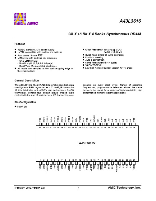
General Description
The A43L3616 is 134,217,728 bits synchronous high data rate Dynamic RAM organized as 4 X 2,097,152 words by 16 bits, fabricated with AMIC’s high performance CMOS technology. Synchronous design allows precise cycle control with the use of system clock. I/O transactions are possible on every clock cycle. Range of operating frequencies, programmable latencies allows the same device to be useful for a variety of high bandwidth, high performance memory system applications.
Pin Configuration
n TSOP (II)
VDDQ
VSSQ
DQ14
DQ13
DQ11
UDQM
VDDQ
VSSQ
DQ15
DQ12
DQ10
CKE
VSS
VSS
DQ8
54 53 52 51 50 49 48 47 46 45 44 43 42 41 40 39 38 37 36 35 34 33 32 31 30 29 28
元器件交易网
A43L3616
2M X 16 Bit X 4 Banks Synchronous DRAM
MEMORY存储芯片TMS320C6414EZLZA6E3中文规格书
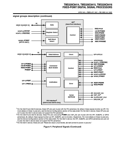
TMS320C6414, TMS320C6415, TMS320C6416FIXED-POINT DIGITAL SIGNAL PROCESSORSSPRS146N − FEBRUARY 2001 − REVISED MAY 2005signal groups description (continued)HHWIL/PTRDY HCNTL0/PSTOP HCNTL1/PDEVSELHD[31:0]/AD[31:0]HAS/PPARHR/W/PCBE2HCS/PPERRHDS1/PSERRHDS2/PCBE1HRDY/PIRDYHINT/PFRAME (HPI16 ONLY)†For the C6415 and C6416 devices, these HPI pins are muxed with the PCI peripheral. By default, these signals function as HPI. For more details on these muxed pins, see the Device Configurations section of this data sheet. For the C6414 device, these HPI pins are not muxed; the C6414 device does not support the PCI peripheral.‡For the C6415 and C6416 devices, these PCI pins (excluding PCBE0 and XSP_CS) are muxed with the HPI, McBSP2, or GPIO peripherals. By default, these signals function as HPI, McBSP2, and no function, respectively. For more details on these muxed pins,see the Device Configurations section of this data sheet. For the C6414 device, the HPI, McBSP2, and GPIO peripheral pins are not muxed; the C6414 device does not support the PCI peripheral.§For the C6414 device, these pins are “Reserved (leave unconnected, do not connect to power or ground).”GP14/PCLK HINT/PFRAME GP13/PINTA HAS/PPARGP15/PRSTHRDY/PIRDYHCNTL0/PSTOPHHWIL/PTRDYGP9/PIDSEL HCNTL1/PDEVSEL HDS1/PSERRDX2/XSP_DO XSP_CS §CLKX2/XSP_CLK DR2/XSP_DIHCS/PPERRFigure 4. Peripheral Signals (Continued)TMS320C6414, TMS320C6415, TMS320C6416FIXED-POINT DIGITAL SIGNAL PROCESSORSSPRS146N − FEBRUARY 2001 − REVISED MAY 2005signal groups description (continued)CLKX0FSX0DX0CLKR0FSR0DR0CLKS0CLKX1/URADDR4†FSX1/UXADDR3†DX1/UXADDR4†CLKR1/URADDR2†FSR1/UXADDR2†DR1/UXADDR1†CLKS1/URADDR3†CLKX2/XSP_CLK †FSX2DX2/XSP_DO †CLKR2FSR2DR2/XSP_DI †CLKS2/GP8‡†For the C6415 and C6416 devices, these McBSP2 and McBSP1 pins are muxed with the PCI and UTOPIA peripherals, respectively.By default, these signals function as McBSP2 and McBSP1, respectively. For more details on these muxed pins, see the Device Configurations section of this data sheet.For the C6414 device, these McBSP2 and McBSP1 peripheral pins are not muxed; the C6414 device does not support PCI and UTOPIA peripherals.‡The McBSP2 clock source pin (CLKS2, default) is muxed with the GP8 pin. To use this muxed pin as the GP8 signal, the appropriate GPIO register bits (GP8EN and GP8DIR) must be properly enabled and configured. For more details, see the Device Configurations section of this data sheet.Figure 4. Peripheral Signals (Continued)。
M34D64MNT6资料
1/15PRELIMINARY DATAMay 2000This is preliminary information on a new product now in development or undergoing evaluation. Details are subject to change without notice.M34D64M34D3264/32 Kbit Serial I²C Bus EEPROMWith Hardware Write Control on Top Quarter of Memorys Compatible with I 2C Extended Addressing sTwo Wire I 2C Serial Interface Supports 400kHz Protocol sSingle Supply Voltage:–4.5V to 5.5V for M34Dxx –2.5V to 5.5V for M34Dxx-W –1.8V to 3.6V for M34Dxx-RsHardware Write Control of the top quarter of memorys BYTE and PAGE WRITE (up to 32 Bytes)s RANDOM and SEQUENTIAL READ Modes s Self-Timed Programming Cycle s Automatic Address Incrementing s Enhanced ESD/Latch-Up Behavior s More than 1 Million Erase/Write Cycles sMore than 40 Year Data RetentionDESCRIPTIONThese electrically erasable programmable memory (EEPROM) devices are fabricated with STMicroelectronics’ High Endurance, CMOS technology. This guarantees an endurance typically well above one million Erase/Write cycles, with a data retention of 40years. The memories are organized as 8192x8 bits (M34D64)and 4096x8 bits (M34D32), and operate down toTable 1. Signal NamesE0, E1, E2Chip Enable Inputs SDA Serial Data/Address Input/Output SCL Serial Clock WC Write Control V CC Supply Voltage V SSGroundM34D64, M34D322/152.5V (for the -W version of each device), and down to 1.8V (for the -R version of each device).The M34D64 and M34D32 are available in Plastic Dual-in-Line and Plastic Small Outline packages.These memory devices are compatible with the I 2C extended memory standard. This is a two wire serial interface that uses a bi-directional data bus and serial clock. The memory carries a built-in 4-bit unique Device Type Identifier code (1010) in accordance with the I 2C bus definition.The memory behaves as a slave device in the I 2C protocol, with all memory operations synchronized by the serial clock. Read and Write operations are initiated by a START condition, generated by the bus master. The START condition is followed by a Device Select Code and RW bit (as described in Table 3), terminated by an acknowledge bit.When writing data to the memory, the memory inserts an acknowledge bit during the 9th bit time,following the bus master’s 8-bit transmission.When data is read by the bus master, the bus master acknowledges the receipt of the data byte in the same way. Data transfers are terminated by a STOP condition after an Ack for WRITE, and after a NoAck for READ.Power On Reset: V CC Lock-Out Write Protect In order to prevent data corruption and inadvertent write operations during power up, a Power On Reset (POR) circuit is included. The internal reset is held active until the V CC voltage has reached the POR threshold value, and all operations are disabled – the device will not respond to any command. In the same way, when V CC drops from the operating voltage, below the POR threshold value, all operations are disabled and the device will not respond to any command. A stable andTable 2. Absolute Maximum Ratings 1Note:1.Except for the rating “Operating Temperature Range”, stresses above those listed in the Table “Absolute Maximum Ratings” maycause permanent damage to the device. These are stress ratings only, and operation of the device at these or any other conditions above those indicated in the Operating sections of this specification is not implied. Exposure to Absolute Maximum Rating condi-tions for extended periods may affect device reliability. Refer also to the ST SURE Program and other relevant quality -STD-883C, 3015.7 (100pF, 1500 Ω)3.EIAJ IC-121 (Condition C) (200pF, 0 Ω)Symbol ParameterValue Unit T A Ambient Operating Temperature -40 to 125°C T STG Storage Temperature-65 to 150°C T LEAD Lead Temperature during Soldering PSDIP8: 10 sec SO8: 40 sec260215°C V IO Input or Output range -0.6 to 6.5V V CC Supply Voltage-0.3 to 6.5V V ESDElectrostatic Discharge Voltage (Human Body model) 24000VM34D64, M34D32valid V CC must be applied before applying any logic signal.SIGNAL DESCRIPTIONSerial Clock (SCL)The SCL input pin is used to strobe all data in and out of the memory. In applications where this line is used by slaves to synchronize the bus to a slower clock, the master must have an open drain output, and a pull-up resistor must be connected from the SCL line to V CC. (Figure 3 indicates how the value of the pull-up resistor can be calculated). In most applications, though, this method of synchronization is not employed, and so the pull-up resistor is not necessary, provided that the master has a push-pull (rather than open drain) output.Serial Data (SDA)The SDA pin is bi-directional, and is used to transfer data in or out of the memory. It is an open drain output that may be wire-OR’ed with other open drain or open collector signals on the bus. A pull up resistor must be connected from the SDA bus to V CC. (Figure 3 indicates how the value of the pull-up resistor can be calculated).Chip Enable (E2, E1, E0)These chip enable inputs are used to set the value that is to be looked for on the three least significant bits (b3, b2, b1) of the 7-bit device select code. These inputs must be tied to V CC or V SS to establish the device select code.The hardware Write Control pin (WC) is useful for protecting the top quarter of the memory (as shown in Figure 4) from inadvertent erase or write. The Write Control signal is used to enableIL IH) write instructions to the top quarter of the memory area. WhenV IL, and write operations are allowed.DEVICE OPERATIONThe memory device supports the I2C protocol. This is summarized in Figure 5, and is compared with other serial bus protocols in Application Note AN1001. Any device that sends data on to the bus is defined to be a transmitter, and any device that23/15M34D64, M34D324/15reads the data to be a receiver. The device that controls the data transfer is known as the master,and the other as the slave. A data transfer can only be initiated by the master, which will also provide the serial clock for synchronization. The memory device is always a slave device in all communication.Start ConditionSTART is identified by a high to low transition of the SDA line while the clock, SCL, is stable in the high state. A START condition must precede any data transfer command. The memory device continuously monitors (except during a programming cycle) the SDA and SCL lines for a START condition, and will not respond unless one is given.Stop ConditionSTOP is identified by a low to high transition of the SDA line while the clock SCL is stable in the highstate. A STOP condition terminates communication between the memory device and the bus master. A STOP condition at the end of a Read command, after (and only after) a NoAck,forces the memory device into its standby state. A STOP condition at the end of a Write command triggers the internal EEPROM write cycle.Acknowledge Bit (ACK)An acknowledge signal is used to indicate a successful byte transfer. The bus transmitter,whether it be master or slave, releases the SDA bus after sending eight bits of data. During the 9th clock pulse period, the receiver pulls the SDA bus low to acknowledge the receipt of the eight data bits.Data InputDuring data input, the memory device samples the SDA bus signal on the rising edge of the clock,SCL. For correct device operation, the SDA signal must be stable during the clock low-to-high25/15M34D64, M34D32transition, and the data must change only when the SCL line is low.Memory AddressingTo start communication between the bus master and the slave memory, the master must initiate a START condition. Following this, the master sends the 8-bit byte, shown in Table 3, on the SDA bus line (most significant bit first). This consists of the 7-bit Device Select Code, and the 1-bit Read/Write Designator (RW). The Device Select Code is further subdivided into: a 4-bit Device Type Identifier, and a 3-bit Chip Enable “Address” (E2,E1, E0).To address the memory array, the 4-bit Device Type Identifier is 1010b.If all three chip enable inputs are connected, up to eight memory devices can be connected on a single I 2C bus. Each one is given a unique 3-bit code on its Chip Enable inputs. When the Device Select Code is received on the SDA bus, the memory only responds if the Chip Select Code is the same as the pattern applied to its Chip Enable pins.The 8th and ‘0’ for write operations. If a match occurs on the Device Select Code, the corresponding memory gives an acknowledgment on the SDA bus during the 9th bit time. If the memory does not match the Device Select Code, it deselects itself from the bus, and goes into stand-by mode.There are two modes both for read and write.These are summarized in Table 6 and describedlater. A communication between the master and the slave is ended with a STOP condition.Each data byte in the memory has a 16-bit (two byte wide) address. The Most Significant Byte (Table 4) is sent first, followed by the Least significant Byte (Table 5). Bits b15 to b0 form the address of the byte in memory. Bits b15 to b13 are treated as a Don’t Care bit on the M34D64memory. Bits b15 to b12 are treated as Don’t Care bits on the M34D32 memory.Write OperationsFollowing a START condition the master sends a Device Select Code with the RW bit set to ’0’, as shown in Table 6. The memory acknowledges this,and waits for two address bytes. The memory responds to each address byte with an acknowledge bit, and then waits for the data byte.Writing to the memory may be inhibited if the WC input pin is taken high. Any write command with WC=1 (during a period of time from the START condition until the end of the two address bytes)will not modify the contents of the top quarter of the memory.Table 3. Device Select Code 1Note:1.The most significant bit, b7, is sent first.Device Type IdentifierChip EnableRW b7b6b5b4b3b2b1b0Device Select Code11E2E1E0RWTable 4. Most Significant ByteNote:1.b15 to b13 are Don’t Care on the M34D64 series.b15 to b12 are Don’t Care on the M34D32 series.Table 5. Least Significant Byteb15b14b13b12b11b10b9b8b7b6b5b4b3b2b1b0Table 6. Operating ModesNote:1.X = IH IL .ModeRW bit WC 1Bytes Initial SequenceCurrent Address Read 1X 1START, Device Select, RW = ‘1’Random Address Read 0X 1START, Device Select, RW = ‘0’, Address 1X reSTART, Device Select, RW = ‘1’Sequential Read 1X ≥ 1Similar to Current or Random Address Read Byte Write 0V IL 1START, Device Select, RW = ‘0’Page WriteV IL≤ 32START, Device Select, RW = ‘0’M34D64, M34D326/15contents of the addressed memory location are not modified. After each byte is transferred, the internal byte address counter (the 5 least significant bits only) is incremented. The transfer is terminated by the master generating a STOP condition.When the master generates a STOP condition immediately after the Ack bit (in the “10th bit” time slot), either at the end of a byte write or a page write, the internal memory write cycle is triggered.A STOP condition at any other time does not trigger the internal write cycle.During the internal write cycle, the SDA input is disabled internally, and the device does not respond to any requests.Minimizing System Delays by Polling On ACK During the internal write cycle, the memory disconnects itself from the bus, and copies the data from its internal latches to the memory cells.The maximum write time (t w ) is shown in Table 9,but the typical time is shorter. To make use of this,Byte WriteIn the Byte Write mode, after the Device Select Code and the address bytes, the master sends one data byte. If the addressed location is write protected by the WC pin, the location is not modified. The master terminates the transfer by generating a STOP condition.Page WriteThe Page Write mode allows up to 32 bytes to be written in a single write cycle, provided that they are all located in the same “row” in the memory:that is the most significant memory address bits (b12-b5 for the M34D64 and b11-b5 for the M34D32) are the same. If more bytes are sent than will fit up to the end of the row, a condition known as ‘roll-over’ occurs. Data starts to become overwritten (in a way not formally specified in this data sheet).The master sends from one up to 32 bytes of data,each of which is acknowledged by the memory if7/15M34D64, M34D32Random Address ReadA dummy write is performed to load the address into the address counter, as shown in Figure 8.Then, without sending a STOP condition, the master sends another START condition, and set to ‘1’. The memory acknowledges this, and outputs the contents of the addressed byte. The master must not acknowledge the byte output, and terminates the transfer with a STOP condition.Current Address ReadThe device has an internal address counter which is incremented each time a byte is read. For the Current Address Read mode, following a START condition, the master sends a Device Select Code acknowledges this, and outputs the byte addressed by the internal address counter. The counter is then incremented. The master terminates the transfer with a STOP condition, asan Ack polling sequence can be used by the master.The sequence, as shown in Figure 7, is:–Initial condition: a Write is in progress.–Step 1: the master issues a START condition followed by a Device Select Code (the first byte of the new instruction).–Step 2: if the memory is busy with the internal write cycle, no Ack will be returned and the master goes back to Step 1. If the memory has terminated the internal write cycle, it responds with an Ack, indicating that the memory is ready to receive the second part of the next instruction (the first byte of this instruction having been sent during Step 1).Read OperationsRead operations are performed independently of the state of the WC pin.M34D64, M34D328/15After the last memory address, the address counter ‘rolls-over’ and the memory continues to output data from the start of the memory block. Acknowledge in Read ModeIn all read modes, the memory waits, after each byte read, for an acknowledgment during the 9th bit time. If the master does not pull the SDA line low during this time, the memory terminates the data transfer and switches to its standby state.shown in Figure 8, without acknowledging the byte output.Sequential ReadThis mode can be initiated with either a Current Address Read or a Random Address Read. The master does acknowledge the data byte output in this case, and the memory continues to output the next byte in sequence. To terminate the stream of bytes, the master must not acknowledge the last byte output, and must generate a STOP condition. The output data comes from consecutive addresses, with the internal address counter automatically incremented after each byte output.9/15M34D64, M34D32Table 7. DC Characteristics(T A = 0 to 70 °C or –40 to 85 °C; V CC = 4.5 to 5.5 V or 2.5to 5.5V)(T A = 0 to 70 °C or –20 to 85 °C; V CC = 1.8 to 3.6 V 1)Note:1.This is preliminary data.Table 8. Input Parameters 1 (T A = 25 °C, f = 400 kHz)Note:1.Sampled only, not 100% tested.Symbol ParameterTest Condition Min.Max.Unit I LI Input Leakage Current (SCL, SDA)0V ≤ V IN ≤ V CC± 2µA I LOOutput Leakage Current0V ≤ V OUT ≤ V CC, SDA in Hi-Z ± 2µA I CCSupply CurrentV CC =5V, f c =400kHz (rise/fall time < 30ns)2mA -W series:V CC =2.5V , f c =400kHz (rise/fall time < 30ns)1mA -R series:V CC =1.8V , f c =100kHz (rise/fall time < 30ns)0.81mA I CC1Supply Current (Stand-by)V IN = V SS or V CC , V CC = 5V 10µA I CC2Supply Current (Stand-by)V IN = V SS or V CC , V CC = 2.5V 2µA I CC3Supply Current (Stand-by)V IN = V SS or V CC , V CC = 1.8V11µA V IL Input Low Voltage (E0-E2, SCL, SDA)–0.30.3 V CC V V IH Input High Voltage (E0-E2, SCL, SDA)0.7V CC V CC +1V V ILW Input Low Voltage (WC)–0.30.5V V IHWInput High Voltage (WC)0.7V CCV CC +1V V OLOutput Low VoltageI OL = 3mA, V CC = 5V0.4V -W series:I OL = 2.1mA, V CC = 2.5V 0.4V -R series:I OL = 0.15mA, V CC = 1.8V0.21VSymbol ParameterTest ConditionMin.Max.Unit C IN Input Capacitance (SDA)8pF C IN Input Capacitance (other pins)6pF Z WCL WC Input Impedance V IN < V ILW 50300k ΩZ WCH WC Input Impedance V IN > V IHW500k Ωt NSPulse width ignored(Input Filter on SCL and SDA)Single glitch50nsM34D64, M34D3210/15Table 9. AC CharacteristicsNote:1.For a reSTART condition, or following a write cycle.2.Sampled only, not 100% tested.3.To avoid spurious START and STOP conditions, a minimum delay is placed between SCL=1 and the falling or rising edge of SDA.4.This is preliminary data.SymbolAlt.ParameterM34D64 / M34D32Unit V CC =4.5 to 5.5V T A =0 to 70°C or –40 to 85°C V CC =2.5 to 5.5V T A =0 to 70°C or –40 to 85°C V CC =1.8 to 3.6VT A =0 to 70°C or –20 to 85°C 4MinMax Min MaxMin Max t CH1CH2t R Clock Rise Time 3003001000ns t CL1CL2t F Clock Fall Time 300300300ns t DH1DH2 2t R SDA Rise Time 2030020300201000ns t DL1DL2 2t F SDA Fall Time203002030020300ns t CHDX 1t SU:STA Clock High to Input Transition 6006004700ns t CHCL t HIGH Clock Pulse Width High 6006004000ns t DLCL t HD:ST AInput Low to Clock Low (START)6006004000ns t CLDX t HD:DAT Clock Low to Input T ransition 000µs t CLCH t LOW Clock Pulse Width Low 1.3 1.3 4.7µs t DXCX t SU:DATInput Transition to Clock Transition100100250ns t CHDH t SU:STO Clock High to Input High (STOP)6006004000ns t DHDL t BUF Input High to Input Low (Bus Free)1.3 1.34.7µst CLQV 3t AA Clock Low to Data Out Valid 2009002009002003500ns t CLQX t DH Data Out Hold Time After Clock Low200200200nsf C f SCL Clock Frequency 400400100kHz t Wt WRWrite Time101010msTable 10. AC Measurement ConditionsInput Rise and Fall Times ≤ 50ns Input Pulse Voltages 0.2V CC to 0.8V CC Input and Output Timing Reference Voltages0.3V CC to 0.7V CC11/1512/15Table 11. Ordering Information SchemeNote:1.Temperature range available only on request.2.The -R version (V CC range 1.8 V to3.6 V) only available in temperature ranges 5 or 1.Example:M34D64–WMN1TMemory CapacityOption6464 Kbit (8K x 8)TTape and Reel Packing3232 Kbit (4K x 8)Operating Voltage blank 4.5V to 5.5V W 2.5V to 5.5V R 21.8V to 3.6VPackageTemperature Range BN PSDIP8 (0.25 mm frame)110 °C to 70 °C MNSO8 (150 mil width)6–40 °C to 85 °C 5–20 °C to 85 °CORDERING INFORMATIONDevices are shipped from the factory with the memory content set at all 1s (FFh).The notation used for the device number is as shown in Table 11. For a list of available options (speed, package, etc.) or for further information on any aspect of this device, please contact your nearest ST Sales Office.Table 12. PSDIP8 - 8 pin Plastic Skinny DIP, 0.25mm lead frameSymb.mm inchesTyp.Min.Max.Typ.Min.Max.A 3.90 5.900.1540.232A10.49–0.019–A2 3.30 5.300.1300.209B0.360.560.0140.022B1 1.15 1.650.0450.065C0.200.360.0080.014D9.209.900.3620.390E7.62––0.300––E1 6.00 6.700.2360.264e1 2.54––0.100––eA7.80–0.307–eB10.000.394L 3.00 3.800.1180.150N8813/15Table 13. SO8 - 8 lead Plastic Small Outline, 150 mils body widthSymb.mm inchesTyp.Min.Max.Typ.Min.Max.A 1.35 1.750.0530.069A10.100.250.0040.010 B0.330.510.0130.020 C0.190.250.0070.010D 4.80 5.000.1890.197E 3.80 4.000.1500.157e 1.27––0.050––H 5.80 6.200.2280.244h0.250.500.0100.020 L0.400.900.0160.035α0°8°0°8°N88CP0.100.00414/15Information furnished is believed to be accurate and reliable. However, STMicroelectronics assumes no responsibility for the consequences of use of such information nor for any infringement of patents or other rights of third parties which may result from its use. No license is granted by implication or otherwise under any patent or patent rights of STMicroelectronics. Specifications mentioned in this publication are subject to change without notice. This publication supersedes and replaces all information previously supplied. STMicroelectronics products are not authorized for use as critical components in life support devices or systems without express written approval of STMicroelectronics.© 2000 STMicroelectronics - All Rights ReservedThe ST logo is a registered trademark of STMicroelectronics.All other names are the property of their respective owners.STMicroelectronics GROUP OF COMPANIESAustralia - Brazil - China - Finland - France - Germany - Hong Kong - India - Italy - Japan - Malaysia - Malta - Morocco - Singapore - Spain -Sweden - Switzerland - United Kingdom - U.S.A.15/15。
STM32F103x46参考手册详细简介中文版
STM32F103x4
STM32F103x6
小容量增强型,32位基于ARM核心的带16或32K字节闪存的微控制器 USB、CAN、6个定时器、2个ADC 、6个通信接口
功能
■ 内核:ARM 32位的Cortex™-M3 CPU − 最高72MHz工作频率,在存储器的0等待周 期访问时可达1.25DMips/MHz(Dhrystone 2.1) − 单周期乘法和硬件除法
■ 低功耗
− 睡眠、停机和待机模式 − VBAT为RTC和后备寄存器供电 ■ 2个12位模数转换器,1μs转换时间(多达16个 输入通道)
− 转换范围:0至3.6V − 双采样和保持功能 − 温度传感器
■ DMA:
− 7通道DMA控制器 − 支持的外设:定时器、ADC、SPI、I2C和
USART
■ 多达80个快速I/O端口
− 26/37/51个I/O口,所有I/O口可以映像到16 个外部中断;几乎所有端口均可容忍5V信号
■ 调试模式 − 串行单线调试(SWD)和JTAG接口
■ 多达6个定时器
− 2个16位定时器,每个定时器有多达4个用于 输入捕获/输出比较/PWM或脉冲计数的通道 和增量编码器输入
− 1个16位带死区控制和紧急刹车,用于电机 控制的PWM高级控制定时器
■ CRC计算单元,96位的芯片唯一代码
■ ECOPACK®封装
表1 器件列表
参考 STM32F103x4 STM32F103x6
基本型号
STM32F103C4、STM32F103R4、 STM32F103T4 STM32F103C6 、 STM32F103R6 、 STM32F103T6
本文档英文原文下载地址:/stonline/products/literature/ds/15060.pdf
T35L6464A资料
SYNCHRONOUS BURST SRAM64K x 64 SRAM 3.3V SUPPLY, FULLY REGISTERED AND OUTPUTS,BURST COUNTERFEATURES• Fast Access times: 5, 6, 7, and 8ns• Fast clock speed: 100, 83, 66, and 50 MHz• Provide high performance 3-1-1-1 access rate • Fast OE access times: 5 and 6ns• Single 3.3V +10% / -5V power supply• Common data inputs and data outputs• BYTE WRITE ENABLE and GLOBAL WRITE control• Five chip enables for depth expansion and address pipelining• Address, control, input, and output pipelined registers• Internally self-timed WRITE cycle• WRITE pass-through capability• Burst control pins ( interleaved or linear burst sequence)• High density, high speed packages• Low capacitive bus loading• High 30pF output drive capability at rated access time• SNOOZE MODE for reduced power standby • Single cycle disable ( Pentium T M BSRAM compatible )OPTIONSTIMING MARKING5ns access/10ns cycle -56ns access/12ns cycle -67ns access/15ns cycle -78ns access/20ns cycle -8 Package128-pin QFP Q128-pin LQFP LPart Number ExamplesPART NO. Pkg. BURST SEQUENCE T35L6464A-5Q Q Interleaved(MODE=NC or VCC) T35L6464A-5L L Linear (MODE=GND) PIN ASSIGNMENT (Top View)DQ33DQ34DQ35DQ36DQ37DQ38DQ39DQ40DQ41DQ42DQ43DQ44DQ45DQ46DQ47DQ48DQ49DQ50DQ51DQ52DQ53DQ54DQ55DQ56DQ57VSA1A1A AVCA1A1AAAAAVCA1A1ZVSSMODNDQ58DQ59DQ60DQ61DQ62DQ63DQ64VSAAANVCC GENERAL DESCRIPTIONThe Taiwan Memory Technology Synchronous Burst RAM family employs: high-speed, low power CMOS design using advanced triple-layer polysilicon, double-layer metal technology. Each memory cell consists of four transistors and two high valued resistors.The T35L6464A SRAM integrates 65536 x 64 SRAM cells with advanced synchronous peripheral circuitry and a 2-bit counter for internal burst operation. All synchronous inputs are gated by registers controlled by a positive-edge-triggered clock input (CLK). The synchronous inputs include all addresses, all data inputs, three active LOW chip enable (CE,CE2 and CE3), two additional chip enables (CE2 and CE3) , burst control inputsGENERAL DESCRIPTION(continued)(ADSC, ADSP,and ADV), write enables (BW1, BW2, BW3, BW4, BW5, BW6, BW7, BW8 and BWE), and global write (GW).Asynchronous inputs include the output enable (OE) , Snooze enable (ZZ) and burst mode control (MODE). The data outputs (Q), enabled by OE, are also asynchronous.Addresses and chip enables are registered with either address status processor (ADSP) or address status controller (ADSC) input pins. Subsequent burst addresses can be internally generated as controlled by the burst advance pin (ADV).Address, data inputs, and write controls are registered on-chip to initiate self-timed WRITE cycle. WRITE cycles can be one to eight bytes wideas controlled by the write control inputs. Individual byte write allows individual byte to be written. BW1 controls DQ1-DQ8. BW2 controls DQ9-DQ16. BW3 controls DQ17-DQ24.controls DQ25-DQ32. controls DQ33-DQ40. BW6 controls DQ41-DQ48. BW7 controls DQ49-DQ56. BW8 controls DQ57-DQ64. BW1, BW2, BW3, BW4, BW5, BW6, BW7 and BW8 can be active only with BWE being LOW. GW being LOW causes all bytes to be written. WRITE pass-through capability allows written data available at the output for the immediately next READ cycle. This device also incorporates pipelined enable circuit for easy depth expansion without penalizing system performance.FUNCTIONAL BLOCK DIAGRAMNote: The Functional Block Diagram illustrates simplified device operation. See Truth Table, pin descriptions and timing diagrams for detailed information.PIN DESCRIPTIONSPIN DESCRIPTIONS(continued)INTERLEAVE D BURST ADDRESS TABLE (MODE = NC/Vcc)First Address (external) Second Address(internal)Third Address(internal)Fourth Address(internal)A...A00 A...A01 A...A10 A...A11A...A01 A...A00 A...A11 A...A10A...A10 A...A11 A...A00 A...A01A...A11 A...A10 A...A01 A...A00 LINEAR BURST ADDRESS TABLE (MODE = GND)First Address (external) Second Address(internal)Third Address(internal)Fourth Address(internal)A...A00 A...A01 A...A10 A...A11A...A01 A...A10 A...A11 A...A00A...A10 A...A11 A...A00 A...A01A...A11 A...A00 A...A01 A...A10 PARTIAL TRUTH TABLE FOR READ/WRITETRUTH TABLENote: 1. X means "don't care." H means logic HIGH. L means logic LOW. WRITE = L means any one or more byte write enable signals (BW1, BW2, BW3, BW4, BW5, BW6, BW7or BW8)and BWE are LOW, or GW equals LOW. WRITE= H means all byte write signal are HIGH.2. BW1= enables write to DQ1-DQ8. BW2= enables write to DQ9-DQ16. BW3 = enables writeto DQ17-DQ24. BW4=enables write to DQ25-DQ32. BW5= enables write to DQ33-DQ40.BW6= enables write to DQ41-DQ48. BW7= enables write to DQ49-DQ56. BW8= enableswrite to DQ57-DQ64.3. All inputs except OE must meet setup and hold times around the rising edge ( LOW to HIGH)of CLK.4. Suspending burst generates wait cycle.5. For a write operation following a read operation. OE must be HIGH before the input datarequired setup time plus High-Z time for and staying HIGH throughout the input data hold time.6. This device contains circuitry that will ensure the outputs will be High-Z during power-up.7. ADSP= LOW along with chip being selected always initiates an internal READ cycle at the L-Hedge of CLK. A WRITE cycle can be performed by setting WRITE LOW for the CLK L-H edgeof the subsequent wait cycle. Refer to WRITE timing diagram for clarification.ABSOLUTE MAXIMUM RATINGS*Voltage on Vcc Supply Relative to Vss..………... -0.5V to +4.6V I/O Supply Voltage VccQ .........……..-0.5V to Vcc V IN (inputs)............................ -0.5V to Vcc +0.5V Storage Temperature (plastic)...... -55°C to +150°C Junction Temperature ...........…................ +150°C Power Dissipation .........................................1.6W Short Circuit Output Current...................... 100mA *Stresses greater than those listed under "AbsoluteMaximum Ratings" may cause permanent damageto the device. This is a stress rating only andfunctional operation of the device at these or any other conditions above those indicated in theoperational sections of this specification is notimplied. Exposure to absolute maximum ratingconditions for extended periods may affectreliability.DC ELECTRICAL CHARACTERISTICS AND RECOMMENDED OPERATING CONDITIONS(0°C ≤ T A≤ 70°C; Vcc = + 3.3V +10%/-5%; unless otherwise noted)DESCRIPTION CONDITIONS SYM. MIN MAX UNITS NOTES Input High (Logic) voltage V IH 2 VccQ + 0.3 V 1, 2 Input Low (Logic) voltage V IL-0.3 0.8 V 1, 2 Input Leakage Current 0V ≤ V IN≤ VCC I LI-2 2 µA 14 Output Leakage Current Output(s) disabled, 0V≤ V OUT≤ VCCI LO-2 2 µAOutput High Voltage I OH = -4.0 mA V OH 2.4 V 1,11 Output Low Voltage I OL = 8.0 mA V OL0.4 V 1,11 Supply Voltage Vcc 3.1 3.6 V 1DC ELECTRICAL CHARACTERISTICS AND RECOMMENDED OPERATING CONDITIONS(0°C ≤ T A≤ 70°C; Vcc = + 3.3V +10%/-5% unless otherwise noted)CAPACITANCEDESCRIPTION CONDITIONS SYM. TYP MAX UNITS NOTES Input Capacitance T A = 25°C; f = 1 MHz C I 3 4 pF 4 Input/ OutputCapacitance(DQ)VCC = 3.3V C O 6 7 pF 4 THERMAL CONSIDERATIONDESCRIPTION CONDITIONS SYM. QFP TYP UNITS NOTESThermal Resistance - Junction to Ambient Still air, soldered on4.25xΘJA20 °C/WThermal Resistance - Junction toCase1.125 inch 4-layer PCB ΘJB 1 °C/WAC ELECTRICAL CHARACTERISTICS (Note 5) (0°C ≤ T A≤ 70°C; Vcc = + 3.3V +10%/-5%)AC TEST CONDITIONSInput pulse levels 0V to 3.0V Input rise and fall times 1.5ns Input timing referencelevels1.5V Output reference levels 1.5V Output load See Figures 1 and 2 Notes:1. All voltages referenced to Vss (GND).2. Overshoot: V IH≤ +3.6 V for t ≤t KC/2 Undershoot: V IL≥ -1.0 V for t ≤t KC/23. Icc is given with no output current. Icc increases with greater output loading and faster cycle times.4. This parameter is sampled.5. Test conditions as specified with the output loading as shown in Fig. 1 unless otherwise noted.6. Output loading is specified with C L=5 pF as in Fig.2.7. At any given temperature and voltage condition, t KQHZ is less than t KQLZ and t OEHZ is less than t OELZ. 8. A Write cycle is defined by at least one byte write enable LOW andADSP HIGH for therequired setup and hold times. A Read cycleis defined by all byte write enables HIGH and(ADSC or ADVLOW) or ADSP LOW forthe required setup and hold times.9.OE is a "don't care" when a byte write enable issampled LOW.10.This is a synchronous device. All synchronousinputs must meet the setup and hold times,except for “don‘t care” as defined in the truthtable.11.AC I/O curves are available upon request.12."Device Deselected means the device is inPOWER-DOWN mode as defined in the truthtable. "Device Selected" means the device isactive.(not in POWER-DOWN mode).13.Typical values are measured at 3.3V 25°C and20ns cycle time.14.MODE pin has an internal pull-up and exhibitsan input leakage current of ± 10µA.OUTPUT LOADSDQDQFig.1 OUTPUT LOAD EQUIVALENTFig.2 OUTPUT LOAD EQUIVALENT317SNOOZE MODESNOOZE MODE is a low current, “power down” mode in which the device is deselected and the current is reduced to I Z Z. The duration of SNOOZE MODE is dictated by the length of time the ZZ pin is in a HIGH state. After entering SNOOZE MODE, the clock and all other inputs are ignore d.The ZZ pin (pin 63) is an asynchronous ,active HIGH input that causes the device to enter SNOOZE MODE. When the ZZ pin becomes a logic HIGH, I Z Z is guaranteed after the setup time tZZ is met. Any access pending when entering SNOOZE MODE is not guaranteed to successfully complete. Therefore, SNOOZE MODE must not be initiated until valid pending operations are completed.SNOOZE MODE ELECTRICAL CHARACTERISTICSDESCRIPTION CONDITIONSSYMBOLMIN MAX UNITS NOTESCurrent during SNOOZE MODE ZZ ≥ V IHI ZZ 10 mA ZZ HIGH toSNOOZE MODE time t ZZ 2(t KC) ns 3 SNOOZE MODEOperation Recovery Timet RZZ2(t KC)ns3SNOOZE MODE WAVEFORMC L KZ ZS U PP L YDON'T CAREC EISUPP LYNote: 1. The CE signal shown above refers to a TRUE state on all chip selects for the device. 2. All other inputs held to static CMOS levels (V IN ≤ Vss + 0.2 V or ≥ Vcc -0.2 V).3. This parameter is sampled.READ TIMINGC L K AD S CA D S PA D D R E S SG W , B W E ,B W 1-B W 8D ON 'T CARE U ND EFIN EDC E(N O T E 2)A D VO EQNote: 1. Q(A2) refers to output from address A2. Q (A2 + 1) refers to output from the next internal burstaddress following A2.2. , CE2, and CE3 have timing identical to . On this diagram, when is LOW,CE2 , CE3 is LOW and CE2 , CE3 is HIGH. When CE is HIGH, CE2 , CE3 is HIGH and CE2 , CE3 is LOW.3. Timing is shown assuming that the device was not enabled before entering into this sequence. OE does not cause Q to be driven until after the following clock rising edge.4. Outputs are disabled within one clock cycle after deselect.WRITE TIMINGC L KA D S CA D S PA D D R E S SB W E ,B W 1-B W 8DON 'T CAR E UND EF IN EDt C E(N O T E 2)A D VO ED G WQNote: 1. Q(A2) refers to output from address A2. Q (A2 + 1) refers to output from the next internal burst addressfollowing A2.2. CE2, CE2, CE3 and CE3 have timing identical to CE . On this diagram, when CE is LOW, CE2,CE3 is LOW and CE2, CE3 is HIGH. When CE is HIGH, CE2, CE3 is HIGH and CE2, CE3 is LOW.3. OE must be HIGH before the input data setup and hold HIGH throughout the data hold time. This preventsinput/output data contention for the time period to the byte write enable inputs being sampled.4. ADV must be HIGH to permit a WRITE to the loaded address.5. Full width WRITE can be initiated by GW LOW or GW HIGH and BWE ,BW1-BW8 LOW.READ/WRITE TIMINGC L KA D S CA D S PA D D R E S SB W 1-B W 8DO N'T C ARE UN DEF INEDt C E(N O T E 2)A D VO EDQNote: 1. Q (A4) refers to output from address A4. Q (A4 + 1) refers to output from the next internal burstaddress following A4.2. CE2, CE2, CE3 and CE3 have timing identical to CE . On this diagram, when CE is LOW,CE2, CE3 is LOW and CE2, CE3 is HIGH. When CE is HIGH, CE2,CE3 is HIGH and CE2, CE3 is LOW.3. The data bus (Q) remains in High-Z following a WRITE cycle unless an , orADV cycle is p erformed.4. GW is HIGH.5. Back-to-back READs may be controlled by either ADSP or ADSC .PACKAGE DIMENSIONS128-LEAD QFP SSRAM (14 x 20 mm)SYMBOL DIMENSIONS IN INCHESDIMENTION IN MM A 0.134(MAX)3.400(MAX)A 1 0.107+0.007-0.009 2.720+0.180-0.220 A 2 0.010(MIN)0.250(MIN)b 0.008+0.003-0.001 0.200+0.070-0.030 D 0.551 14.000 E 0.787 20.000 e 0.020 0.500 HD' 0.677 17.200 HE' 0.91323.200L' 0.035±0.006 0.880±0.150 L1' 0.063±0.0061.600±0.150t 0.006+0.003-0.002 0.150+0.080-0.040 y 0.003 0.080θ0°~7°0°~7°Seating PlaneyPACKAGE DIMENSIONS128-LEAD LQFP SSRAM (14 x 20 mm)SYMBOLDIMENSIONS IN INCHESDIMENTION IN MM A 0.063(MAX) 1.600(MAX) A 1 0.055±0.002 1.400±0.050 A 2 0.002(MIN)0.050(MIN)b 0.008+0.003-0.001 0.200+0.070-0.030 D 0.551 14.000 E 0.787 20.000 e 0.020 0.500 HD' 0.630 16.000 HE' 0.86622.000L' 0.024±0.006 0.600±0.150 L1' 0.0391.000t 0.004(MIN),0.008(MAX) 0.090(MIN),0.200(MAX) y 0.003 0.080θ0°~7°0°~7°Seating Planey。
PSL646技术说明书V1.40
PSL 646数字式线路光纤电流差动保护装置技术说明书使用说明书编写兰金波楼红勇王家华王胜审核王文雄批准马文龙V1.40二○○二年八月国电南京自动化股份有限公司*本说明书可能会被修改,请注意最新版本资料第一部分技术说明书目次声明 (1)安全标准 (1)1.装置简介 (2)1.1.装置的特点: (3)2.技术参数 (6)2.1额定参数 (6)2.2主要技术性能 (6)2.3绝缘性能 (7)2.4抗电磁干扰性能 (8)2.5机械性能 (8)2.6环境条件 (9)3.装置硬件 (10)3.1.机箱结构 (10)3.2.交流插件 (10)3.3.CPU插件 (11)3.4.电源插件 (13)3.5.逻辑及跳闸插件 (13)3.6.人机对话(MMI)插件 (14)4.保护原理 (15)4.1.光纤电流差动保护原理 (15)4.2.方向元件 (17)4.3.低电压元件 (18)4.4.过电流元件 (18)4.5.零序过电流元件 (18)4.6.反时限元件...................................................................................................................... 错误!未定义书签。
4.7.加速 (18)4.8.三相重合闸(可选) (19)4.9.低频元件(不用).......................................................................................................... 错误!未定义书签。
4.10.过负荷元件(不用) (19)4.11.PT和CT断线检测 (19)4.12.数据记录 (20)5.与变电站自动化系统配合 (21)6.定值及整定说明 (22)6.1.PSL646数字式线路光纤电流差动保护装置的整定值清单及说明 (22)6.2.PSL646数字式线路光纤电流差动保护装置的软压板清单及说明 (25)·声明·声明恭喜您购买了国电南京自动化股份有限公司的数字式保护及自动化产品—数字保护及自动化技术的国内领先者。
- 1、下载文档前请自行甄别文档内容的完整性,平台不提供额外的编辑、内容补充、找答案等附加服务。
- 2、"仅部分预览"的文档,不可在线预览部分如存在完整性等问题,可反馈申请退款(可完整预览的文档不适用该条件!)。
- 3、如文档侵犯您的权益,请联系客服反馈,我们会尽快为您处理(人工客服工作时间:9:00-18:30)。
▪
在在线备用或内存镜像方面,卓越的内存灵活性,结合支持8个DIMM 插槽,允许客户利用1或2GB DIMM的价格优势和最大化内存支持,并最多能够支持16GB 内存
▪标准配置集成RAID 1支持(仅Dell 和Sun 准备)
▪2个64位/133MHz PCI-X插槽提供快速的I/O 性能,并且x346最多能够支持4个PCI-X插槽▪支持同一系统中同时使用PCI-X 和PCI-Express 适配器,HP 要求客户在PCI-X 或PCI-Express之间选择(两者不能兼得)▪增强的预测性故障分析可以减少计划和突发的服务器宕机,以提升可靠性和最大化利用率▪通过提供确定故障组件的途径,光通路诊断可以加速故障的诊断,从而最大限度地降低维护开销和减少宕机▪IBM Director高级系统管理提供业界领先的功能
▪集成系统管理处理器允许IT人员诊断和管理本地和服务器服务器,即使服务器完全关闭
▪标准配置热插拔冗余风扇以提供高可用性
▪先进连接技术可以帮助您降低KVM成本,以及减少线缆混乱,它可以简化维护
内存功能
•x346 支持8 个DIMM 插槽,这一功能为客户提供了更好的内存配置灵活性,它还有助于降低成本。
►使用最大内存来最大化性能,IBM为16GB*,HP 为8GB ,Dell为12GB ►通过无需准备部件升级来最大化投资保护
►更高的可用性:通过8 个DIMM插槽上的镜像和热备用来保护更多的内存–客户希望实施在线备用内存
•使用2GB DIMM IBM 最多可以支持12GB
•使用2GB DIMM HP最多只能支持4GB
•使用2GB DIMM Dell 最多只能支持8GB
–客户希望实施内存镜像
•使用2GB DIMM IBM 最多可以支持8GB
•使用使用2GB DIMM Dell最多可以支持4GB,剩余2个插槽可用
•HP 不支持
►使用较便宜的1GB DIMM来获得最大内存,从而降低成本
–IBM 可以使用8个1GB DIMM
– HP 必须使用4个2GB.
– Dell 或HP 都必须使用4个2GB.
IBM 先进连接技术
▪较低成本、功能强大的连接机柜服务器的KVM备选方案
►即使在小型配置中,IBM ACT也可以提供实实在在的KVM成本节约
►IBM ACT 允许使用1个控制台来设置和监控多台机柜
§减少线缆数量和混乱,同时简化安装
►“菊花链” 与C2T类似= 需要较少的线缆来连接每台服务器
►庞大、笨重的KVM 线缆被小巧、灵活的CAT5 线缆所代替
►允许客户定制生产他们独特的部署需要的线缆长度
§服务器管理的标准构件方法,卓越的传统系统兼容性
►使用可以支持高可扩展性的组件
► CAT5 转换选件s 可以馈入到:
–用于本地管理(LCM)的便宜的CAT5 控制台交换机
–面向大型配置或远程管理的远程控制台管理(RCM)
►与传统产品的向后兼容
►投资保护,设计提供无限的可扩展性
§LCM & RCM 采用直观的屏幕显示,它使设置和管理更简单
►无论您使用那种产品组件,提供直观的屏幕显示
减少笨重的KVM 线缆- 基于新型CAT5的IBM 先进连接技术(ACT) 将允许客户“链接”服务器–与我们使用C2T极其类似..
§KVM 转换选件(KCO):
►它插入到大多数服务器背部,将KVM信号转换成CAT5信号
►链接服务器,而不是直接连接到管理局
►单条链路中最多可以连接16 台服务器,每CAT5 控制台交换机支持4条链路(通过一台交换机连接64台服务器)
►还提供C2T 转换选件(CCO)
§通过以下方面进行管理:
►本地控制台管理器
–(支持64台服务器)
►远程控制台管理器
–(最多支持256台服务器)
§这些小型的“转换工具(dongles)” 可以安装到线缆管理工具中,或附加到服务器两侧。