CR6848 电源IC规格书
6脚电源IC资料及代换
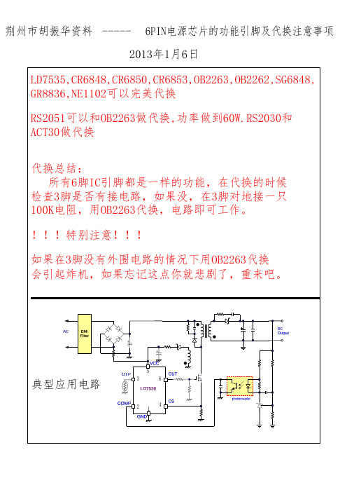
荆州市胡振华资料----- 6PIN电源芯片的功能引脚及代换注意事项2013年1月6日LD7535,CR6848,CR6850,CR6853,OB2263,OB2262,SG6848,GR8836,NE1102可以完美代换RS2051可以和OB2263做代换,功率做到60W.RS2030和ACT30做代换代换总结:所有6脚IC引脚都是一样的功能,在代换的时候检查3脚是否有接电路,如果没,在3脚对地接一只100K电阻,用OB2263代换,电路即可工作。
特别注意如果在3脚没有外围电路的情况下用OB2263代换会引起炸机,如果忘记这点你就悲剧了,重来吧。
典型应用电路53 6 2 1 44321TOP MARK YYWWPP567 8 pp231 65 4 YW P 36引脚功能DIP-8 (TOP VIEW)SOT-26 (TOP VIEW)OUTVCCCSGND COMP OTPPin DescriptionsPIN SOT-26 PIN DIP-8名称功能18GNDGround27COMPVoltage feedback pin (same as the COMP pin in UC384X). Connect a photo-coupler to close the control loop and achieve the regulation.35OTPPull this pin below 0.95V to shutdown the controller into latch mode until the ACresume power-on. Connecting this pin to ground with NTC will achieve OTP protection. Keep this pin float to disable the latch protection.4 4 CS Current sense pin, connect it to sense the MOSFET current5 2 VCC Supply voltage pin61OUTGate drive output to drive the external MOSFETO U TG N DC O M PN CV C CN CO T PC S芯片内部方框图Fig. 15Fig. 17A pull-high resistor is embedded internally and can be eliminated externally.A 230nS leading-edge blanking (LEB) time is included in the input of CS pin to prevent the false-trigger from the current spike. In the low power application, if the total pulse width of the turn-on spikes is less than 230nS and the negative spike on the CS pin below -0.3V, the R-C filter is free to eliminate. (As shown in Fig.16).However, the total pulse width of the turn-on spike is determined according to output power, circuit design and PCB layout. It is strongly recommended to adopt a smaller R-C filter (as shown in Fig. 17) for larger power application to avoid the CS pin being damaged by the negative turn-on spike.Output Stage and Maximum Duty-CycleAn output stage of a CMOS buffer, with typical 300mA driving capability, is incorporated to drive a power MOSFET directly. And the maximum duty-cycle of LD7536 is limited to 75% to avoid the transformer saturation.Voltage Feedback LoopThe voltage feedback signal is provided from the TL431 at the secondary side through the photo-coupler to the COMP pin of the LD7536. Similar to UC3842, the LD7536 would carry a diode voltage offset at the stage to feed the voltage divider at the ratio of RA and RB, that is,Fig. 16V -(PWM COMPARATOR ) =RBRA + RB⨯ (V COMP - V F )C5F1 3.15A/250V LL1 120uH L2 22mH330P/1206 R3R12.2MEG/1206R22.2MEG/1206NCX1 0.22uFBR1KBP206C4 82uF/400VR9 51K/1206 C6NC102pF/1206 R10T1ARM8C151R/1206D5 20120C7 470uF/25VC8470uF/25VC10 104P/080519V / 2.1A+VoR5620K/1206D1R6620K/120651k/1206R11 22R/1206D2 PR1007U1AR32DZ2/6.8VZENER1 RTNR40/0805 GS1002FLSMDR31330/08055.6k/0805T1BC11 4.7u/50VC12104P/08052 COMP5 VCCOUT 6R12B 10R/0805D6 D4148R12Q12SK3562IC432R251K/0805R29 4.3k/0805C16 R2862K/0805R30 /0805PC817B3.3nF/0805 LD7536CS 4200R/0805C13 3 OTPGNDR13100R/0805 C13 1 100P/0805C14100PF/0805R16A R16 1.4/1206 R16B 1.4/1206CY1 1.4/1206102P473p/0805 --- 40W (19V /2.1A )典型电源适配器电路图。
开关电源IC芯片

chiplink-semi南京芯联系列开关电源驱动芯片
AC/DC PSR:CL1132 、CL1128、CL1101、CL1100;PSR+MOS:CL1129、CL1112、CL1107、CL1103 ;PFC:CL6562; Flyback with MOSFET :CL1152;Flyback:CL1156、CL1160 、CL1158
AC/DC PWM Power Switch:SF1532、SF1533、SF1536、SF1537、SF1538、SF1539、SF1539HT、SF1548、SF1549、SF5582H、SF5582、SF5590;
原边反馈控制器/功率开关IC:SFL628、SFL629、SFL900、SF5920S、SF5920、SF5922、SF5922T、SF5922S、SF5922SV、SF5926SV、SF5926、SF5928SV、SF5928S、SF5928、SF6010L、SF6010F、SF6018、SF6040、SF6070、SF6072、SF6771、SF6772、SF6778、SF6781、SF6782、SF6788
Voltage Mode PWM Controller:AZ494A、AZ494C、AZ7500B、AZ7500C、AZ7500E、AZ7500F
Green Mode PWM Controller:AP3101、AP3102/AP3102V/AP3102L、AP3103、AP3105/AP3105V/AP3105L/AP3105R、AP3106、AP3105/AP3105H;AP3700、AP3700A、AP3700E、AP3710
液晶常用电源管理芯片

液晶常⽤电源管理芯⽚1200AP40 1200AP60、1203P60200D6、203D6 DAP8A 可互代203D6/1203P6 DAP8A2S0680 2S08803S0680 3S08805S0765 DP104、DP7048S0765C DP704加24V得稳压⼆极管ACT4060 ZA3020LV/MP1410/MP9141ACT4065 ZA3020/MP1580ACT4070 ZA3030/MP1583/MP1591MP1593/MP1430ACT6311 LT1937ACT6906 LTC3406/A T1366/MP2104AMC2576 LM2576AMC2596 LM2596AMC3100 LTC3406/AT1366/MP2104AMC34063A AMC34063AMC7660 AJC1564AP8012 VIPer12AAP8022 VIPer22ADAP02 可⽤SG5841 /SG6841代换DAP02ALSZ SG6841DAP02ALSZ SG6841DAP7A、DP8A 203D6、1203P6DH321、DL321 Q100、DM0265RDM0465R DM/CM0565RDM0465R/DM0565R ⽤cm0565r代换(取掉4脚得稳压⼆极管) DP104 5S0765 DP704 5S0765DP706 5S0765DP804 DP904FAN7601 LAF0001LD7552 可⽤SG6841代(改4脚电阻)LD7575PS 203D6改1脚100K电阻为24KOB2268CP OB2269CPOB2268CP SG6841改4脚100K电阻为2047KOCP1451 TL1451/BA9741/SP9741/AP200OCP2150 LTC3406/AT1366/MP2104OCP2160 LTC3407OCP2576 LM2576OCP3601 MB3800OCP5001 TL5001OMC2596 LM2596/AP1501PT1301 RJ9266PT4101 AJC1648/MP3202PT4102 LT1937/AJC1896/AP1522/RJ9271/MP1540SG5841SZ SG6841DZ/SG6841DSM9621 RJ9621/AJC1642SP1937 LT1937/AJC1896/AP1522/RJ9271/MP1540STRG5643D STRG5653D、STRG8653DTEA1507 TEA1533TEA1530 TEA1532对应引脚功能接⼊THX202H TFC719THX203H TFC718STOP246Y TOP247YV A7910 MAX1674/75 L6920 AJC1610VIPer12A VIPer22A[audio01]ICE2A165(1A/650V、31W);ICE2A265(2A/650V、52W);ICE2B0565(0、5A/650V、23W):ICE2B165(1A/650V、31W);ICE2B265(2A/650V、52W);ICE2A180(1A/800V、29W);ICE2A280(2A/800、50W)、KA5H0365R, KA5M0365R, KA5L0365R, KA5M0365RN# u) t! u1 W1 B) R, PKA5L0365RN, KA5H0380R, KA5M0380R, KA5L0380R1、KA5Q1265RF/RT(⼤⼩两种体积)、KA5Q0765、FSCQ1265RT、KACQ1265RF、FSCQ0765RT、FSCQ1565Q这就是⼀类得,这些型号得引脚功能全都⼀样,只就是输出功率不⼀样。
CR6853 电源IC规格书
3. 系统的启动时间:
上面两种启动方式当电源上电开机时通过启动电阻RIN 给VDD 端的电容C1 充电,直到VDD 端口电 压达到芯片的启动电压VTH(ON)(典型值14V)时芯片才被激活并且驱动整个电源系统正常工作。在图1.3.1
CR6853 电源管理 IC
深圳市振华凌云科技有限公司
中系统的最大启动延迟时间满足如下运算关系:
CR6853 电源管理 IC
深圳市振华凌云科技有限公司
产品设计应用指导书
Item No.: 产品编号: Product: 产品名称: Date: 日期:
CR6853 60W 电源管理控制 IC 2014/1/12
CR6853/CR6853B 应用指导书
摘要:
本文主要介绍了CR6853 的特征和详细的工作原理,描述了一种采用CR6853 的反激式隔离AC-DC 开 关电源的简单而高效的设计方法。CR6853B 为CR6853 的ESD 特别提高版本,功能和PIN 脚完全兼容。
CR6853 电源管理 IC
深圳市振华凌云科技有限公司
5. 正常工作频率和频率抖动
CR6853 允许设计者根据系统的使用环境需要自行调整系统的工作频率,其PWM 频率为:30-150K; CR6853 的典型工作频率为67KHz,其应用电路如图1.6,RI 的取值决定了系统的工作频率,工作频率的设 定可分别由以下公式计算出来,在正常的工作频率上增加了±4%的抖动,弱化在某个频率对外辐射的能量, 使系统设计更容易成功。
虽然CR6853 推荐系统PWM 的工作频率范围可为50K~150KHz,但是芯片系统性能优化主要是被设计 在 50KHz~67KHz 的应用范围, 在应用时请注意。 在PCB layout 时应尽可能使RI 的接地端靠近芯片的GND 端,以便减少干扰。
CR6848
符号
描述
VON VOFF VPROTECT ISTART IOPS
启动电压 关闭电压 保护电压 启动电流 工作电流
测试条件 IFB=0mA
最小值 15.1 10.1
典型值 16.1 11.1 26.7 20 1.46
最大值 16.6 12.1
单位 V V V uA mA
脉冲宽度调制参数
符号
描述
FPWM DPWM IFB_PFM
CR6848
图 14 斜坡补偿原理
功率限制
流经功率管的电流在 RSENCE 上产生一个电压 VSENCE,该电压直接控制 GATE 端的占空比,
同时就设定了变压器初级上的最大峰值电流
IMAX,根据变压器储存的能量
E
=
1 2
×
L × I MAX 2 ;
通过调节 RSENCE 的大小可以设定电源模块的最大输出功率;由于芯片内部存在系统延时 TD(从
功率变化,降低外围变压器和功率管损坏的可 能性。对于功率管翻转引入的开关噪声,通过 芯片内部集成的前沿消隐电路可以有效的滤 除,结合内部的过压保护和过流保护,大大地 提高电源模块的可靠性。另外,输出驱动的高 电平被钳位在 16.5V 以下,保证较高 VCC 时, 外部功率管不会因栅击穿而损坏;驱动死区时 间的引入减小了驱动时的贯通电流,而内部软 驱动电路则大大降低了功率管的开关噪声。
启达科技(成都)有限公司 V3.0
图 15 前沿消隐
成都启臣微电子有限公司 8/11
CR6848
过压保护
为了提高芯片的可靠性,延长芯片的寿命,CR6848 中集成了 26.7V 的过压保护电路,一旦 VCC 电压超过该值,输出 GATE 将会关闭。同时 VCC 电压迅速下降。
液晶电源IC的代换资料 2
格式如下好了"
液晶品牌与型号 电源管理芯片型号与封装 可代换型号
qBENQ 71G+ 1200AP40 直插 1200AP10 1200AP60
AOC 712SI EA1532A贴片
三星型号忘记 DM0565R
203D6 NCP1203D60R2 NCP1203D60R2G和DAP8A 直接代换
DAP02ALSZ与SG6841S可以互换
1200AP40和1200AP60直接代换
P5S0765和DP104、DP704直接代换
DP804和DP904直接代换
2S0680和2S0880直接代换
美格WB9D7575PS5
清华同方 XP911WD7575PS
联想LXM -WL19AH LXM-WL19BH D7575PS(早期有的用:NCP1203D6)
联想LXM-17CH:1203D6
方正17寸:1203D6与LD7575PS
方正19寸:LD7575PS
BenQ: FP94VW FP73G FP71G+S FP71G+G FP71GX等都是用:1200AP40
TEA1507和TEA1533直接代换
LD7535兼容 SG6848 (6849) / SG5701 / SG5848 /LD7535 (7550) / OB2262 (2263) / OB2278(2279)RS2051
LD7575和NCP1203、NCP1200 OB2268 SG5841 LD7552 OB2269 OB2268 RS20429
CR6850兼容SG6848/6849/5701/5848,OB2262/2263,LD7550/7535.
新款低成本绿色功率便携式PWM控制器CR6848说明书

CR6848Novel Low Cost Green-Power PWM Controller Featuresz Low Cost, PWM&PFM&CRMz Low Start-up Current (about 10µA)z Low Operating Current (about 2mA) z Current Mode Operationz Under Voltage Lockout (UVLO)z Built-in Synchronized SlopeCompensationz Programmable PWM Frequencyz Leading edge Blanking on Sense input z Constant output power limiting foruniversal AC inputz Cycle-by-cycle current limitingz Clamped gate output voltage 16.5Vz Over voltage protect 26.7Vz High-Voltage CMOS Process with ESD z SOT-23-6L、SOP-8 & DIP-8 Pb-Free Packagingz Compatible with SG5701 & SG5848 & LD7535 &OB22632/63Applicationsz Switching AC/DC Adaptor z Battery Charger z Open Frame Switching Power Supply z 384X ReplacementGeneral DescriptionThe CR6848 is a highly integrated low cost current mode PWM controller, which is ideal for small power current mode of offline AC-DC fly-back converter applications. Making use of external resistors, the IC changes the operating frequency and automatically enters the PFM/CRM under light-load/zero-load conditions. This can minimize standby power consumption and achieve green-power functions. With a very low start-up current, the CR6848 could use a large value start-up resistor (1.5Mohm). Built-in synchronized slope compensation enhances the stability of the system and avoids sub-harmonic oscillation. Dynamic peak limiting circuit minimizes output power change caused by delay time of the system over a universal AC input range. Leading edge blanking circuit on current sense input could remove the signal glitch due to snubber circuit diode reverse recovery and thus greatly reduces the external component count and system cost in the design. Pulse-by-pulse current limiting ensures safe operation even during short-circuit.The CR6848 offers more protection like OVP (Over Voltage Protection) and OCP (Over current protection). The CR6848’s output driver is clamped to maximum 16.5Vto protect the power MOSFET. Excellent EMI performance is achieved soft switching control at the totem pole gate driver output. CR6848 is offered in SOT-23-6, SOP-8 and DIP-8 packages.Dec, 2006 V1.5 1/14Block DiagramTYPICAL CHARACTERISTICSVDD startup Current VS TemperatureVDD (OFF) VS TemperatureOVP VS TemperatureDuty cycle VS TemperatureVDD startup Current VS TemperatureVDD Operation Current VS TemperaturePWM frequency VS TemperatureF OSC VS FB CurrentF OSC VS RI pin resistorDec, 2006 V1.5 8/14OPERATION DESCRIPTION Current ModelCompared to voltage model control, current model control has a current feedback loop. When the voltage of the sense resistor peak current of the primary winding reaches the internal setting value V TH , comparator reverse, register reset and power MOSFET cut-off. So that to detect and modulate the peak current cycle by cycle could control the output of the power supply. The current feedback has a good linear modulation rate and a fast input and output dynamic impact avoid the pole that the output filter inductance brings and the second class system descends to first class and so it widens the frequency range and optimizes overload protection and short circuit protection.Startup Current and Under Voltage LockoutThe startup current of CR6848 is set to be very low so that a large value startup resistor can therefore be used to minimize the power loss. For AC to DC adaptor with universal input range design, a 1.5 M Ω, 1/8 W startup resistor and a 10uF/25V VDD hold capacitor could be used.The turn-on and turn-off threshold of the CR6848 is designed to 16.1V/11.1V. During startup, the hold-up capacitor must be charge to 16.1V through the startup resistor. The hysteresis is implemented to prevent the shutdown from the voltage dip during startup.Internal Bias and OSC OperationA resistor connected between RI pin and GND pin set the internal constant current source to charge or discharge the internal fixed cap. The charge time and discharge time determine the internal clock speed and the switching frequency. Increasing the resistance will reduce the value of the input current and reduce the switching frequency. The relationship between RI pin and PWM switching frequency follows the below equation within the RI allowed range.)()(5800kHz K RI F OSC Ω=For example, a 100k Ω resistor RI could generate a 50uA constant current and a 58kHz PWM switching frequency. Thesuggested operating frequency range of CR6848 is within 48KHz to 100KHz.Green Power OperationThe power dissipation of switching mode power supply is very important in zero load or light load condition. The major dissipation result from conduction loss 、switching loss and consume of the control circuit. However, all of them related to the switching frequency. There are many difference topologies has been implemented in different chip. The basic operation theory of all these approaches intended to reduce the switching frequency under light-load or no-load condition.CR6848`s green power function adapts PWM 、PFM and CRM combining modulation. When RI resistor is 100k, the PWM frequency is 58kHz in medium or heavy load operation. Through modifying the pulse width, CR6848 could control output voltage. The current of FB pin increases when the load is in light condition and the internal mode controller enters PFM&PWM when the feedback current is over 0.92mA. The operation frequency of oscillator is to descend gradually. The invariable frequency of oscillator is 11.6kHz when the feedback current is over 1.05mA. To decrease the standby consumption of the power supply , Chip-Rail introduces the Cycle Reset Mode technology ;If the feedback current were over 1.1mA, mode controller of CR6848 would reset internal register all the time and cut off the gate pin, while the output voltage is lower than the set value, it would set register, gate pin operating again. Although the frequency of the internal OSC is invariable, the register would reset some pulses so that the practical frequency is decreased at the gate pin.CR6848 Green-Power FunctionDec, 2006 V1.5 9/14Internal Synchronized Slop Compensation Although there are more advantages of the current mode control than conventional voltage mode control, there are still several drawbacks of peak-sensing current-mode converter. Especially the open loop instability when it operates in higher than 50% of the duty-cycle. CR6848 is introduced an internal slope compensation adding voltage ramp to the current sense input voltage for PWM generation to solve this problem. It improves the close loop stability greatly at CCM, prevents the sub-harmonic oscillation and thus reduces the output ripple voltage.DUTYDUTY DUTYV MAXSLOP ×=×=4389.033.0Current Sensing & Dynamic peak limitingThe current flowing by the power MOSFET comes in to being a voltage V SENSE on the sense pin cycle by cycle, which compares to the internal reference voltage, controls the reverse of the internal register, limits the peak current IMAX of the primary of the transformer. The energy 221MAX I L E ××=deposited by the transformer. So adjusting the R SENSE can set the Max output power of the power supple mode. The current flowing by the power MOSFET has an extra valueD PINT L V I ×=∆ due to the system delay T that the current detected from the sense pin to power MOSFET cut off in the CR6848 (Among these, V IN is the primary winding voltage of the transformer and L P is theprimary wind inductance. IN V ranges from 85VAC to 264V AC. To guarantee the outputpower is a constant for universal input AC voltage, there is a dynamic peak limit circuit to compensate the system delay T that the system delay brings on.Leading-edge Blanking (LEB)Each time the power MOSFET is switched on, a turn-on spike will inevitably occur at the sense pin, which would disturb the internal signal from the sampling of the R SENSE . There is a 300n sec leading edge blanking time built in to avoid the effect of the turn-on spike and the power MOSFET cannot be switched off during this time. So that the conventional external RC filtering on sense input is no longer required.Over Voltage Protection (OVP)There is a 26.7V over-voltage protection circuit in the CR6848 to improve the credibility and extend the life of the chip. The GATE is to shutdown immediately when the voltage of the VDD is over 26.7V and the voltage of VDD is to descend rapidly.Gate Driver & Soft ClampedCR6848’ output designs a totem pole to drive a periphery power MOSFET. The dead time is introduced to minimize the transfixion current when the output is drove. The NMOS is shut off when the other NMOS is turned on. The clamp technology is introduced to protect the periphery power MOSFET from breaking down.。
LTC1163CS8#PBF;LTC1165CN8;LTC1165CN8#PBF;LTC1165CS8;LTC1165CS8#PBF;中文规格书,Datasheet资料

MOSFET DriversSFEATUREs Operates from 1.8V to 6Vs0.01µA Standby Currents95µA Operating Current per Channel at 3.3Vs Fully Enhances N-Channel Switchess No External Charge Pump Componentss Built-In Gate Voltage Clampss Easily Protected Against Supply Transientss Controlled Switching ON and OFF Timess Compatible with 5V, 3V and Sub-3V Logic Families s Available in 8-Pin SOIC D UESCRIPTIOThe LTC1163/LTC1165 triple low voltage MOSFET drivers make it possible to switch supply or ground referenced loads through inexpensive, low R DS(ON) N-channel switches from as little as a 1.8V supply. The LTC1165 has inverting inputs and makes it possible to directly replace P-channel MOSFET switches while maintaining system drive polar-ity. The LTC1163 has noninverting inputs. Micropower operation, with 0.01µA standby current and 95µA operating current, coupled with a power supply range of 1.8V to 6V, make the LTC1163/LTC1165 ideally suited for 2- to 4-cell battery-powered applications. The LTC1163/LTC1165 are also well suited for sub-3V, 3.3V and 5V nominal supply applications.The LTC1163/LTC1165 internal charge pumps boost the gate voltage 8V above a 3.3V rail, fully enhancing inexpen-sive N-channels for high- or low-side switch applications. The LTC1163/LTC1165 are available in both an 8-pin DIP and an 8-pin SOIC.SUPPLY VOLTAGE (V)GATEOUTPUTVOLTAGE(V)26810418LTC1163/65 • TA02426121416315MOSFET Switch Gate Voltage 2-Cell Triple High-Side SwitchU SA OPPLICATIs PCMCIA Card 3.3V/5V Switchs2-Cell High-Side Load Switchings Boost Regulator Shutdown to Zero Standby Currents Replacing P-Channel Switchess Notebook Computer Power Managements Palmtop Computer Power Managements Portable Medical Equipments Mixed 3.3V and 5V Supply SwitchingUA OPPLICATITYPICAL12LTC1163/LTC1165SYMBOL PARAMETER CONDITIONSMIN TYP MAXUNITS I QQuiescent Current OFFV S = 1.8V, V IN1 = V IN2 = V IN3 = V OFF (Note 1,2)0.011µA V S = 3.3V, V IN1 = V IN2 = V IN3 = V OFF (Note 1,2)0.011µA V S = 5V, V IN1 = V IN2 = V IN3 = V OFF (Note 1,2)0.011µA Quiescent Current ONV S = 1.8V, V IN = V ON (Note 2,3)60120µA V S = 3.3V, V IN = V ON (Note 2,3)95200µA V S = 5V, V IN = V ON (Note 2,3)180400µA V INH Input High Voltage 1.8V < V S < 2.7V q 80% × V S V 2.7V < V S < 6V q 70% × V SVV INL Input Low Voltage 1.8V < V S < 6V q 15% × V SV I IN Input Current 0V ≤ V IN ≤ V Sq±1µA C IN Input Capacitance 5pF V GATE – V SGate Voltage Above SupplyV S = 1.8V, V IN = V ON (Note 2)q 3.5 4.1 6.0V V S = 2V, V IN = V ON (Note 2)q 4.0 4.6 7.0V V S = 2.2V, V IN = V ON (Note 2)q 4.5 5.2 8.0V V S = 3.3V, V IN = V ON (Note 2)q 6.08.0 9.5V V S = 5V, V IN = V ON (Note 2)q5.09.013.0V t ONTurn-ON TimeV S = 3.3V, C GATE = 1000pF Time for V GATE > V S + 1V 40120400µs Time for V GATE > V S + 2V 60180600µs V S = 5V, C GATE = 1000pF Time for V GATE > V S + 1V 3095300µs Time for V GATE > V S + 2V40130400µsA UG WA WUW A R BSOLUTEXI TI SOperating Temperature RangeLTC1163C/LTC1165C........................... 0°C to 70°C Storage Temperature Range................ –65°C to 150°C Lead Temperature (Soldering, 10 sec)................. 300°CSupply Voltage ......................................................... 7V Any Input Voltage.......................... 7V to (GND – 0.3V)Any Output Voltage....................... 20V to (GND – 0.3V)Current (Any Pin)................................................. 50mAWUUPACKAGE/ORDER I FOR ATIOV S = 1.8V to 6V, T A = 25°C, unless otherwise noted.ELECTRICAL C C HARA TERISTICSLTC1163C/LTC1165C /3LTC1163/LTC1165ELECTRICAL C C HARA TERISTICSV S = 1.8V to 6V, T A = 25°C, unless otherwise noted.SYMBOL PARAMETER CONDITIONSMIN TYP MAX UNITSt OFFTurn-OFF TimeV S = 3.3V, C GATE = 1000pFTime for V GATE < 0.5V 2065200µs V S = 5V, C GATE = 1000pF Time for V GATE < 0.5V1545150µsLTC1163C/LTC1165C The q denotes specifications which apply over the full operating temperature range.Note 1: Quiescent current OFF is for all channels in OFF condition.Note 2: LTC1163: V OFF = 0V, V ON = V S . LTC1165: V OFF = V S , V ON = 0V Note 3: Quiescent current ON is per driver and is measured independently.Gate Voltage Above SupplySupply Current per Driver ONStandby Supply CurrentC C HARA TERISTICSU WA TYPICAL PERFOR CE SUPPLY VOLTAGE (V)0SU P P L Y C U R R E N T (µA )5 4 3 2 1 0 –11234LTC1163/65 • TPC0156SUPPLY VOLTAGE (V)V G A T E – V S (V )1210 8 6 4 2 01234LTC1163/65 • TPC0356SUPPLY VOLTAGE (V)0S U PP L Y C U R R E N T (µA )600 500 400 300 200 100 01234LTC1163/65 • TPC0256Input Threshold VoltageTurn-ON TimeTurn-OFF TimeSUPPLY VOLTAGE (V)0I N P U T T H R E S H O L DV O L T A G E (V )65 4 3 2 1 01234LTC1163/65 • T PC0456SUPPLY VOLTAGE (V)T U R N -O N T IM E (µs )600500 400 300 200 100 01234LTC1163/65 • TPC0556SUPPLY VOLTAGE (V)0T U R N -OF F T I M E (µs )300250 200 150 100 50 01234LTC1163/65 • TA06564LTC1163/LTC1165C C HARA TERISTICSU WA TYPICAL PERFOR CE PI FU CTIO SU U U Input PinsThe LTC1163 is noninverting; i.e., the MOSFET gate is driven above the supply when the input pin is held high.The LTC1165 is inverting and drives the MOSFET gate high when the input pin is held low. The inverting inputs of the LTC1165 allow P-channel switches to be replaced by lower resistance/cost N-channel switches while maintain-ing system drive polarity.The LTC1163/LTC1165 logic inputs are high impedance CMOS gates with ESD protection diodes to ground and therefore should not be forced below ground. The inputs can however, be driven above the power supply rail as there are no clamping diodes connected between the input pins and supply pin. This facilitates operation in mixed 5V/3V systems.Output PinsThe output pin is either driven to ground when the switch is turned OFF or driven above the supply rail when the switch is turned ON. The output is clamped to about 14V above ground by a built-in Zener clamp. This pin has a relatively high impedance when driven above the rail (the equivalent of a few hundred k Ω). Care should be taken to minimize any loading of this pin by parasitic resistance to ground or supply.Supply PinA 150Ω resistor should be inserted in series with the ground pin or supply pin if negative supply voltage tran-sients are anticipated. This will limit the current flowing from the power source into the LTC1163/LTC1165 to tens of milliamps during reverse battery conditions.OPERATIOUThe LTC1163/LTC1165 are triple micropower MOSFET drivers designed for operation over the 1.8V to 6V supply range and include the following functional blocks:3V Logic Compatible InputsThe LTC1163/LTC1165 inputs have been designed to accommodate a wide range of 3V and 5V logic families.The input threshold voltage is set at roughly 50% of the supply voltage and approximately 200mV of input hyster-esis is provided to ensure clean switching.The input enables all of the following circuit blocks: the bias generator, the high frequency oscillator and gate charge pump. Therefore, when the input is turned off, the entire circuit powers down and the supply current drops below 1µA.Standby Supply CurrentTEMPERATURE (°C)0S U P P L Y C U R R E N T (µA )5 4 3 2 1 0 –110203040LTC1163/65 • TPC07506070MOSFET Gate Drive CurrentGATE VOLTAGE ABOVE SUPPLY (V)1G A T E D R I V E C U R R E N T (µA )1010010004680.1210LTC1163/65 • TPC09Supply Current per Driver ONTEMPERATURE (°C)0S U P P L Y C U R R E N T (µA )300 250200150 100 50 010203040LTC1163/65 • TPC08506070/5LTC1163/LTC1165OPERATIOUGate Charge PumpGate drive for the power MOSFET is produced by an internal charge pump circuit which generates a gate volt-age substantially higher than the power supply voltage.The charge pump capacitors are included on chip and therefore no external components are required to generate gate drive.Controlled Gate Rise and Fall TimesWhen the input is switched ON and OFF, the gate is charged by the internal charge pump and discharged in a controlled manner. The charge and discharge rates have been set to minimize RFI and EMI emissions.BLOCK DIAGRA W(One Channel)APPLICATIO S I FOR ATIOW UU U Logic-Level MOSFET SwitchesThe LTC1163/LTC1165 are designed to operate with logic-level N-channel MOSFET switches. Although there is some variation among manufacturers, logic-level MOSFET switches are typically rated with V GS = 4V with a maximum continuous V GS rating of ±10V. R DS(ON) and maximum V DS ratings are similar to standard MOSFETs and there is generally little price differential. Logic-level MOSFETs are frequently designated by an “L” and are usually available in surface mount packaging. Some logic-level MOSFETs are rated with V GS up to ±15V and can be used in applications which require operation over the entire 1.8V to 6V range.Powering Large Capacitive LoadsElectrical subsystems in portable battery-powered equip-ment are typically bypassed with large filter capacitors to reduce supply transients and supply induced glitching. If not properly powered however, these capacitors may themselves become the source of supply glitching.For example, if a 100µF capacitor is powered through a switch with a slew rate of 0.1V/µs, the current during start-up is:I START = C(∆V/∆t)= (100 × 10–6)(1 × 10⁵)= 10AObviously, this is too much current for the regulator (or output capacitor) to supply and the output will glitch by as much as a few volts.The startup current can be substantially reduced by limit-ing the slew rate at the gate of an N-channel as shown in Figure 1. The gate drive output of the LTC1163/LTC1165is passed through a simple RC network, R1 and C1, which substantially slows the slew rate of the MOSFET gate to approximately 1.5 × 10⁻⁴V/µs. Since the MOSFET is operating as a source follower, the slew rate at the source is essentially the same as that at the gate, reducing the startup current to approximately 15mA which is easilyGATEINPUT6LTC1163/LTC1165APPLICATIO S I FOR ATIOW UU U Figure 1. Powering a Large Capacitive Loadon a 3.3V supply which is compatible with 5V TTL and CMOS logic. (The LTC1163/LTC1165 cannot however, be driven by 3V logic when powered from a 5V supply because the threshold is approximately 2.5V.)TYPICAL APPLICATIO SUPCMCIA Card 3.3V/5V V CC SwitchNOTE: USE LTC1163 WITH NONINVERTING PCMCIA CONTROLLERSmanaged by the system regulator. R2 is required to eliminate the possibility of parasitic MOSFET oscillations during switch transitions. It is a good practice to isolate the gates of paralleled MOSFETs with 1k resistors to decrease the possibility of interaction between switches.Mixed 5V/3V SystemsBecause the input ESD protection diodes are referenced to ground instead of the supply pin, it is possible to drive the LTC1163/LTC1165 inputs from 5V CMOS or TTL logic even though the LTC1163/LTC1165 are powered from a 3.3V supply as shown in Figure 2. The input threshold voltage is approximately 50% of the supply voltage or 1.6VReverse Battery ProtectionThe LTC1163/LTC1165 can be protected against reverse battery conditions by connecting a 150Ω resistor in series with the ground pin or supply pin. The resistor limits the supply current to less than 24mA with –3.6V applied.Because the LTC1163/LTC1165 draw very little currentwhile in normal operation, the drop across the resistor is minimal. The 3.3V µP (or control logic) can be protected by adding 10k resistors in series with the input pins.Figure 2. Direct Interface to 5V LogicV IN/7LTC1163/LTC1165Information furnished by Linear Technology Corporation is believed to be accurate and reliable.However, no responsibility is assumed for its use. Linear Technology Corporation makes no represen-tation that the interconnection of its circuits as described herein will not infringe on existing patent rights.TYPICAL APPLICATIO SU2-Cell to 3.3V, 5V and 12V High-Side Switch/Converterwith 0.01µA Standby Current3.3VµF3.3VUltra-Low Drop Triple 3.3V High-Side SwitchPCMCIA Card Socket V PP Switch/ReglatorV CC MMDF3N02HDPP = 0V, 3.3V,EN0 0 1 0 1EN1 0 0 1 1OUTPUT 0V 12V V CC HI-Z8LTC1163/LTC1165Linear Technology Corporation1630 McCarthy Blvd., Milpitas, CA 95035-7487(408) 432-1900 qFAX : (408) 434-0507 qTELEX : 499-3977© U SA OPPLICATITYPICAL S8 Package 8-Lead Plastic SOICPACKAGE DESCRIPTIO U3-Cell to 3.3V Ultra-Low Drop Regulator with 2 Ramped SwitchesµFMixed Voltage High- and Low-Side SwitchesN8 Package 8-Lead Plastic DIPDimensions in inches (millimeters) unless otherwise noted.–0.3818.2550.053 – 0.069 BSC/分销商库存信息:LINEAR-TECHNOLOGYLTC1163CS8#PBF LTC1165CN8LTC1165CN8#PBF LTC1165CS8LTC1165CS8#PBF LTC1163CS8LTC1165CS8#TR LTC1165CS8#TRPBF LTC1163CS8#TR LTC1163CS8#TRPBF LTC1163CN8LTC1163CN8#PBF。
- 1、下载文档前请自行甄别文档内容的完整性,平台不提供额外的编辑、内容补充、找答案等附加服务。
- 2、"仅部分预览"的文档,不可在线预览部分如存在完整性等问题,可反馈申请退款(可完整预览的文档不适用该条件!)。
- 3、如文档侵犯您的权益,请联系客服反馈,我们会尽快为您处理(人工客服工作时间:9:00-18:30)。
CR6848 电源管理 IC
深圳市振华凌云科技有限公司
CR6848 电源管理 IC
深圳市振华凌云科技有限公司
前沿消隐(LEB)
开关管的每次开启不可避免带来开关毛刺,它可以通过RSENCE 采样后,对内部信号进行干 扰,对RS 触发器发出错误的清“0”信号。为了消除开关毛刺的影响,CR6848 中集成了300nS 的前沿消隐电路。该电路可以有效的滤除RSENCE 上的毛刺,减小RS 触发器的误动作;在干扰 较大的应用场合,外接一个小的RC 滤波电路可以达到更好的效果。
偏置电流&振荡器
偏置电流由内部的基准电压和外部的RI 端电阻决定。当RI 电阻采用100K 欧姆时,偏置 电流为48uA,该电流通过对内部电容的充电和放电形成RC 振荡,减小RI 的阻值可以增加振 荡器的工作频率,反之减小振荡器的工作频率;充电电流和放电电流的比例由内部固定,振荡 器的最大占空比是一个固定值:PWM 工作时为75%,PFM 稳定时为25%;振荡器的工作频率 由下式给出:
特点
� � � � � � � � � � � � 低电流模PWM控制 低启动电流 低工作电流 极少的外围元件 片内自带前沿消隐 (300nS) 额定输出功率限制 UVLO欠压锁定 (12.1V~16.1V) 内建同步斜坡补偿 PWM工作频率可调 输出电压钳位 (16.5V) PWM&PFM相结合 周期电流限制
应用(小于60W)
CR6848 电源管理 IC
深圳市振华凌云科技有限公司
CR6848 电源管理 IC
深圳市振华凌云科技有限公司
电气特性(Ta=25°C
(除了另作说明),
VDD = 16V)
CR6848 电源管理 IC
深圳市振华凌云科技有限公司
CR6848 电源管理 IC
深圳市振华凌云科技有限公司
CR6848 电源管理 IC
深圳市振华凌云科技有限公司
过压保护
为了提高芯片的可靠性,延长芯片的寿命,CR6848 中集成了26.7V 的过压保护电路,一旦 VCC 电压超过该值,输出GATE 将会关闭。同时VCC 电压迅速下降。
Hale Waihona Puke 输出驱动CR6848 输出采用图腾柱结构驱动外围一个大的功率MOS 管;为了减小驱动时的贯通电流, 引入了死区时间,如图:当一个NMOS 关断后,另外一个NMOS 才开启;同时,为了保护外 围的功率管不会发生栅击穿和钳位齐纳管的电流饱和,在输出上采用了软钳位技术。
CR6848 电源管理 IC
深圳市振华凌云科技有限公司
� � � � � � � � � � � �
软驱动 2500V的ESD保护 过载保护 过压保护(26.7V) 高压BiCMOS工艺 SOT-23-6L和DIP-8L 无铅封装 AC/DC电源适配器 电池充电器 开放式电源 备用开关电源 机顶盒开关电源 384X 代替
欠压锁定&启动电流
CR6848 的欠压锁定设定在11.1V 到16.1V 之间;上电开始,桥式整流后的电源通过启动电 阻对VCC 端电容充电,当VCC 电压大于16.1V 时,欠压锁定模块发出使能信号(高),芯片开 始工作;当VCC 端电压低于11.1V,欠压锁定下拉使能,芯片停止工作。为了减小启动电阻上 的 功 率 损 耗 , 芯 片 内 部 集 成 了 200K 欧 的 电 阻 , 启 动 电 流 小 于 20uA ; 静 态 电 流 小 于 2mA 。
CR6848 电源管理 IC
深圳市振华凌云科技有限公司
电流模控制
电流控制比电压控制多了一个电流反馈环节。当初级线圈上的峰值电流在采样电阻RSENCE 上的幅度达到内部设定值VTH 时,比较器翻转,锁存器复位,功率管截止。这样逐个检测和调节电 流脉冲就可以达到控制电源输出的目的。电流反馈具有良好的线性调整率和快速的输入输出动 态响应;消除了输出滤波电感带来的极点,使系统由二阶降为一阶,频响特性好,稳定幅度大。
CR6848 电源管理 IC
深圳市振华凌云科技有限公司
斜坡补偿
如果没有斜坡补偿且占空比大于50 %,整个控制环路变得不稳定,抗干扰性能差。CR6848中, 将RSENCE采样回来的电压信号和内部的斜坡补偿信号相加,然后与光藕反馈回来的误差信号比较 来控制Gate的占空比,达到稳定输出的目的。在每一个开关循环里面引入一个同步的斜坡补偿 可以提高系统的稳定性,防止电压毛刺产生的次谐波振荡。但是,过大的斜坡补偿会影响电路 的正常工作,所以CR6848中:
CR6848 电源管理 IC
深圳市振华凌云科技有限公司
产品设计应用指导书
Item No.: 产品编号: Product: 产品名称: Date: 日期:
CR6848 5-6W 电源管理控制 IC 2014/1/12
CR6848 推荐 5-6W 应用,兼容 OB2535、CR6235、RM3261
概述