芯片ISL6752的原理和应用
开关电源小论文

1.开关电源研究的背景及意义现实生活中常用的电源,可以分为发出电能的电源和变换电能的电源两大类。
我们把输人和输出都是电能的电源称之为变换电能的电源。
开关电源就是属于变换电能的电源,此种电源就是电路中的电力电子器件工作在开关状态的电源。
开关电源的前身是线性稳压电源。
在我们生活中,大多数电子装置、电气控制设备的工作电源是直流电源。
在开关电源出现之前,这些装置的工作电源都采用线性稳压电源。
在20世纪50年代,美国宇航局以小型化、重量轻为目标,为搭载火箭而开发了开关电源。
在半个多世纪的电力电子技术发展历程中,开关电源因具有体积小、重量轻、效率高、发热量低、性能稳定等优点而逐渐取代传统技术制造的相控稳压电源,并广泛应用于电子整机设备中。
在现代社会,电子信息设备与人们的生活、工作的关系越来越密切,而所有的电子设备都离不开电源。
高速发展的计算机技术带领人类进入了信息社会,同时也促进了电源技术的迅速发展。
电源技术的精髓是电能变换,即利用电能变换技术,将市电或电池等一次电源变换成适用于各种用电对象的二次电源。
开关电源技术属于电力电子技术,它运用功率变换器进行电能变换。
经过变换的电能,可以满足各种用电需求。
由于其高效节能可带来巨大经济效益,因而引起社会各方面的重视而得到迅速推广。
2.国内外研究现状及发展趋势开关电源真正的发展是从70年代开始的,在此期间系统的电力电子理论的确立。
电力电子理论为开关电源的发展提供了一个良好而必需的基础。
但在产品应用的初期,存在开关频率低(20kHz以下)、功率密度比较低、可靠性较差的缺点。
因此开关电源主要的发展方向,是针对上述缺点不断加以改善。
大功率场效应管(MOSFET)及绝缘栅晶体管(IGBT)等器材的出现为高频和大功率变换器提供了极有利的条件。
新的器件和新的拓扑理论的出现使得开关电源技术日趋可靠、成熟、经济、适用。
开关电源目前的发展,主要朝着更高的功能密度和变换效率及更好的动态特性;更好的环保性能;智能化与高可靠性;更广泛的应用等方向发展。
中文ISL6752

ISL6752输出时序图 输出时序图
状态一: 、 导通 导通, 、 关断 关断。 状态一:UL、LR导通,LL、UR关断。
t1时刻,励磁电感Lm 在Vin 之下开始励磁。
im (t ) = Vin (t − t1 ) + im (t1 ) Lm
LL D4 C4 Ls LR D3 C3 Vin D1 C1 D2 C2
ห้องสมุดไป่ตู้
UL
UR
在t1时刻,励磁电感Lm中 的励磁电流 im(t1)=-Im。 输出电感Lo的端电压在t1时 刻也随之跳变(见上图所 示),其状态也由之前的 能量释放状态转为存储能 量状态。
Is(t)
Io(t)
D5
+
Lo
Co Ro
+
Lm
Np
-
Ns1
Im(t)
+
Ip(t)
+
Ns2 D6
状态二: 关断 关断,UR、LL仍关断,UL仍开通。 状态二:LR关断
t2时刻,LR关断,C2开始 放电和C3开始充电。因原 边绕组电流Ip(t)近似于恒 定,故C2、C3的是线性充 放电,到了t21时刻,电容 C2 的电压UC2从VIN下降到 UOxNP/NS。 。 其中: 其中:
I ⋅ (t − t 2 ) U C 2 (t ) = Vin − C 2 C2
Vin
Vin D1 C1 D2 C2 UL UR
LL
D4
C4
Ls
LR
D3
C3
Is(t)
Io(t)
D5
Lo
+
Co Ro
Ns1 Lm Np
Im(t)
Ns2 D6
Ip(t)
ISL6752(6754)EVAL1Z ZVS DC Power Supply with Synchronous Rectifiers User Guide
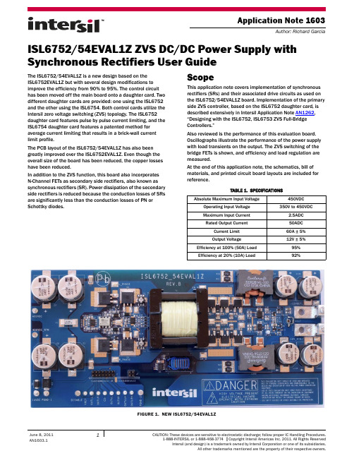
Application Note 1603Author: Richard GarciaISL6752/54EVAL1Z ZVS DC/DC Power Supply with Synchronous Rectifiers User GuideThe ISL6752/54EVAL1Z is a new design based on the ISL6752EVAL1Z but with several design modifications to improve the efficiency from 90% to 95%. The control circuit has been moved off the main board onto a daughter card. Two different daughter cards are provided: one using the ISL6752 and the other using the ISL6754. Both control cards utilize the Intersil zero voltage switching (ZVS) topology. The ISL6752 daughter card features pulse by pulse current limiting, and the ISL6754 daughter card features a patented method for average current limiting that results in a brick-wall current limit profile.The PCB layout of the ISL6752/54EVAL1Z has also been greatly improved over the ISL6752EVAL1Z. Even though the overall size of the board has been reduced, the copper losses have been reduced.In addition to the ZVS function, this board also incorporates N-Channel FETs as secondary side rectifiers, also known as synchronous rectifiers (SR). Power dissipation of the secondary side rectifiers is reduced because the conduction losses of SRs are significantly less than the conduction losses of PN or Schottky diodes.ScopeThis application note covers implementation of synchronous rectifiers (SRs) and their associated drive circuits as used on the ISL6752/54EVAL1Z board. Implementation of the primary side ZVS controller, based on the ISL6752 daughter card, is described extensively in Intersil Application Note AN1262, “Designing with the ISL6752, ISL6753 ZVS Full-Bridge Controllers.”Also reviewed is the performance of this evaluation board. Oscillographs illustrate the performance of the power supply with load transients on the output. The ZVS switching of the bridge FETs is shown, and efficiency and load regulation are measured.At the end of this application note, the schematics, bill of materials, and printed circuit board layouts are included for reference.TABLE 1.SPECIFICATIONSAbsolute Maximum Input Voltage450VDCOperating Input Voltage 350V to 450VDCMaximum Input Current 2.5ADC Rated Output Current50ADC Current Limit 60A ± 5%Output Voltage12V ± 5%Efficiency at 100% (50A) Load 95%Efficiency at 20% (10A) Load92%FIGURE 1.NEW ISL6752/54EVAL1ZBlock DiagramThe evaluation board is composed of several distinct circuit elements. The three main sections are the ZVS full bridge on the input, the current doubler rectifier on the output, and the controller daughter card. See “Schematics- Main Board,ISL6752/54EVAL1Z” on page23 and “Schematics - Daughter Card” on page25 for complete circuit details.Daughter CardsThe ISL6752 or ISL6754 control ICs are located on their respective daughter cards, as shown in Figures 3 and 4. Both daughter cards have the control ICs on the primary side and the voltage error amplifier on the secondary side. Creepage spacing between the primary and secondary is maintained on the cards. The ISL6752 and the ISL6754 control ICs are located on the primary side, eliminating the need for two AC line isolating gate drive transformers to drive the primary side bridge FETs. Instead, the low side FETs are driven directly by MOSFET drivers (on the main board), and the high side FETs are driven by a gate drive transformer that only requires operational insulation. Primary side control also simplifies design of the current sensing transformers because they also do not have to be AC line isolating.A line isolation rated opto-coupler (D5 on ISL6752DB or D2 on ISL6754DB) passes the analog error signal generated by the error amplifier, U1, from the secondary to the primary. Opto D3 passes a digital signal from primary to secondary to turn off the SRS for diode emulation. The only functional difference between the ISL6752 andISL6754 daughter cards is how current limit is implemented. The ISL6752 uses pulse-by-pulse current limit, and the ISL6754 uses average current limit.Special test points located on the daughter cards aid in probing nodes on the daughter cards for evaluation. Test points PGND and TP_PRI are located on the primary side, and SGND andTP_SEC are located on the secondary. With these test points, the user can employ the spring-like probe accessories included withFIGURE 2.ISL6752/54EVAL1Z BLOCK DIAGRAMFIGURE 3.ISL6752 DAUGHTER CARDmany scope probes. The scope signal pin is inserted in TP_PRI (or TP_SEC), and the short spring ground lead is inserted in PGND (or SGND).To probe any node on the daughter card, solder a 30ga insulated wire between the desired node and the via that is associated with the TP_PRI or TP_SEC test point. This method not only simplifies probing of any node, but also implements the preferredtechnique of measuring small signals in the presence of high amplitude switching magnetic fields.The ISL6752DBEVAL1Z and the ISL6754DBEVAL1Z daughter cards are also available as standalone evaluation kits.ZVS Full BridgeThe low side FETs, Q 3 and Q 4, are driven directly by the ISL89160 MOSFET driver, U1 (Figure 5). The two high-side FETs, Q 1 and Q 2, are indirectly driven by the ISL89160 driver, U2. A level translating gate drive transformer, T 3, with complementary output windings, directly drives the high-side bridge FETs with a symmetrical square wave. The design of T 3 is simplified because it only needs 400V operational insulation, and it is always driven with a square wave, thus eliminating the problems associated with non-symmetrical drive waveforms.Observe that the ISL89160 MOSFET drivers are located as close as possible to their respective bridge FETs to minimize thedetrimental effects of parasitic inductance on the outputs of the drivers. Although the input signal lead lengths between the drivers and the daughter card are relatively long (about 5cm), they are shielded on top and bottom by ground planes, to significantly reduce the noise injected on these lines. Thehysteresis of the ISL89160 inputs also lessens the possibility of noise corrupting the gate signals.High Voltage ProtectionBecause a failure of the bridge can cause catastrophic damage to the primary side control elements, a voltage crowbar, F1 and D 3, and a voltage blocking diode, D 4, are incorporated (Figure 6). D 3 clamps the bias voltage to a safe level. If 400V is applied to the V DD node, F1 opens shortly after D3 conducts current. D 4provides additional protection by blocking high voltage from being applied to the 13V lab supply. Note that a fully debugged power supply does not need these additional components. These parts are included on the evaluation board to minimize damage, should the user accidently introduce a fault while evaluating thecircuits. The designer may want to keep F1 in the final design, toprevent a loud bang if the bridge does fail.FIGURE 4.ISL6754 DAUGHTER CARDFIGURE 5.FULL BRIDGEFIGURE 6.PROTECTION CIRCUITSPrimary Side Current SensingThe primary side bridge has two current sensing transformers, T 2 and T 4, one on each leg on the drains of the low-side bridge FETs (Figure 7). Using two transformers allows each CT to reset during alternate half cycles. Alternate current sensing methods are reviewed in “Current Sensing” on page 8.Synchronous Rectifier Drive CircuitTwo banks of SRs are driven by the ISL89163 MOSFET driver, U4 (Figure 8). An RCD network on the inputs to this driver delay the turn-on of the SRs relative to the turn-off of the primary side bridge FETs.The ISL89367, U108, can optionally be used to drive the SRs instead of the ISL89163. Review “Schematics - Daughter Card” on page 25 to understand how to disconnect the ISL89163 and connect the ISL89367.The pulse transformer, T 6, crosses the isolation boundary to couple the control signals from the ISL6752, ISL6754 to the MOSFET drivers (Figure 9). Note that this transformer alsoprovides the secondary side bias voltage for the MOSFET drivers.Current Doubler OutputThe current doubler output is composed of two banks of SRs, Q 107... Q 109 and Q 111... Q 113; inductors L 102and L 103; and output filter capacitors, C 133... C 136 (Figure 10). The advantage of this topology is that the output current is shared by the two inductors, thus reducing conduction losses. Another advantage isthat the secondary winding of the power transformer does not require a center tap.FIGURE 7.PRIMARY SIDE CURRENT SENSINGFIGURE 8.SRs AND DRIVERSFIGURE 9.PULSE TRANSFORMER AND DRIVERBasic SR PrinciplesReplacing diodes with MOSFETs has two major advantages:•Dramatically reduces conduction losses•The applied duty cycle remains virtually constant from no load to full load. Disadvantages are:•Additional complexity and cost•Higher reverse recovery losses as compared to fast recovery diodes.•When paralleling units for redundancy, provisions must be made to prevent current circulation among the paralleled units.SR Drive Timing RequirementsTo emulate a diode, an SR must be driven ON when a diode would normally be conducting. But unlike a diode, if the SR is ON, the current through the SR can reverse if the voltage on the SR “cathode” becomes positive. The consequence is that if the SR is driven ON when the primary side is sourcing voltage to the secondary, the secondary side will be shorted by the SR. Figure 11 illustrates the timing required to drive the SRs. Notethat the rising edges of the two lower bridge FETs are delayed bythe ISL6752/54 relative to the PWM signal. Likewise, the risingedges of the SRs gate signals are delayed by the ISL89163relative to the falling edge of the PWM signal. These delays arenecessary to prevent the overlap of drive signals that wouldresult with high amplitude short circuit currents.When an SR is turned off while current is flowing from source todrain, the current diverts from the FET channel to the internalbody diode. Because the voltage drop across the body diode ishigher than the channel, it is desirable to minimize dissipation byminimizing the duration of the current flow through the bodydiode.FIGURE 10.CURRENT DOUBLER OUTPUTFIGURE 11.TIMING FOR SRs AND BRIDGE FETsSR Drive and BiasOUTLLN and OUTLRN in Figure 12 are control signals from the ISL6752/54 that are used to drive the SRs. Because theISL6752/54 is located on the primary side, a pulse transformer, T6, is used to cross the isolation boundary. The simplified schematic of Figure 12 illustrates the use of T6 to not only couple OUTLLN and OUTLRN to the secondary, but also to generate the bias for drivers on the secondary.When /OUTLLN or /OUTLRN (outputs of EL7212) transitions to a logic high, it is necessary to turn off the associated SR quickly. For example, when /OUTLRN (blue) transitions high, V1 is high, and C10 is quickly discharged by Q100. U4 then drives R-SR off. In a similar manner, when /OUTLLN is high, U4 drives L-SR off. When /OUTLLN or /OUTLRN transitions to a logic low, it is necessary to turn on the SRs after a time delay, to prevent the SRs from shorting the primary side bridge when it is sourcing current. For example, when /OUTLRN transitions to low, V1 is low and Q100 turns off, allowing C10 to be charged by R27. When the positive threshold of UR is exceeded, the output of U4 drives on R_SR. In a similar manner, the high to low transition of/OUTLLN results in the output of U4 driving on L_SR after a time delay.Note that the cathodes of D9 are connected together to peak charge C123. Because C123 is large in value, after the initial charging, the voltage does not change significantly from cycle to cycle. An important aspect of generating the bias for U4 in this manner is that the thresholds for the logic transitions on the inputs of U4 are proportional to VBIAS, and the voltage to charge C9 and C10 is also VBIAS. Consequently, the delays generated by the RC networks are independent of the absolute value of VBIAS. Current DoublerFigure 13 illustrates the current flow in the two inductors of the current doubler topology. Current flow in the circuit is correlated with the waveforms by color coding. The green waveform represents the sum of red and blue currents through R LOAD. For circuit clarity, paralleled SRs and output capacitors of theISL6752/54EVAL1Z board are not shown.When using diodes (instead of SRs), if the average load current is less than half of the ramp current in the output inductors, the current in the inductors becomes discontinuous, and the duty cycle of the PWM is shortened to maintain the desired output voltage. When using SRs, the inductor currents in L1 and L2 can become negative because current in SRs can flow bidirectionally; consequently, the duty cycle remains virtually unchanged. The benefit is that the load transient performance is the same for any load from zero up to current limit. Another advantage is that, for very light loads, the duty cycle is not reduced to very small duty cycles, pulse skipping does not occur, and the associated voltage jitter does not happen.An important design consideration for the current doubler topology is that the DC resistance of both halves must be equal. PCB layout must be as symmetrical as possible, and the DCRs of the inductors should be reasonably equal. If not, the current between the two sides does not split equally. Because perfect physical PCB symmetry is not always possible, current sharing between inductors must be confirmed.In Figure 14, inductor current waveforms are taken from the ISL6752/54EVAL1Z board. Current balance between the two inductors was achieved after one board revision. The inductor currents maintain the same waveform shape even at no load. Another design consideration when using SRs is how to connect the outputs of multiple power supplies in parallel for redundancy or increased power capacity. A consequence of negative current flow in an SR (when a diode would otherwise be reverse biased and off) is that power can be transferred from the secondary to the primary if one of the paralleled outputs has a higher voltage. The voltage loop of the units with lower set point voltages attempts to pull down the voltage by sinking current from the higher set point units. The primary side bridge capacitor is charged by the secondary side, eventually resulting in excessive voltage damage. This damage can be avoided by using OR-ing diodes (or FETs) on the paralleled outputs. Another solution is to turn off the SRs (diode emulation mode) when the current reverses in the SRs, but this eliminates some of the advantages of using SRs. Paralleling features are not implemented on the ISL6752/54EVAL1Z board.FIGURE 13.CURRENT FLOW IN TWO INDUCTORS OF CURRENT DOUBLER TOPOLOGYFIGURE 14.INDUCTOR CURRENT WAVEFORMS 50A LOAD30A LOAD NO LOADCurrent SensingCurrent flowing from the secondary to the primary can result in an unanticipated malfunction of the current sensing transformer circuit if reverse SR currents are not considered. Figure 15 shows a commonly used primary side current sensing circuit utilizing one current sensing transformer (CT).This circuit works well for peak current mode control if power is always flowing from primary to secondary, as is the case when diodes are used instead of SRs. Figure 16 illustrates the performance of the current sensing output when power always flows from primary to secondary.The voltage across R S is as expected. The vertical dashed lines show when the power cycle is terminated at the required peak of the current.Figure 17 illustrates what happens at no load to the sense voltage across R S.Notice that the negative components of the primary transformer current are rectified, resulting in two peaks of current across R S for each half cycle. Under steady state conditions, the rectified negative component may cause erratic performance because the cycle can terminate on the first peak (the inverted peak, as indicated by the vertical red line) instead of the required second peak. This condition can easily be corrected by having a small load across the output to ensure that the negative peak is always less than the positive.A minimum load, however, does not correct a more serious problem that occurs when there is a large load step from a heavy load to no load. When the load current is interrupted, the output capacitor charges higher than the regulated voltage. As the regulation loop is starting to respond by slewing to a minimum duty cycle, the excessive voltage on the output capacitor starts to discharge back to the primary. This results in a large negative current at the beginning of the duty cycle, which causes the duty cycle to be terminated very early. The imbalance of the applied volt-seconds to the power transformer may saturate the power transformer and damage the power bridge.Another scenario is that the current sensing transformer itself may saturate, which also damages the bridge. The control loop cannot maintain balanced alternate half cycles applied to the power transformer without valid current sense information. There are three solutions to this problem. Figure 18 illustrates the placements of two current sensing transformers, one on each drain leg of the bottom FETs.In this configuration, only positive current flowing into the drains of the bottom FETs are sensed across R S, solving the problem of rectified negative currents being impressed across R S. An advantage of using two CTs is that there is a full half cycle available to reset the cores of the CTs. This is the solution used in the ISL6752/54EVAL1Z board.FIGURE 15.PRIMARY SIDE CURRENT SENSING CIRCUIT UTILIZINGONE CTFIGURE 16.PERFORMANCE OF CURRENT SENSING OUTPUTFIGURE 17.NO LOAD SENSE VOLTAGE ACROSS R SFigure 19 shows a different current sensing implementation that also solves the problem shown in Figure 15. In this example, both drain currents of the bottom FETs are sensed by only one CT. There are some limitations that must be considered, however. The minimum time available to reset the core is the duration of the selected dead time between the two FETs on the same side of the bridge. To accommodate the resetting of the CT, this dead time can be made longer, but the consequences of reducing the maximum duty cycle available for output voltage regulation mustIf the dead time is kept short, then the peak voltage required for resetting the core is relatively large. For example, assume that the selected dead time is 2% of the duty cycle. The resultingworst-case reset voltage is shown approximately in Equation1:In Equation 1, V SMAX is 1V (the current limit voltage of theISL6752); this is the ideal reset voltage. In practice, however, the parasitic capacitance of the output windings suppresses the peak voltage, and consequently, the reset time increases. If a custom current sensing transformer is designed, the effects of the parasitic capacitance can be minimized by increasing the space between turns. If a standard, off-the-shelf transformer is used, however, the output capacitance may be too large to allow long duty cycles. In this case, the two-transformer solution may be necessary.Notice in Figure 19 that the 400V RTN is slightly more negative than signal ground. This configuration is recommended for applications that directly drive the bottom FETs with MOSFET drivers. If the 400V RTN and the MOSFET drivers are grounded, regenerative feedback will be present on the output of the MOSFET drivers because of the CT windings in the gate drive loop.A variation on the current sense circuit in Figure 19 is to place the current sensing transformer in the common drain lead of the two high-side FETs, as shown in Figure 20.The circuits shown in Figures 19 and 20 give exactly the same performance, but the problem associated with the gate drives (as explained in Figure 19) is avoided. The disadvantage of placing the CT at this location is that the CT must be designed with400VDC operational insulation.ConclusionThis application note reviews the use of MOSFETs as synchronous rectifiers to replace conventional diodes. The advantages of improved power efficiency and load transient are reviewed along with implementation problems that must be solved.The use of daughter cards for the ISL6752 and ISL6754 control ICs also allows comparison of cycle-by-cycle peak current limiting and average current limiting.TRANSFORMERSFIGURE 19.CURRENT SENSING TRANSFORMER IN THE COMMON SOURCE LEAD0.980.02⁄()V SMAX49V=•(EQ. 1)FIGURE 20.DRAIN LEADReferences[1]Fred Greenfeld, Intersil Application Note AN1246,“Techniques to Improve ZVS Full-bridge Performance”[2]Fred Greenfeld, Intersil Application Note AN1262, “Designingwith the ISL6752, ISL6753 ZVS Full-bridge Controllers”[3]Richard Garcia, Intersil Application Note AN1619, “Designingwith ISL6752DBEVAL1Z and ISL6754DBEVAL1Z ControlCards”Evaluation Board Set-upThe following sections cover the set-up of theISL6752/54EVAL1Z evaluation board. Also included are waveforms, performance parameters, PCB layout, and schematics.Setting UpLab Equipment Required•DC bias power supply, 12.6VDC @ 200mA minimum •Adjustable 0VDC-400VDC regulated lab power supply, 2.5ADC minimum with current limit•Fan to cool heatsinks•Oscilloscope, digital preferred, with 4 channels, 20MHz minimum bandwidth•Adjustable DC load (electronic or resistor), 70A @ 12V,100A @ 0V min, >850W•DC Multimeter•Infra-red temperature probe (optional but highly recommended)Turn-On Procedure1.Solder a wire between DISABLE and PGND-1 lugs located onthe lower left side of the main board. Optionally connect a switch between these two lugs.2.Install either of the daughter control cards onto the mainboard.3.Connect the DC load to the outputs of the evaluation board.Adjust the load to zero current.4.With both supplies turned off, connect the DC bias supply tothe +13V terminal and PGND.5.Connect the 400V supply to +400V and 400V RTN.6.Turn on the DC bias supply and adjust the current limit to200mA. Adjust the voltage to +12.6 VDC. The lab supplycurrent should be approximately 150mA.7.Turn on the 400V supply and adjust the current limit to 2.5A.Adjust the voltage to 400VDC. Do not exceed 450VDC. The current should be approximately 45mA.8.Turn on the fan and direct the air flow through the heatsinksmounted on the bottom of the board.ing the test points that are adjacent to the output powerlugs, measure the output voltage of 12V ±0.5VDC.The output load and input voltage can now be safely adjusted. Because there is no thermal shut-down circuit, it is important to maintain adequate airflow over the heatsinks, especially when applying large loads. It is recommended to measure the temperature of the power FETs (primary bridge and secondary SRs) to ensure that their temperatures do not exceed +85°C. It is usually necessary to have only a moderate airflow over the heatsinks, even under worst-case loads.Danger•This evaluation unit should be used and operated only by persons experienced and knowledgeable in the design and operation of high voltage power conversion equipment. •Use of this evaluation unit constitutes acceptance of all risk inherent in the operation of equipment having accessible hazardous voltage. Careless operation may result in serious injury or death.•Use safety glasses or other suitable eye protection.•A line isolated 400VDC supply is required. CautionA voltage clamp, D3, is used to protect the primary side control circuit from catastrophic damage should the high voltage bridge fail. In order to prevent this clamp from conducting, do not adjust the bias supply above 13.5VDC.WaveformsZVSIn Figure 21, the drain-source voltage of the low-side FETs relative to the gate voltage is displayed to highlight the ZVS performance of the bridge. The load is at the rated 50A. Notice that full ZVS is not achieved because the minimum resonance voltage is about 25VDC. Also, the gate drive is turning on late (about 25ns), allowing the resonant voltage to start rising. Eventhough the optimum zero voltage switching is not achieved, 98% of the switching losses are still recovered [(4002-502)/4002=98%]. This improvement over the ISL6752EVALZ was achieved by increasing the leakage inductance of thetransformer and by using bridge FETs with less body capacitance.In Figure 22, resonant switching with 50% load still saves 84% of the switching losses. Other techniques can be used to improve ZVS performance. For more information, see Application NoteAN1246, “Techniques to Improve ZVS Ful-bridge Performance”.ZVS WaveformsFIGURE 21.RESONANT SWITCHING WITH 100% (50A) LOADFIGURE 22.RESONANT SWITCHING WITH 50% (25A) LOADLoad Transients WaveformsFIGURE 23.STEP LOAD: 0A TO 12.5A (12.5A DELTA)FIGURE 24.STEP LOAD: 25A TO 37.5A (12.5A DELTA)FIGURE 25.STEP LOAD: 37.5A TO 50AFIGURE 26.STEP LOAD: 0A TO 25AFIGURE 27.STEP LOAD: 0A TO 50AFIGURE 28.SHORT CIRCUIT RELEASE WITH ISL6754V OUT recovers after a short circuit is removed when using the ISL6754DBEVAL controller.After the short is removed, V OUT increases linearly because the output capacitance is being charged with a constant current (~55A).NOTE:Output Ripple and Noise WaveformsFIGURE 29.OUTPUT RIPPLE, 50A LOAD, 40MHz BANDWIDTHFIGURE 30.OUTPUT RIPPLE, 50A LOAD, 145MHz BANDWIDTHTransformer Current, Primary Winding WaveformsFIGURE 31.PRIMARY TRANSFORMER CURRENT vs OUTPUT LOAD TRANSIENT (25A TO 50A)FIGURE 32.PRIMARY TRANSFORMER CURRENT vs OUTPUT LOAD TRANSIENT (50A TO 25A)Performance CurvesFIGURE 33.POWER EFFICIENCY vs LOAD (ISL6752 OR ISL6754)FIGURE 34.LOAD REGULATION FIGURE 35.PULSE BY PULSE vs AVERAGE CURRENT LIMIT21015202570758085909295100OUTPUT CURRENT (A)E F F I C I E N C Y (%)6560555030354045505592% EFFICIENCY WITH 20% LOAD12.0011.9511.9011.8511.80ISL6754ISL6752102030405060I OUT (A)V O U T (V )01020304050607080I OUT (A)V O U T (V )121086420ISL6754ISL6752Application Note 1603Bill of MaterialsPART NUMBERQTY UNITS REFERENCE DESIGNATORDESCRIPTION MANUFACTURER MANUFACTURER PART ISL6752/54EVAL1ZREVBPCB1eaPWB-PCB,ISL6752_54EVAL1Z, REV B, ROHSIMAGINEERING INCISL6752/54EVAL1ZREVBPC BC3216X7R1C475K-T 2eaC11, C17CAPACITOR, SMD, 1206, 4.7µF, 16V, 10%, X7R, ROHSTDK C3216X7R1C475KC4532X7R2J104K-T 2ea C5, C18CAP, SMD, 1812, 0.1µF, 630V, 10%, X7R, ROHSTDKC4532X7R2J104K GA355QR7GF332KW01L-T 2ea C20, C121CAP, SMD, 2220, 3300pF, 250V, 10%, X7R, ROHSMURATA GA355QR7GF332KW01L H1046-00102-100V10-T 2ea C14, C15CAP, SMD, 0805, 1000pF, 100V, 10%, X7R, ROHSVENKEL C0805X7R101-102KNE H1046-00102-50V5-T 2ea C9, C10CAP, SMD, 0805, 1000pF, 50V, 5%, NP0, ROHS PANASONIC ECU-V1H102JCX H1046-00105-25V10-T 5ea C6, C12, C13, C16, C22CAP, SMD, 0805, 1.0µF, 25V, 10%, X5R, ROHS AVX 08053C105KAT2A H1065-00106-25V10-T 1ea C123, C132CAP, SMD, 1206, 10µF, 25V, 10%, X5R, ROHS VENKEL C1206X5R250-106KNE H1082-00475-50V10-T 4ea C7, C8, C127, C129CAP, SMD, 1210, 4.7µF, 50V, 10%, X7R, ROHS MURATA GRM32ER71H475KA88L SER2814L-332KL2eaL102, L103COIL-PWR INDUCTOR, SMD, 3.3µH, 10%, 48A, 1.2m Ω, ROHS COILCRAFTSER2814L-332KLUUG1C222MNL1ZD 4ea C133-C136CAP, SMD, 16X16.5, 2200µF, 16V, 20%, AL.EL., ROHS NICHICON UUG1C222MNL1ZDUUG2W330MNL1MS 4ea C1-C4CAP, SMD, 18X21.5, 33µF, 450V, 20%, ALUM.ELEC, ROHS NICHICON UUG2W330MNL1MS131-4353-001ea VOUT CONN-SCOPE PROBE TEST PT, COMPACT, PCBMNT, ROHSTEKTRONIX 131-4353-001514-26eaa) 13VDC, 400VDC, PGND-1, PGND-2, DISABLE CONN-TURRET, TERMINAL POST, TH, ROHSKEYSTONE 1514-21514-20ea b) 400VDC_RTNCONN-TURRET, TERMINAL POST, TH, ROHSKEYSTONE 1514-250029ea a) CS+, VREF, OUTLL, OUTLR, OUTUL, OUTUR CONN-MINI TEST POINT, VERTICAL, WHITE, ROHS KEYSTONE500250020ea b) SR_EN, OUTLLN, OUTLRNCONN-MINI TEST POINT, VERTICAL, WHITE, ROHSKEYSTONE 50025016-T13eaa) GLL, GLR, LLN, LRN, SR_A, SR_B, PGND-3, 2, +12VOUT, 12V RTN CONN-COMPACT TEST POINT, SMD, ROHS KEYSTONE50165016-T 0ea b) SGND-1, SGND-CONN-COMPACT TEST POINT, SMD, ROHSKEYSTONE 50165016-Teac) L_PHASE, R_PHASE CONN-COMPACT TESTPOINT, SMD, ROHSKEYSTONE5016。
ISL6752_06中文资料

Pinout
ISL6752 (QSOP) TOP VIEW
VADJ 1 VREF 2 VERR 3 CTBUF 4 RTD 5 RESDEL 6 CT 7 CS 8 16 VDD 15 OUTLL 14 OUTLR 13 OUTUL 12 OUTUR 11 OUTLLN 10 OUTLRN 9 GND
FN9181.2 April 4, 2006
OVERTEMPERATURE PROTECTION
OUTLL OUTLR OUTLLN OUTLRN
VADJ
ISL6752
OSCILLATOR + 1.00V 70ns LEADING EDGE BLANKING 80mV + PWM COMPARATOR 0.33 VREF 1mA CS
3
400 VDC VIN-
R12 + Vout Q12 Q10A R1 Q10B C10 Q9A Q9B Q13 C12 L1 C15 C7
+
R13 RETURN
Q6A Q4 Q6B
Q7A Q7B
Q3
C13
ISL6752
R18
R17 R19 T2 CR1 R8 R2 R20 VADJ VREF VERR CTBUF RTD RESDEL R3 CT CS R4 Q11 R23 R24 Q14 U3 U2 R22 R21 R5 R6 C16 C6 R14 R7 U1 R24 VDD OUTLL OUTLR OUTUL OUTUR OUTLLN OUTLRN GND C11 R15 CR4 U5 U4 EL7212 C5 T4 R23 EL7212 C14
R19
FN9181.2 April 4, 2006
数字电源优势分析

开关电源技术是电力电子技术的一个重要领域,有着广阔应用前景,近年来,随着DSP 等电子器件的小型化、高速化,开关电源的控制部分正在向数字化方向发展。
用于开关电源的数字控制器已经在电力电子领域中引起了越来越多的关注,各种在模拟电路中难以实现的现代控制方法也开始应用于开关电源的控制中,大大丰富了开关电源的控制方案。
数字控制系统的概述信号处理实际就是构造信号与信号之间的传递函数,实现方法有两种:模拟方式和数字方式。
模拟方式使用电容、电阻、运算放大器等模拟器件来直接实现滤波、补偿、比较等控制功能,而数字方式则是先将模拟量数字化,再进行数字处理,然后还原成模拟信号。
(a)模拟控制开关变换器(b)数字控制开关变换器图a、b为模拟控制开关变换器与数字控制开关变换器的结构图。
两者相同的部分为功率单元和滤波单元,不同部分在于控制单元:模拟控制开关变换器采用模拟控制器,包括模拟补偿网络、脉冲宽度调制器(PWM)和斜坡信号;而数字控制开关变换器采用数字控制器,包括模数转换器(A/D Converter)、数字补偿器(Compensator)和数字脉冲宽度调制器(DPWM)。
模拟控制系统是传统的电路控制形式,经过多年研究,技术已经非常成熟。
随着电力电子技术及其控制技术的不断发展,模拟控制的局限性也越来越明显。
首先,模拟元器件的元器件老化问题和不可补偿的温漂问题,以及受环境干扰(如工作环境温度,电磁噪声等)等因素都会影响控制系统的长期稳定性。
同时,模拟控制系统需要大量的分立元件和电路板,器件数量多,制造成本高,对于每一个采用模拟控制的电路装置,其控制系统都需要专门的设计。
每一次产品的更新换代,都需要重新设计、制作它们的控制系统。
另外,目前大多数的模拟控制回路,仍采用传统的PID调节,而很少采用现代控制理论提供的控制方案。
在高性能低价格的微控制器和DSP处理器不断涌现的今天,数字控制系统的应用越来越广。
因为与传统的模拟控制器相比,基于DSP的数字控制器具有如下优点:●系统构成简单和可靠性高与模拟控制相比,完成同一任务,数字信号处理器的外围电路简单,数字控制器使用非常少的模拟元器件,解决了模拟控制中元器件老化和温漂带来的问题。
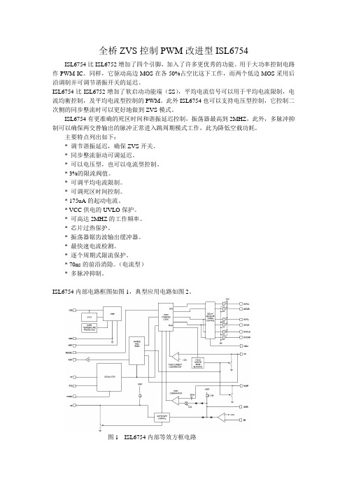
PWM控制技术的最新科技成果-介绍ISL6752

PWM控制技术的最新科技成果-----全桥零电压开关次级零电压同步整流的控制IC-ISL6752ISL6752是英赛尔公司05年最新的科技成果。
它不用移相技术就获得了初级侧的软开关拓扑,同时克服了全桥移相电路不能确保次级ZVS同步整流的毛病。
第一次做到了初,次级同时实现ZVS开关,从而实现了功率MOSFET在开关电源中的最佳工作状态。
ISL6752是一个高性能,可供选择的少引脚数ZVS全桥PWM控制器。
与英赛尔公司的ISL6551相比,它获得的ZVS工作是通过驱动上边桥MOSFET在一个固定的50%的占空比,下边桥MOSFET在跟随沿被谐振开关延迟调制的方法。
和我们熟悉的移相控制方法相比,这个方法提供了同等的效率,但是用简单的少引脚封装的IC,它还改进了过流保护和轻载时的性能。
ISL6752的特点是为了实现同步整流控制,PWM互补输出用一个外部控制电压,这个互补输出与相关的PWM输出可以在相位上动态的超前或者滞后。
这个最先进BICMOS设计特点使振荡频率可以调节到2MHz,有可调节的软启动,精确的死区时间调节和谐振延迟控制。
除此以外,多脉冲抑制确保了交替输出脉冲在低占空比可能发生的脉冲跳跃问题。
它的方框电路如图1。
图1 ISL6752控制IC 内部等效方框电路引脚说明:VDD IC的供电端子,为了免除噪声干扰加一个陶瓷旁路电容。
RTD这是振荡器定时电容放电电流控制端,接一个电阻到GND。
流过该电阻的电流决定了放电电流的大小,放电电流通常为20X该电流。
PWM的死区时间取决于定时电容的放电脉宽。
在RTD端的电压通常是2V。
CT振荡器定时电容端子,并连接到GND。
它通过内部200μΑ电流源充电,并通过可以调节的TRD控制端放电。
V ADJ用一个0-5V的电压加到此输入端来实现相位的延迟和超前。
(OUTLL与OUTLLN之间,OUTLR与OUTLRN之间)。
而OUTUL与OUTUR之间OUTUR与OUTLR之间的相位关系仍然保持,而不管OUTLL与OUTLR, OUTLLN与OUTLRN之间的相位关系。
基于Mathcad的高效率全桥DC-DC控制部分的设计

基于Mathcad的⾼效率全桥DC-DC控制部分的设计
基于Mathcad的⾼效率全桥DC-DC控制部分的设计
李臻;康龙云
【期刊名称】《新型⼯业化》
【年(卷),期】2016(006)012
【摘要】本⽂针对采⽤了先进的全桥软开关电流模式PWM控制芯⽚ISL6752控制的全桥DC-DC拓扑,使⽤Mathcad设计计算软件,简化了全桥拓扑关键控制参数的设计过程.本⽂先介绍了系统整体结构,设置了主电路的基本参数.然后,把从控制到输出的控制环路分为了三级,并分别推导了它们的等效数学模型.最后,为了验证设计的有效性,本⽂使⽤Mathcad搭建了控制系统三级组成的数学模型,并绘制了整个系统的伯德图.通过反复调试控制补偿电路参数,得到了满意的系统频率响应特性,验证了对采⽤
ISL6752芯⽚的全桥拓扑控制部分建模以及设计的准确性.
【总页数】6页(9-14)
【关键词】全桥DC-DC;ISL6752;Mathcad
【作者】李臻;康龙云
【作者单位】华南理⼯⼤学电⼒学院,⼴东⼴州510640;华南理⼯⼤学电⼒学院,⼴东⼴州 510640
【正⽂语种】中⽂
【中图分类】
【相关⽂献】
1.基于Intersil全桥ZVS控制器的⾼效率DC-DC变换器设计 [J],
2.⾼效率倍流与同步整流之⾮对称半桥DC-DC转换器设计与实现[C], 吴黎明;。
ZVS全桥控制IC-ISL6754
全桥ZVS控制PWM改进型ISL6754ISL6754比ISL6752增加了四个引脚,加入了许多更优秀的功能。
用于大功率控制电路作PWM-IC。
同样,它驱动高边MOS在各50%占空比这下工作,而两个低边MOS采用后沿调制并可调节谐振开关的延迟。
ISL6754比ISL6752增加了软启动功能端(SS),平均电流信号可以用于平均电流限制,电流均衡控制,及平均电流型控制的PWM。
此外ISL6754也可以支持电压型控制,它控制二次侧的同步整流时可以更好地做到ZVS模式。
ISL6754有更准确的死区时间和谐振延迟控制,振荡器最高到2MHZ,此外,多脉冲抑制可以确保两交替输出的脉冲正常进入跳周期模式工作,此为降低空载功耗。
主要特点列出如下:* 调节谐振延迟,确保ZVS开关。
* 同步整流驱动可调延迟。
* 可以电压型,也可以电流型控制。
* 3%的限流阀值。
* 可调平均电流限制。
* 可调死区时间控制。
* 175uA的起动电流。
* VCC供电的UVLO保护。
* 可高达2MHZ的工作频率。
* 芯片过热保护。
* 振荡器锯齿波输出缓冲器。
* 最快速电流检测。
* 逐个周期式限流保护。
* 70ns的前沿消隐。
(电流型)* 多脉冲抑制。
ISL6754内部电路框图如图1,典型应用电路如图2。
图1 ISL6754内部等效方框电路图2 ISL6754基本应用电路各引脚功能如下:*VDD---IC供电端,加旁路电容到GND。
用瓷介电容紧靠VDD和GND。
*GND---IC公共端,信号地,功率地采用一个端子。
由于在高峰值电流及高频工作台,必须要一个低阻抗布局接地线尽量短。
*VREF---5V基准电压端。
有3%的偏差。
要用0.1---2.2uF的瓷电容旁路。
*CT---振荡器定时电容端。
外接于此端到GND,由内部200uA电流源充电,放电速率由RTD电阻决定。
*RTD---振荡器定时电容放电电阻,接于此端到地。
决定CT电流放电幅度,最小为20*电阻电流。
- 1、下载文档前请自行甄别文档内容的完整性,平台不提供额外的编辑、内容补充、找答案等附加服务。
- 2、"仅部分预览"的文档,不可在线预览部分如存在完整性等问题,可反馈申请退款(可完整预览的文档不适用该条件!)。
- 3、如文档侵犯您的权益,请联系客服反馈,我们会尽快为您处理(人工客服工作时间:9:00-18:30)。
1-888-INTERSIL or 1-888-468-3774 | Intersil (and design) is a registered trademark of Intersil Americas Inc.
Copyright Intersil Americas Inc. 2005, 2006, 2008. All Rights Reserved
3
ISL6752
VIN+
+ C1
400 VDC
CR2
Q8A R10 Q8B Q1
C8
R1
VIN-
Q6A Q4 Q6B
T3
CR3
R11 Q5A Q2
Q5B C9
Q10A C10
Q9A
Q10B
Q9B
Q7A Q3 Q7B
T1
R13 C13
T2 CR1
R2 R3
Q11
VDD C2
VR1
R19 R8
R20
R7 R4
R1
VREF R7
R8 R9
R6
VADJ VREF
VDD OUTLL
ISL6752
VERR OUTLR
CTBUF OUTUL
RTD
OUTUR
RESDEL OUTLLN
CT
OUTLRN
CS
GND
U1
SECONDARY BIAS
SUPPLY
C2
R4
R5
C6
R2 R3
C3 C4 C5
T1 Np:Ns:Ns = 9:2:2
®
Data Sheet
October 31, 2008
ISL6752
FN9181.3
ZVS Full-Bridge Current-Mode PWM with Adjustable Synchronous Rectifier Control
The ISL6752 is a high-performance, low-pin-count alternative zero-voltage switching (ZVS) full-bridge PWM controller. Like Intersil’s ISL6551, it achieves ZVS operation by driving the upper bridge FETs at a fixed 50% duty cycle while the lower bridge FETs are trailing-edge modulated with adjustable resonant switching delays. Compared to the more familiar phase-shifted control method, this algorithm offers equivalent efficiency and improved overcurrent and light-load performance with less complexity in a lower pin count package.
4
ISL6752
VIN+
Q1 Q5 R13 CR2
T3 1:1:1
Q2 Q6 CR3 R12
400 VDC
+ C1
Q4 Q7A R10
Q7B
CR4 C8
Q10A
C10
Q10B
T4 1:1:1
Q9A Q9B
CR5
Q3 Q8A R11 Q8B C9
Q11A
C7
Q12A
Q11B
Q12B
VIN-
T2 CR1
Thermal Information
Thermal Resistance Junction to Ambient (Typical)
Operating Conditions
Temperature Range . . . . . . . . . . . . . . . . . . . . . . . . .-40°C to +105°C Supply Voltage Range (Typical). . . . . . . . . . . . . . . . 9VDC to 16VDC
Ns
Np
Ns
Q16
R14 Q15
C11
R15 L1
C12
C13 C14 +
Q13A Q13B
Q14A Q14B
R17
C16
C17
Q17
C15 R18
R16
R20
VREF R22
U3 +
R19 R21
C18
+ VOUT RETURN
FN9181.3
October 31, 2008
ISL6752
Absolute Maximum Ratings (Note 2)
ISL6752 (16 LD QSOP) VREF 2 VERR 3 CTBUF 4
RTD 5 RESDEL 6
CT 7 CS 8
16 VDD 15 OUTLL 14 OUTLR 13 OUTUL 12 OUTUR 11 OUTLLN 10 OUTLRN 9 GND
1
CAUTION: These devices are sensitive to electrostatic discharge; follow proper IC Handling Procedures.
Features
• Adjustable Resonant Delay for ZVS Operation • Synchronous Rectifier Control Outputs with Adjustable
Delay/Advance • Current-Mode Control • 3% Current Limit Threshold • Adjustable Deadtime Control • 175µA Start-up Current • Supply UVLO • Adjustable Oscillator Frequency Up to 2MHz • Internal Over-Temperature Protection • Buffered Oscillator Sawtooth Output • Fast Current Sense to Output Delay • Adjustable Cycle-by-Cycle Peak Current Limit • 70ns Leading Edge Blanking • Multi-Pulse Suppression • Pb-Free (RoHS Compliant)
R5 R6
C3 C17 C4 R21
VADJ
VDD
VREF OUTLL
ISL6752
VERR OUTLR
CTBUF OUTUL
RTD
OUTUR
RESDEL OUTLLN
CT
OUTLRN
CS
GND
U1
R23
R24
R22
C16
EL7212 C5 T4
U5
R23 CR4
Q14 C6
R24 U2
Q12 Q13
Supply Voltage, VDD . . . . . . . . . . . . . . . . . . . GND - 0.3V to +20.0V OUTxxx . . . . . . . . . . . . . . . . . . . . . . . . . . . . . . . GND - 0.3V to VDD Signal Pins . . . . . . . . . . . . . . . . . . . . . . . GND - 0.3V to VREF + 0.3V VREF . . . . . . . . . . . . . . . . . . . . . . . . . . . . . . . . . GND - 0.3V to 6.0V Peak GATE Current . . . . . . . . . . . . . . . . . . . . . . . . . . . . . . . . . . 0.1A
70ns LEADING
EDGE BLANKING
+
-
PWM COMPARATOR
80mV 0.33
VREF 1mA
CS VERR
ISL6752
Typical Application - High Voltage Input Primary Side Control ZVS Full-Bridge Converter
The ISL6752 features complemented PWM outputs for synchronous rectifier (SR) control. The complemented outputs may be dynamically advanced or delayed relative to the PWM outputs using an external control voltage.
EL7212 U4
R12 C12
L1 C15
C7 +
+ VOUT
RETURN
R18 R17
R16
C14
C11 R15
U3 R14
FN9181.3
October 31, 2008
Typical Application - High Voltage Input Secondary Side Control ZVS Full-Bridge Converter