psim_opampsim运放仿真
运放的仿真与分析报告

运放的仿真与分析1.基本仿真流程(1)电路仿真界面:进入UNIX系统,按键“Ctrl+t”出现下图窗口:图1输入“icfb&”回车后出现下图窗口。
图2注:有关镜像的操作:图2中选择“Library Path Editor”出现下图窗口:图3左栏为文件名,右栏为路径;或者打开文件cds.lib 按下图编写文件图4图5File→New→Library(opam)→(New)Cell View进入电路图编辑界面,画相应的放大器电路,如下图图6(2)调用相关器件器件的调用操作:按快捷键“i”,选择library,以及相应的器件(nmos,pmos,res,cap等)注:模型名要与模型库中的相应名称相同。
打开模型库的.scs文件,查看模型名和器件的基本参数(,,t V ):ox th// Models included in this release ://// Model Name Description// ----------- ----------------------------------------------------------------------// nmos_1p8 BSIM3v3 model for thin-gate (1.8V) NMOS transistor// pmos_1p8 BSIM3v3 model for thin-gate (1.8V) PMOS transistor// nmos_3p3 BSIM3v3 model for thick-gate (3.3V) NMOS transistor// pmos_3p3 BSIM3v3 model for thick-gate (3.3V) PMOS transistor// nmos_1p8_nat BSIM3v3 model for thin-gate (1.8V) Native NMOS transistor// nmos_3p3_nat BSIM3v3 model for thick-gate (3.3V) Native NMOS transistorsection nmos_1p8_tmodel nmos_1p8 bsim3v3 {0: type=n+ lmin=1.8e-007 lmax=3.5e-007 wmin=2.2e-007………………………………………………………….+ xw=0 tox=3.5e-009 toxm=3.5e-009…………………………………………………+ xpart=0 vth0=0.39851301 lvth0=1.1573677e-008…………………………………………………..+ cdscd=0 cit=0.0017786 u0=0.035597185………………………………….//***************************************************************************** section pmos_1p8_tmodel pmos_1p8 bsim3v3 { 0: type=p+ lmin=1.8e-007 lmax=3.5e-007 wmin=2.2e-007………………………………………………….+ xl=0 xw=0 tox=3.5554e-009…………………………………………….+ cgdo=3.051e-010 xpart=0 vth0=-0.39889023…………………………………………..+ u0=0.0078211697 lu0=1.2538533e-010 wu0=5.1065658e-010…………..…………………………….注:在sim.scs 文件中没有表示沟道调制效应的参数λ,因而需要测量计算: 修正后的漏电流为 2()(1)D n GS T DS i K v V v λ=-+图7如图可求出λ。
PSIM仿真

作用:测量电路的电压和电流,并把它们传到控制电路。
自动化与信工程学院电气系
--电子线路CAD--Байду номын сангаас
2、探头和仪表
作用:来测量电压,电流,功率和其他值。
连接方式:串或并其中。
自动化与信工程学院电气系
--电子线路CAD--
控制部分
开关控制器 传递函数 计算模块 逻辑元器件
数字控制模块
PISM的开关模型是理想化的,导通或者关断瞬间 可以忽略的。开关导通时电阻10 μΩ ,而关断为1MΩ。 开关不需缓冲电路。
自动化与信工程学院电气系
--电子线路CAD--
•单开关管
二极管
晶闸管
可关断晶闸管
BJT
MOSFET
IGBT
双向开关
自动化与信工程学院电气系
--电子线路CAD--
4 检测单元
作用:连接门极控制信号和功率开关。输入是来自控 制电路的逻辑信号,并传到功率电路作为门信号。
On-off switch controllers are used as the
interface between control gating signals and
power switches.
The input, which is a logic signal (either 0
3、α控制器
作用:控制晶闸管开关或桥的延迟角。 控制器有3 个输入: α 值:移相α 角度延迟 同步信号:同步信号从低到高的转变(0 到1),提供了同步, 并且与延迟角α 等于0 的时刻相一致。 使能信号:使能输出。
自动化与信工程学院电气系
--电子线路CAD--
相关元器件
psim与simulink联合仿真步骤

psim与simulink联合仿真步骤(1) 在 PSIM 安装目录下,运行程序文件“SetsimPath.exe”,将“SimCoupler Module”以 S 函数的形式嵌入 MATLAB/Simulink,以实现两种软件之间的数据交换,达到联合仿真的目的。
(或者直接在打开的psim菜单“utilities”中点击“SimCoupler setup”)(2) 在 PSIM 中搭建主电路仿真模型,并在 Elements/Control/SimCoupler 下拉菜单中,分别用 In Link Node 和 Out Link Node 与主电路仿真模型的输入输出变量相连。
并使用 Simulate/Arrange Slink Nodes 菜单项排列各 In/Out Link Nodes 的顺序,以便Simulink 环境下的 SimCouplerBlock按相同的顺序显示各输入输出端口。
Simulate/generate netlist file菜单项来产生网络表,并保存在同一目录下。
在 Simulink 环境下从工具包窗口中的 S-function SimCoupler 菜单下放置一个 SimCoupler Block 到所建立的 mdl 模型文件中,用来代替 PSIM 中的主电路部分。
(或直接随便复制一个simcoupler过来)右键simcouple模块,点击block parameters(s-function),修改模块参数如下,点击OK,使得模块与psim中的主电路关联,确定后,模块输入输出端口就随之改变。
双击 SimCoupler Block模块,输入新建网络表文件所在位置的详细路径。
然后点击确定。
再创建完整的控制算法部分仿真模型(5) 在进行 PSIM 和 Matlab/Simulink 联合仿真的时候,合理设置 Simulink 中的各项参数对于仿真成功与否至关重要。
其中,对 Simulation Parameter 中的“solver type” 和“time step” 选项有严格的限制,solver type 即可选择定步长(Fixed-step)也可选择变步长(Variable-Step) 。
运放仿真方法整理
运放仿真方法整理运算放大器的仿真包括直流工作点仿真(OP)、直流扫描仿真(DC)、交流小信号仿真(AC)、瞬态仿真(TRAN)等等。
DC仿真又包括共模输入和输出范围、输入失调电压仿真;AC仿真包括开环增益、带宽、相位裕度、共模抑制比、电源抑制比等等;TRAN仿真包括大、小信号摆率、过冲、建立时间等等。
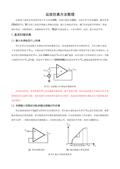
1直流扫描仿真1.1输入失调电压(V OS)仿真图1-1所示为运放输入失调电压的实际测量方法。
将运放接成单位负反馈的形式,并在正输入端加一个合适的直流电平V CM。
只要运放开环增益足够大则输出端电压即为输入直流电平加上输入失调电压。
由此可很方便地测量得到V OS。
实际CMOS运放的V OS约为mV量级,由非无限大开环增益引入的正、负输入端的压差为V CM/(1+A),因此对于增益大于10000(80dB)的运放该误差对V OS测量造成的影响可以忽略。
图1-1运放输入失调电压测量结构必须注意的是,仿真得到的V OS仅由偏置失配造成,属于系统失调。
实际运放的输入失调电压的主要影响因素为元器件失配,而仿真器中会假设所有器件完全相同,因此仿真得到的失调电压并不能准确表征实际情况。
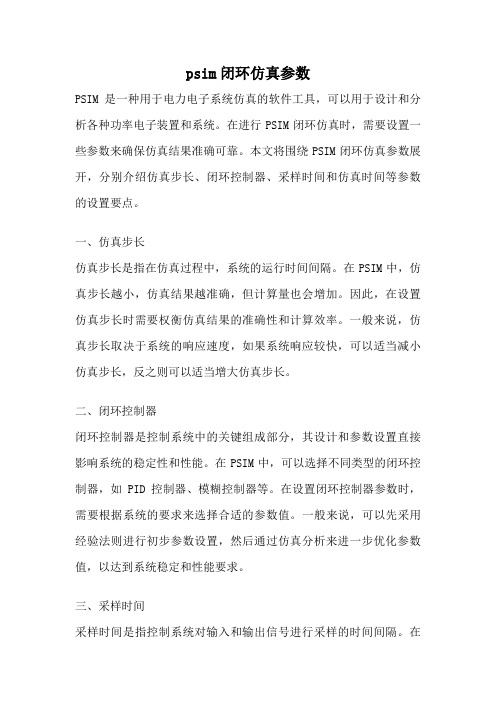
1.2共模输入范围(ICMR)和输出摆幅(SW)仿真将运放接成如图1-2(a)所示的单位负反馈的形式,将正输入端的电压从0至V DD进行直流扫描,观察输出端的电压变化曲线,即可观察该单位缓冲器的线性范围。
在运放的线性工作区域内,直流扫描曲线的斜率为45°,即输出能够良好跟随输入;在线性范围之外,则曲线发生弯曲,如图1-2(b)所示。
(a)仿真电路结构(b)输出随输入变化曲线图1-2输入共模范围仿真用该结构仿真得到的线性范围同时受到输入共模范围和输出摆幅的限制,因此无法用该结构精确测得ICMR。
对于一般的运放,输出摆幅范围通常大于输入共模范围,故该方法能够大致预估输入共模范围。
图1-3(a)所示的反相电压放大器增益为-10。
psim闭环仿真参数
psim闭环仿真参数PSIM是一种用于电力电子系统仿真的软件工具,可以用于设计和分析各种功率电子装置和系统。
在进行PSIM闭环仿真时,需要设置一些参数来确保仿真结果准确可靠。
本文将围绕PSIM闭环仿真参数展开,分别介绍仿真步长、闭环控制器、采样时间和仿真时间等参数的设置要点。
一、仿真步长仿真步长是指在仿真过程中,系统的运行时间间隔。
在PSIM中,仿真步长越小,仿真结果越准确,但计算量也会增加。
因此,在设置仿真步长时需要权衡仿真结果的准确性和计算效率。
一般来说,仿真步长取决于系统的响应速度,如果系统响应较快,可以适当减小仿真步长,反之则可以适当增大仿真步长。
二、闭环控制器闭环控制器是控制系统中的关键组成部分,其设计和参数设置直接影响系统的稳定性和性能。
在PSIM中,可以选择不同类型的闭环控制器,如PID控制器、模糊控制器等。
在设置闭环控制器参数时,需要根据系统的要求来选择合适的参数值。
一般来说,可以先采用经验法则进行初步参数设置,然后通过仿真分析来进一步优化参数值,以达到系统稳定和性能要求。
三、采样时间采样时间是指控制系统对输入和输出信号进行采样的时间间隔。
在PSIM中,采样时间的设置与控制器的采样时间一致,通常需要根据被控对象的特性和控制要求来确定。
如果采样时间过长,可能会导致系统响应不及时,影响系统的稳定性和性能;如果采样时间过短,可能会增加控制器计算的复杂度,降低系统的控制精度。
因此,在设置采样时间时需要综合考虑系统的要求和计算复杂度。
四、仿真时间仿真时间是指仿真过程中系统运行的时间长度。
在PSIM中,仿真时间的设置应根据仿真目的来确定。
如果只是进行短暂的系统响应分析,可以设置较短的仿真时间;如果需要进行长时间的系统稳定性和性能分析,可以设置较长的仿真时间。
同时,还需要注意仿真时间与仿真步长之间的关系,确保仿真结果的准确性和计算效率。
PSIM闭环仿真参数的设置对于系统设计和分析至关重要。
通过合理设置仿真步长、闭环控制器、采样时间和仿真时间等参数,可以得到准确可靠的仿真结果。
PSIM仿真(一)
1.1实验目的
1、掌握PSIM软件的基本使用方法;
2、掌握PSIM软件中元器件的摆放、连接的简单操作;
3、掌握仿真电路图构建界面的创建流程,以及仿真结果输出界面的使用。
1.2实验原理
本实验通过对Buck电路的开环仿真,来熟悉PSIM软件的环境及仿真电路图构建界面的创建流程和仿真结果输出界面的使用。
7.改变开关频率为200Hz,看上述的波形有何不同,试分析和理解相关的原因。
8.改变输出电感为1mL到0.1mL观察上述波形有何不同。
1.5提高题
试分析下图图7的电路工作过程,并根据以上Buck电路的PSIM仿真方法,搭建以下电路,通过仿真分析该电路图的功能,分析该电路的工作过程,推导出输出电压和输入电压之间的关系,并通过仿真验证。
C、依次放置所需元件。
3.创建完成的仿真电路图,分别修改元件参数
(提示:仿真时间模块位于simulate--simulation contro)
图4
3、点击仿真按钮,仿真编译
图5
三种方法:
A、Simulate-> Run Simulation;
B、左侧仿真按钮;
C、F8。
4、仿真波形图的建立
图6
6.通过仿真得到在上述电路情况下,调节电路的关键参数得到12V的输出电压,此时开关管两端的波形,负载电压和电流波形。
1.3实验内容
(1)认识和熟悉PSIM软件的界面和操作方法
(2)用PSIM软件对Buck电路进行开环仿真。
电路原理图:
图1
1.4实验步骤
1、创建一个新的文件,并保存
图2
2、分别选择连续点左键即可连续放置相同元件,如要取消则按Esc;
运放稳定性的SPICE仿真
运放稳定性的SPICE仿真SPICE是一种检查电路潜在稳定性问题的有用工具。
本文将介绍一种使用SPICE工具来检查电路潜在稳定性的简单方法。
图1是使用OPA211 搭建的一个同相放大器,在许多应用中,只是对图1做了较小的变动。
R3和C1构成了输入级滤波器。
R4是电路的输出电阻,当运放输出级连接到其它外部电路时,R4起到保护作用。
CL用来等效5英尺电缆。
该电路的小信号阶跃响应或者方波的响应曲线是检查潜在稳定性问题的最快捷和最简单的方法。
图2是仿真电路。
值得注意的是电路输入端连接到地,输入测试信号源直接连接到运放的同相输入端。
输入级的滤波器将延缓输入信号的边沿。
如果你想知道一个钟是如何产生铃声的,你应该使用一个铁锤敲击它,而不是一个橡皮棒。
响应曲线是在运放的输出端探测,而不是电路的Vout节点。
R4和CL构成了滤波器以至于Vout节点不能真正地显示出运放的过冲。
为了检查稳定性,我们需要知道运放是如何工作的。
注意到输入信号的幅度是1mV(在运放输出端的幅度是4mV)。
我们希望得到小信号的响应曲线。
若输入信号是大信号,则会涉及到压摆率的问题,将减小过冲,不能真正地反应潜在的不稳定性。
从仿真结果可以看出,在运放的输出端有接近27%的过冲,较大的过冲会导致运放在任何条件下都是不稳定的。
假设这是一个二阶稳定系统,它意味着接近38度的相移裕量。
另外,注意到频率响应曲线中存在相当大的尖峰,这是另一个潜在的不稳定的迹象。
幅度峰值在14MHz时出现,其正好是时域上振铃周期的倒数。
普遍认为,当信号的过冲小于或等于20%时,相移裕量大于或。
《运放基本仿真步骤》课件

PART FOUR
设置仿真参数,如时间、频 率、电压等
建立仿真模型,包括输入、 输出、运算等模块
打开仿真软件,如MATL AB、 Simulink等
运行仿真程序,观察仿真结 果,如波形、数据等
分析仿真结果,验证设计是 否满足要求
调整仿真参数,重新运行仿 真程序,直至满足设计要求
观察输出电压波形:观察输出电压波形的 形状、幅度、频率等参数是否符合预期
观察输入电流波形:观察输入电流波形的 形状、幅度、频率等参数是否符合预期
观察输入电压波形:观察输入电压波形的 形状、幅度、频率等参数是否符合预期
观察电路参数:观察电路参数(如电阻、 电容、电感等)的变化是否符合预期
观察输出电流波形:观察输出电流波形的 形状、幅度、频率等参数是否符合预期
搭建仿真电路:根据实际需求,搭建运放电 路,包括输入、输出、反馈等部分
设置仿真参数:设置仿真时间、步长、精度 等参数,确保仿真结果的准确性
运行仿真:运行仿真,观察输出波形,分析 运放性能
调整参数:根据仿真结果,调整电路参数, 优化运放性能
保存结果:保存仿真结果,以便后续分析或 与其他人分享
PART TWO
仿真模型搭建:搭建符合实际需求的仿真 模型
参数设置:设置合理的参数值和范围
仿真结果分析:分析仿真结果,找出影响 性能的关键参数
参数调整:根据分析结果,调整关键参数值
重复仿真:重复进行仿真,直至达到满意 的性能指标
调整参数:根据仿 真结果调整参数, 如增益、带宽等
优化模型:选择合 适的模型,如 SPICE、Hspice等
,
汇报人:
CONTENTS
- 1、下载文档前请自行甄别文档内容的完整性,平台不提供额外的编辑、内容补充、找答案等附加服务。
- 2、"仅部分预览"的文档,不可在线预览部分如存在完整性等问题,可反馈申请退款(可完整预览的文档不适用该条件!)。
- 3、如文档侵犯您的权益,请联系客服反馈,我们会尽快为您处理(人工客服工作时间:9:00-18:30)。
Op-Amp Simulation – Part II EE/CS 5720/6720This assignment continues the simulation and characterization of a simple operational amplifier. Turn in a copy of this assignment with answers in the appropriate blanks, and Cadence printouts attached. All problems to be turned in are marked in boldface.For the following problems, use the two-stage op amp you simulated in the previous assignment, using the same value of C C and the same lead compensation transistor you arrived at. For all simulations below, load the amplifier with R L = 1M Ω in parallel with C L = 30pF.1. Common-mode gain; CMRRCommon-mode gain measures how much the output changes in response to a change in the common-mode input level. Ideally, the common-mode gain of an op amp is zero; the amplifier should ignore the common-mode level and amplify only the differential-mode signal. Let’s measure the common-mode gain of our op amp.In order to measure the common-mode gain in the open-loop condition, we have to once again “balance” our high-gain op amp very carefully to keep V OUT ≈ 0, just like we did in the last assignment when we measured the transfer function. Remember, we do this by adding a dc voltage source V OS in series with one of the inputs. This voltage source is set to the input offset voltage so that if no other signal is present, the output voltage will be approximately zero. Now, with this adjustment in place, we tie the two inputs together and apply an ac signal v IN , as shown below.Lv OUTv IN V OSPlot the common-mode gain (in dB) transfer function of the op amp over the frequency range 1Hz – 100MHz. Plot at least 50 points per decade of frequency for good resolution. Turn in this plot.What is the common-mode gain at 10 Hz? ____________________What is the common-mode gain at 100 kHz? ____________________An important figure of merit in op amp design is the common-mode rejection ratio , or CMRR . CMRR is defined as the differential-mode gain divided by the common-mode gain. (Remember, if you express your gains in the logarithmic units of dB, subtraction isequivalent to division.) For example, if a particular amplifier has a differential gain of 80 dB at 100 Hz and a common-mode gain of 10 dB at the same frequency, then the amplifier’s CMRR at 100 Hz is 70 dB. Ideally, an amplifier should have infinite CMRR. Practically, most designers try to get CMRR > 60 dB, though some applications may required much higher values.Disconnect the negative input of the op amp from v IN and connect it back to ground. Measure the differential-mode gain (in dB) transfer function of the op amp over the frequency range 1Hz – 100MHz. (This is the same measurement you did in the last assignment.) Plot at least 50 points per decade of frequency for good resolution. Turn in this plot.What is the CMRR at 10 Hz (in dB)? ____________________What is the CMRR at 100 kHz (in dB)? ____________________2. Alternate method for measuring open-loop transfer functionThe previous method we used for measuring transfer functions can become slow and tedious if we often make changes to our op amp that affect its dc operating point, because this requires re-measuring the small dc offset voltage, which will have changed. Luckily, changing the value of C C has no affect on the dc bias point, so we haven’t had to repeat the dc offset measurements yet. However, if we make any changes to transistor sizes or bias currents, we would have to repeat the dc sweep to find V OS before measuring the transfer function again.It turns out there is an easier way to measure open-loop transfer functions that does not require us to measure V OS and then “balance” the open-loop op amp. The measurement configuration is shown below.Lv OUT v INFirst, we make R >> R L so that this resistor has no significant loading effect on the op amp. Let’s set R = 100M Ω in our simulation.Here’s how this configuration works: At dc (and very low frequencies), C is basically an open circuit. Since no current flows into the op amp’s inputs (or through C ), the current through R is zero. That means the voltage drop across R is also zero, so the voltage at the negative input of the op amp is equal to the output voltage. Thus, at very low frequencies, the op amp is configured at a unity-gain buffer, so v OUT ≅ v IN . If we make the dc value of v IN = 0, then our output is where we want it to be.At high frequencies, the reactance of C (1/j ωC ) becomes very small relative to the resistance of R (i.e., the capacitor begins to act like a short circuit), and so the negative input is effectively connected to ground, just like in our previous open-loop measurements. The key is to set C sufficiently high so that the effects caused by the RC network occur at frequencies far below what you actually want to measure. The effect of the RC network on the amplifier gain curve is shown below. At very low frequencies, the amplifier starts to act like a unity-gain buffer.V A |ωWe should set C such that the frequency A V /(2πRC ) << f min , where A V is the low-frequency gain of the op amp, and f min is the minimum frequency of interest in our transfer functions.Set C = 0.1 F (that’s right: one-tenth of a Farad!). Run an ac simulation from 1nHz (that’s right: one nanoHertz!) to 100MHz, showing gain (in dB) and phase. Turn in this plot. On the plot, label the two frequencies shown on the above figure. Do the calculated frequencies match the appropriate points on the curve? _______________ (Remember to convert radians/second to Hz, if necessary.)Now run an ac simulation just from 1Hz to 100MHz, showing gain (in dB) and phase. Turn in this plot.How does this gain plot compare with the differential-mode gain curve measured in the previous problem using the traditional method? ___________________________ ________________________________________________________________________ ________________________________________________________________________3. Slew rateIn the previous assignment, we used ac analysis to determine the small-signal bandwidth of the op amp. The speed of amplifiers is often limited by large-signal effects such as slew rate – the maximum speed at which an op amp can charge and discharge its load. To measure slew rate, configure the op amp as a unity-gain buffer as shown below.Lv OUT v INRun a transient simulation where v IN is a 5 kHz square wave going from -1V to +1V. (This qualifies as a large signal.) Look at the output waveform. Does it look like a nice square wave, or do you see significant slewing (a slope less than infinity) on the -1V to +1V transitions? Increase the frequency of the square wave until you can see these sloped regions clearly. (The output should still reach -1V and +1V during each cycle. If it does not, your square wave is too fast.) Make sure your maximum time step is at least 200 times less than your simulation time so you get a high-resolution simulation. Turn in this plot.Now select two points on the rising slope and from these calculate the positive slew rate using units of V/µs.The positive slew rate is ___________________.Now select two points on the falling slope and from these calculate the negative slew rate using units of V/µs.The negative slew rate is ___________________.Now repeat the above measurements after removing R L and C L . Turn in this slew-rate plot.The positive slew rate with no load is ___________________.The negative slew rate with no load is ___________________.What is the slew rate predicted by Equation 5.15 in Johns & Martin? ________________. How does this compare with the simulation results? ______________________________ ________________________________________________________________________4. Output resistanceNow we will estimate the closed-loop output resistance of our op amp in unity gain configuration. Keep the same circuit setup as above, but remove R L from the circuit and make the input waveform a small 1kHz sine wave with a dc level of zero volts and an amplitude of 1mV. (Use a transient source, not the “AC” source. We will be running transient simulations.) Run a simulation of encompassing 2-3 cycles of the waveform and verify that the output amplitude matches the input amplitude. Turn in this plot. If you wish, you can insert a dc V OS source at the input to cancel out any small offset voltage.Now add R L = 1M Ω back to the circuit. Make sure R L is connected to ground, not V SS . Run the simulation again.What is the output voltage amplitude? _______________________Now decrease the value of R L until the output voltage amplitude drops to approximately 0.909mV instead of 1.0mV.What value of R L causes an output amplitude of 0.909mV? ___________________ Based on a simple voltage divider relationship, what must the output resistance of the unity-gain buffer be? ________________________Using the low-frequency open-loop gain amplifier gain measured in previous problems, what would you predict the open-loop output resistance of the op amp to be? ________________What would you predict the output resistance of the amplifier to be if it were configured (with an appropriate feedback network) to have a closed-loop gain of 1000? ____________________。