TI(德州仪器)公司产品导购手册
Texas Instruments SLUU068C 用户指南说明书

IMPORTANT NOTICETexas Instruments Incorporated and its subsidiaries (TI) reserve the right to make corrections, modifications, enhancements, improvements, and other changes to its products and services at any time and to discontinue any product or service without notice. Customers should obtain the latest relevant information before placing orders and should verify that such information is current and complete. All products are sold subject to TI’s terms and conditions of sale supplied at the time of order acknowledgment.TI warrants performance of its hardware products to the specifications applicable at the time of sale in accordance with TI’s standard warranty. T esting and other quality control techniques are used to the extent TI deems necessary to support this warranty. Except where mandated by government requirements, testing of all parameters of each product is not necessarily performed.TI assumes no liability for applications assistance or customer product design. Customers are responsible for their products and applications using TI components. T o minimize the risks associated with customer products and applications, customers should provide adequate design and operating safeguards.TI does not warrant or represent that any license, either express or implied, is granted under any TI patent right, copyright, mask work right, or other TI intellectual property right relating to any combination, machine, or process in which TI products or services are used. Information published by TI regarding third−party products or services does not constitute a license from TI to use such products or services or a warranty or endorsement thereof. Use of such information may require a license from a third party under the patents or other intellectual property of the third party, or a license from TI under the patents or other intellectual property of TI.Reproduction of information in TI data books or data sheets is permissible only if reproduction is without alteration and is accompanied by all associated warranties, conditions, limitations, and notices. Reproduction of this information with alteration is an unfair and deceptive business practice. TI is not responsible or liable for such altered documentation.Resale of TI products or services with statements different from or beyond the parameters stated by TI for that product or service voids all express and any implied warranties for the associated TI product or service and is an unfair and deceptive business practice. TI is not responsible or liable for any such statements.Mailing Address:Texas InstrumentsPost Office Box 655303Dallas, Texas 75265Copyright 2001, Texas Instruments IncorporatedEVM IMPORTANT NOTICETexas Instruments (TI) provides the enclosed product(s) under the following conditions:This evaluation kit being sold by TI is intended for use for ENGINEERING DEVELOPMENT OR EVALUATION PURPOSES ONLY and is not considered by TI to be fit for commercial use. As such, the goods being provided may not be complete in terms of required design-, marketing-, and/or manufacturing-related protective considerations, including product safety measures typically found in the end product incorporating the goods. As a prototype, this product does not fall within the scope of the European Union directive on electromagnetic compatibility and therefore may not meet the technical requirements of the directive.Should this evaluation kit not meet the specifications indicated in the EVM User’s Guide, the kit may be returned within 30 days from the date of delivery for a full refund. THE FOREGOING WARRANTY IS THE EXCLUSIVE WARRANTY MADE BY SELLER TO BUYER AND IS IN LIEU OF ALL OTHER WARRANTIES, EXPRESSED, IMPLIED, OR STATUTORY, INCLUDING ANY WARRANTY OF MERCHANTABILITY OR FITNESS FOR ANY PARTICULAR PURPOSE.The user assumes all responsibility and liability for proper and safe handling of the goods. Further, the user indemnifies TI from all claims arising from the handling or use of the goods. Please be aware that the products received may not be regulatory compliant or agency certified (FCC, UL, CE, etc.). Due to the open construction of the product, it is the user’s responsibility to take any and all appropriate precautions with regard to electrostatic discharge.EXCEPT TO THE EXTENT OF THE INDEMNITY SET FORTH ABOVE, NEITHER PARTY SHALL BE LIABLE TO THE OTHER FOR ANY INDIRECT, SPECIAL, INCIDENTAL, OR CONSEQUENTIAL DAMAGES.TI currently deals with a variety of customers for products, and therefore our arrangement with the user is not exclusive.TI assumes no liability for applications assistance, customer product design, software performance, or infringement of patents or services described herein.Please read the EVM User’s Guide and, specifically, the EVM Warnings and Restrictions notice in the EVM User’s Guide prior to handling the product. This notice contains important safety information about temperatures and voltages. For further safety concerns, please contact the TI application engineer.Persons handling the product must have electronics training and observe good laboratory practice standards. No license is granted under any patent right or other intellectual property right of TI covering or relating to any machine, process, or combination in which such TI products or services might be or are used.Mailing Address:Texas InstrumentsPost Office Box 655303Dallas, Texas 75265Copyright 2001, Texas Instruments IncorporatedEVM WARNINGS AND RESTRICTIONSIt is important to operate this EVM within the input voltage range of 85 V to 265 V and the output voltage of 12 V +/− 5%.Exceeding the specified input range may cause unexpected operation and/or irreversible damage to the EVM. If there are questions concerning the input range, please contact a TI field representative prior to connecting the input power.Applying loads outside of the specified output range may result in unintended operation and/or possible permanent damage to the EVM. Please consult the EVM User’s Guide prior to connecting any load to the EVM output. If there is uncertainty as to the load specification, please contact a TI field representative.During normal operation, some circuit components may have case temperatures greater than 50°C. The EVM is designed to operate properly with certain components above 50°C as long as the input and output ranges are maintained. These components include but are not limited to linear regulators, switching transistors, pass transistors, and current sense resistors. These types of devices can be identified using the EVM schematic located in the EVM User’s Guide. When placing measurement probes near these devices during operation, please be aware that these devices may be very warm to the touch.Mailing Address:Texas InstrumentsPost Office Box 655303Dallas, Texas 75265Copyright 2001, Texas Instruments IncorporatedContentsContents. . . . . . . . . . . . . . . . . . . . . . . . . . . . . . . . . . . . . . . . . . . . . . . . . . . . . . . . . . . . .1General Information1-1 . . . . . . . . . . . . . . . . . . . . . . . . . . . . . . . . . . . . . . . . . . . . . . . . . . . . . . . . . . . . . . . . . .1.1Features1-2. . . . . . . . . . . . . . . . . . . . . . . . . . . . . . . . . . . . . . . . . . . . . . . . . . . . . . . . . . . . . . . .1.2Description1-2. . . . . . . . . . . . . . . . . . . . . . . . . . . . . . . . . . . . . . . . . . . . . . . . . . . . . . . .1.3Operating Guidelines1-3. . . . . . . . . . . . . . . . . . . . . . . . . . . . . . . . . . . . . . . . . . . .1.3.1Step 1. Load Connections1-3. . . . . . . . . . . . . . . . . . . . . . . . . . . . . . . . . . . . . . . . .1.3.2Step2. Applying Input Power1-3. . . . . . . . . . . . .1.3.3Step 3. Evaluating the Demonstration’s Boards Performance.1-3. . . . . . . . . . . . . . . . . . . . . . . . . . . . . . . . . . . . . . . . . . . . . . . .1.3.4Additional Information1-3. . . . . . . . . . . . . . . . . . . . . . . . . . . . . . . . . . . . . . . . . . . . . . . . .1.4DM38500 EVM Performance1-5. . . . . . . . . . . . . . . . . . . . . . . . . . . . . . . . . . . . . . . . . . . . . . . . . . . . . . . . . . . . . . . . . . . . . . .2Reference2-1. . . . . . . . . . . . . . . . . . . . . . . . . . . . . . . . . . . . . . . . . . . . .2.1DM38500 EVM Part Descriptions2-2. . . . . . . . . . . . . . . . . . . . . . . . . . . . . . . . . . . . . . . . . . . . . . . . . . . .2.2DM38500 Board Layouts2-4Figures. . . . . . . . . . . . . . . . . . . . . . . . . . . .1−1.DM38500 Evaluation Module Application Schematic1-4. . . . . . . . . . . . . . . . . . . . . . . . . . . . . . . . . . . . . .1−2.DM38500 EVM Response, VCC = +15 V1-5. . . . . . . . . . . . . . . . . . . . . . . . . . . . . . . . . . . . . . . . . . .1−3.DM38500 Response, VCC = +15 V1-5. . . . . . . . . . . . . . . . . . . . . . . . . . . . . . . . . . . . . . . . . . .1−4.DM38500 Response, VCC = +15 V1-6. . . . . . . . . . . . . . . . . . . . . . . . . . . . . . . . . . . . . .2−1.DM38500 EVM PC Board: Top Assembly2-4Chapter 1GeneralInformationThis chapter details the Texas Instruments (TI) DM38500 PFC/PWM Combination Controller 100W Power Factor Correction Preregulator Evaluation Module (EVM) SLUU068. It includes a list of EVM features, a brief description of the module illustrated with a pictorial, schematic diagrams, and EVM specifications.Topic Page . . . . . . . . . . . . . . . . . . . . . . . . . . . . . . . . . . . . . . . . . . . . . . . . . . . . .1.1Features1−2. . . . . . . . . . . . . . . . . . . . . . . . . . . . . . . . . . . . . . . . . . . . . . . . . . .1.2Description1−2 1.3Operating Guidelines1−3. . . . . . . . . . . . . . . . . . . . . . . . . . . . . . . . . . . . . . . . . .1.4DM38500 EVM Performance1−5. . . . . . . . . . . . . . . . . . . . . . . . . . . . . . . . . . . .General Information1-1Features1.1FeaturesUCC38500 PFC/PWM Combination Controller 100W Power Factor Correc-tion Preregulator include:J Combines PFC and 2nd Stage Down Converter ControlsJ Controls Boost Preregulator to Near-unity Power FactorJ Accurate Power LimitingJ Improved Feedforward Line RegulationJ Peak Current Mode Control in Second StageJ Programmable OscillatorJ Leading Edge/Trailing Edge Modulation for Reduced Output RippleJ Low Startup Supply CurrentJ Synchronized Second Stage with Programmable Soft-startJ Programmable Second Stage Shut-down1.2DescriptionThe UCC38500 provides all the functions necessary for active power factorcorrection and a second stage dc-to-dc converter all in one integrated circuit.The control IC uses leading edge modulation for the boost stage and trailingedge modulation for the step down converter to reduce the RMS current in theboost capacitor. The dc-to-dc controller uses peak current mode control foreasy loop compensation.The UCC38500 evaluation board is designed to illustrate the performance ofthe IC in a complete off-line 100W two-stage power converter using power fac-tor correction. The demonstration board was designed to operate with a uni-versal input voltage range (i.e. 85−265 Vac) with a regulated 12V dc output.CautionHigh-voltage levels are present on the evaluation module whenever it isenergized. Proper precautions must be taken when working with theEVM. The output capacitor has high levels of energy storage and it mustbe discharged before the load is removed. Serious injury can occur ifproper safety precautions are not followed.1-2Description1-3General Information 1.3Operating GuidelinesThe operating guidelines for the evaluation board are provided with reference to the schematic in Figure 1−1 and the component layout in Figure 2−1.1.3.1Step 1. Load ConnectionsA resistive or electronic load can be applied to the output terminals labeled OUT− and OUT+.Note: For safety reasons the load should be connected before power is sup-plied to the demonstration board.1.3.2Step2. Applying Input PowerA 60 Hz AC power source not exceeding 265 V RMS needs be applied across terminals AC−N and AC−L for proper operation.1.3.3Step 3. Evaluating the Demonstration’s Boards Performance.With the AC source set between 85−265 V RMS the output voltage should be regulated and the input current should track the input voltage shape with near unity power factor. The operation of the circuit is verified over the line and load range and shows efficiency as high as 85%. At lighter loads, there may be some distortion in the line current due to Discontinuous Conduction Mode (DCM) operation. Please refer to Figures 1−2, 1−3 and 1−4 for typical EVM performance.1.3.4Additional InformationFor more information, pin description and specifications for the UCC38500PFC/PWM Combination Controller, please refer to the datasheet or contact the Texas Instruments Semiconductor Product Information Center at 1-800-336-5236 or 1-972-644-5580. Product Information can also be found on the World Wide Web at .Description1-4Figure 1−1.DM38500 Evaluation Module Application SchematicUDG−000941210952611137843116171518191420O V P /E N B L V S E N S E V A O U T I S E N S E M O U TC A O U T I A C V F FP K L I M I T V R E F G T 1G T 2V C C C T R T G N D P W R G N D S S 2V E R R I S E N S E 2U C C 38500V R E FQ 5R 25V C CR 7R 6G T 1G T 2D 10D 9C 27P K L I M I TC 28R 17C 19C 22R 28C 25R 23R 34R 21R 22R 33R 20C 2R 15R 5L 1D 3D 1G T 1R 14R 29P K L I M I TR 19C 26V R E F R 18R 24C 29C 30I S E N S E 2G T 2R 13R 2C 5P W R G N D G T 212 V 100 W +−L 2T 1Q 2Q 1Q 3D 11V A C 85−265V R M SD 6D 4T 2D 8U 4C 7S G N DS G N D S G N DP G N D 2P G N DP G N DP G N DP G N DS G N D P G N D D 5D 7C 12C 20L 1V C C B I A S C I R C U I TV C CV C C B I A S C I R C U I TP G N D C 23P G N D 2P G N D 2R 26D 14R 36R 16C 14R 35R 32R 27D 13R 31C 8R 30R 10R 12R 11C 21C 16C 3P G N D C 24D 2R 1C 4C 18R 4D 15D 12D 16A C −NA C −LO U T +O U T −V R E FR 3R 39C 13I S E N S E 2C 17H 11A V 1321456U 3S G N D C 6C 38H I G H V O L T A G E −S E E E V M W A R N I N G S A N D R E S T R I C T I O N SH I G H T E M P E R A T U R E −S E E E V M W A R N I N G S A N D R E S T R I C T I O N SH I G H V O L T A G E −S E E E V M W A R N I N G S A N D R E S T R I C T I O N S H I G H T E M P E R A T U R E −S E E E V M W A R N I N G S A N D R E S T R I C T I O N S Note: High-Voltage component. See EVM Warnings and Restrictions at the back of this document. Note: High-T emperature component. See EVM Warnings and Restrictions at the back of this document.DM38500 EVM Performance1-5General Information 1.4DM38500 EVM PerformanceFigure 1−2 through 1−4 shows the typical evaluation module performance.Figure 1−2.DM38500 EVM EfficiencyUCC38500 EFFICIENCYvsOUTPUT POWER 505560657075808590201040306050807090100V IN = 85 VV IN = 175 VV IN = 265 VP OUT − WE f f i c i e n c y −%Figure 1−3.DM38500 Power FactorUCC38500 PFvsOUTPUT POWERP OUT − WP o w e r F a c t o r0.852010403060508070901000.900.951.00V IN = 85 V V IN = 175 VV IN = 265 VDM38500 EVM Performance1-6Figure 1−4.DM38500 Total Harmonic Distortion5101520253020104030605080709010035UCC38500 TOTAL HARMONIC DISTORTIONvsOUTPUT POWERP OUT − WT o t a l H a r m o n i c D i s t o r t i o nV IN = 85 VV IN = 175 VV IN = 265 V2-1ReferenceReferenceThis chapter includes a parts list and PCB layout illustrations for the DM38500EVM.TopicPage2.1DM38500 EVM Part Descriptions 2−2. . . . . . . . . . . . . . . . . . . . . . . . . . . 2.2DM38500 Board Layouts 2−4. . . . . . . . . . . . . . . . . . . . . . . . . . . . . . . . . . Chapter 2DM38500 EVM Part Descriptions2-22.1DM38500 EVM Part DescriptionsTable 2−1.DM38500 Part DescriptionsDescriptionReference Qty Value/Type Number Manufacturer Part Number C12, C20,C293 1 µF, 50 V, polypropylene Panasonic ECQ−V1H105JL C13147 pF, 50 V, ceramic Panasonic ECU−S2A470JCA C7, C16,C14310 nF, 50 V, ceramic Panasonic ECU−S1H103JCB C17, C382100 pF, 50 V, ceramic Panasonic ECU−S1H101JCA C191 2.2 nF, 50 V, ceramic Panasonic ECU−S1H222JCB C21470 nF, 400 V, polypropylenePanasonic ECQ−E4474KZ C211680 pF, 50 V, ceramic Panasonic ECU−S1H681JCB CapacitorsC221390 pF, 50 V, ceramic Panasonic ECU−S1H391JCA C241100 pF, 50 V, ceramic Panasonic ECU−S1H101JCA C251150 nF, 50 V, ceramicPanasonic ECU−S1H154KBB C26147 nF, 600 V, polypropylene Panasonic ECQ−E6473KF C27, C182100 pF, 50 V, ceramic Panasonic ECU−S1H105KBB C28, C232 2.2 µF, 50 V, ceramicPanasonic ECU−S1H225MEB C31100 µF, 450 V, electrolytic Panasonic ECO−S2WB101BA C3011800 µF, 25 V, electrolytic Panasonic ECA−IEFQ182C4, C5, C830.1 µF, 50 V, ceramic Panasonic ECU−S1H104KBB C61100 µF, 25 V, electrolytic Panasonic EEU−FCIE101S D11 6 A, 600 V, GI756CTGeneral Inst.GI756CT D111 6 A, 600 V, bridge rectifier,PB66Diodes Inc.PB66D121 1 A, 40 V, Shottky SR103CT D131TL431CLPTITL431C D14110 V, 1 W, Zener 1N4740D15, D2218 V, 1 W, Zener 1N4746DiodesD31 6 A, 600 V, ultra fast IR HFA08TB60−ND D4, D62 1 A, 600 V, fast recovery PhilipsBYV26C D5,D7,D9,D10, D165 1 A, 40 V, Shottky 1N5819D81 6 A, 600 V, full wave rectifierIRHBR2045FH1, FH223AG Fuse clip Fuses F11 6 A, 250 V HS31For Q3Aavid 513201HS4, HS52For D3 and D8Aavid 579302 B 0 00 00Heat sinks HS1, HS22For Q1 and Q2Avid 593002 B 0 34 00L11 1.7 mH, 2.5 A, coupled Cooper CTX08−14730Inductors L2135 µH, 8.3 ACooper CTX08−14279Q1,Q228 A, 500 V, n−channel IR IRF840Q3114 A, 500 V, n−channel IRIRFP450MOSFETsQ51NPN transistor MJE13005Not usedQ4, R8, R9,C9, C15,C106Not usedDM38500 EVM Part Descriptions2-3Reference DescriptionReference Qty Value/Type Number ManufacturerPart Number R1, R122ShortR10, R362200 Ω, ¼ W R25, R29,R27310 k Ω, ¼ WR131 2 k Ω, ¼ W R141 1.5 k Ω, ¼ W R15, R192 3.92 k Ω, ¼ W R161750 Ω, ¼ W R1717.5 k Ω, ¼ W R18, R242392 k Ω, ¼ W R2, R112 1 k Ω, ¼ W R20122.1 k Ω, ¼ W R2118.25 k Ω, ¼ W R22, R332562 k Ω, ¼ W ResistorsR231200 k Ω, ¼ W R261100 Ω, ¼ WR281100 k Ω, ¼ W R30130.1 k Ω, ¼ W R31133.2 k Ω, ¼ W R321 4.75 k Ω, ¼ W R341221 k Ω, ¼ W R35116.2 k Ω, ¼ W R391 1 k Ω, 1 W R41 1 Ω, 1 W, ±5%R510.33 Ω, 3 W, ±5%R6, R7220 Ω, ¼ WR3151 k Ω, 2 W, 400 VT118 mH, 10 A, 10.8:1Cooper CTX08−14226Transformers T21560−990 µH, 1:1 gate drive Cooper CTX08−14225U41BiCMOS PFC/PWM combination controller TexasInstrumentsUCC38500N ICsU31Opto-isolator4N36X13Thermal pad TO−220(@ Q1, Q2, D8)X21Thermal pad TO−247(@ Q3)MiscellaneousX34Screw pan head #4−40 X 7/16 (@Q1, Q2, Q3, D8)X44Nut #4x40X53Nylon shoulder washer #4(@Q1, Q2, D8)X61Bevel washer #4 (@Q3)PCBPCB1Bare boardUCC38500 PCBNotes:1)The values of these components are to be determined by the user in accordance with the applica-tion requirements.2)Unless otherwise specified, all resistors have a tolerance of ±1%.3)Capacitor C38 is located at reference designator R38 on the PCB.。
德州仪器(TI)LM3S2793系列规格书,Datasheet资料
TEXAS INSTRUMENTS-PRODUCTION DATAStellaris®LM3S2793MicrocontrollerDATA SHEETCopyright©2007-2012 DS-LM3S2793-11425CopyrightCopyright©2007-2012Texas Instruments Incorporated All rights reserved.Stellaris and StellarisWare®are registered trademarks of Texas Instruments Incorporated.ARM and Thumb are registered trademarks and Cortex is a trademark of ARM Limited.Other names and brands may be claimed as the property of others.PRODUCTION DATA information is current as of publication date.Products conform to specifications per the terms of Texas Instruments standard warranty.Production processing does not necessarily include testing of all parameters.Please be aware that an important notice concerning availability,standard warranty,and use in critical applications of Texas Instruments semiconductor products and disclaimers thereto appears at the end of this data sheet.Texas Instruments Incorporated108Wild Basin,Suite350Austin,TX78746/stellaris/sc/technical-support/product-information-centers.htmStellaris®LM3S2793MicrocontrollerTable of ContentsRevision History (32)About This Document (43)Audience (43)About This Manual (43)Related Documents (43)Documentation Conventions (44)1Architectural Overview (46)1.1Overview (46)1.2Target Applications (48)1.3Features (48)1.3.1ARM Cortex-M3Processor Core (48)1.3.2On-Chip Memory (50)1.3.3External Peripheral Interface (51)1.3.4Serial Communications Peripherals (53)1.3.5System Integration (57)1.3.6Advanced Motion Control (63)1.3.7Analog (65)1.3.8JTAG and ARM Serial Wire Debug (66)1.3.9Packaging and Temperature (67)1.4Hardware Details (67)2The Cortex-M3Processor (68)2.1Block Diagram (69)2.2Overview (70)2.2.1System-Level Interface (70)2.2.2Integrated Configurable Debug (70)2.2.3Trace Port Interface Unit(TPIU) (71)2.2.4Cortex-M3System Component Details (71)2.3Programming Model (72)2.3.1Processor Mode and Privilege Levels for Software Execution (72)2.3.2Stacks (72)2.3.3Register Map (73)2.3.4Register Descriptions (74)2.3.5Exceptions and Interrupts (87)2.3.6Data Types (87)2.4Memory Model (87)2.4.1Memory Regions,Types and Attributes (89)2.4.2Memory System Ordering of Memory Accesses (90)2.4.3Behavior of Memory Accesses (90)2.4.4Software Ordering of Memory Accesses (91)2.4.5Bit-Banding (92)2.4.6Data Storage (94)2.4.7Synchronization Primitives (95)2.5Exception Model (96)2.5.1Exception States (97)2.5.2Exception Types (97)Table of Contents2.5.3Exception Handlers (100)2.5.4Vector Table (100)2.5.5Exception Priorities (101)2.5.6Interrupt Priority Grouping (102)2.5.7Exception Entry and Return (102)2.6Fault Handling (104)2.6.1Fault Types (104)2.6.2Fault Escalation and Hard Faults (105)2.6.3Fault Status Registers and Fault Address Registers (106)2.6.4Lockup (106)2.7Power Management (106)2.7.1Entering Sleep Modes (106)2.7.2Wake Up from Sleep Mode (107)2.8Instruction Set Summary (108)3Cortex-M3Peripherals (111)3.1Functional Description (111)3.1.1System Timer(SysTick) (111)3.1.2Nested Vectored Interrupt Controller(NVIC) (112)3.1.3System Control Block(SCB) (114)3.1.4Memory Protection Unit(MPU) (114)3.2Register Map (119)3.3System Timer(SysTick)Register Descriptions (121)3.4NVIC Register Descriptions (125)3.5System Control Block(SCB)Register Descriptions (138)3.6Memory Protection Unit(MPU)Register Descriptions (167)4JTAG Interface (177)4.1Block Diagram (178)4.2Signal Description (178)4.3Functional Description (179)4.3.1JTAG Interface Pins (179)4.3.2JTAG TAP Controller (181)4.3.3Shift Registers (181)4.3.4Operational Considerations (182)4.4Initialization and Configuration (184)4.5Register Descriptions (185)4.5.1Instruction Register(IR) (185)4.5.2Data Registers (187)5System Control (189)5.1Signal Description (189)5.2Functional Description (189)5.2.1Device Identification (190)5.2.2Reset Control (190)5.2.3Non-Maskable Interrupt (195)5.2.4Power Control (195)5.2.5Clock Control (196)5.2.6System Control (203)5.3Initialization and Configuration (205)5.4Register Map (205)Stellaris®LM3S2793Microcontroller5.5Register Descriptions (207)6Hibernation Module (295)6.1Block Diagram (296)6.2Signal Description (296)6.3Functional Description (297)6.3.1Register Access Timing (297)6.3.2Hibernation Clock Source (298)6.3.3System Implementation (299)6.3.4Battery Management (300)6.3.5Real-Time Clock (300)6.3.6Battery-Backed Memory (301)6.3.7Power Control Using HIB (301)6.3.8Power Control Using VDD3ON Mode (301)6.3.9Initiating Hibernate (301)6.3.10Waking from Hibernate (301)6.3.11Interrupts and Status (302)6.4Initialization and Configuration (302)6.4.1Initialization (302)6.4.2RTC Match Functionality(No Hibernation) (303)6.4.3RTC Match/Wake-Up from Hibernation (303)6.4.4External Wake-Up from Hibernation (304)6.4.5RTC or External Wake-Up from Hibernation (304)6.5Register Map (304)6.6Register Descriptions (305)7Internal Memory (322)7.1Block Diagram (322)7.2Functional Description (322)7.2.1SRAM (323)7.2.2ROM (323)7.2.3Flash Memory (325)7.3Register Map (330)7.4Flash Memory Register Descriptions(Flash Control Offset) (331)7.5Memory Register Descriptions(System Control Offset) (343)8Micro Direct Memory Access(μDMA) (359)8.1Block Diagram (360)8.2Functional Description (360)8.2.1Channel Assignments (361)8.2.2Priority (362)8.2.3Arbitration Size (362)8.2.4Request Types (362)8.2.5Channel Configuration (363)8.2.6Transfer Modes (365)8.2.7Transfer Size and Increment (373)8.2.8Peripheral Interface (373)8.2.9Software Request (373)8.2.10Interrupts and Errors (374)8.3Initialization and Configuration (374)8.3.1Module Initialization (374)Table of Contents8.3.2Configuring a Memory-to-Memory Transfer (374)8.3.3Configuring a Peripheral for Simple Transmit (376)8.3.4Configuring a Peripheral for Ping-Pong Receive (377)8.3.5Configuring Channel Assignments (380)8.4Register Map (380)8.5μDMA Channel Control Structure (381)8.6μDMA Register Descriptions (388)9General-Purpose Input/Outputs(GPIOs) (417)9.1Signal Description (417)9.2Functional Description (422)9.2.1Data Control (423)9.2.2Interrupt Control (424)9.2.3Mode Control (425)9.2.4Commit Control (425)9.2.5Pad Control (426)9.2.6Identification (426)9.3Initialization and Configuration (426)9.4Register Map (427)9.5Register Descriptions (430)10External Peripheral Interface(EPI) (473)10.1EPI Block Diagram (474)10.2Signal Description (475)10.3Functional Description (477)10.3.1Non-Blocking Reads (478)10.3.2DMA Operation (479)10.4Initialization and Configuration (479)10.4.1SDRAM Mode (480)10.4.2Host Bus Mode (484)10.4.3General-Purpose Mode (495)10.5Register Map (503)10.6Register Descriptions (504)11General-Purpose Timers (546)11.1Block Diagram (547)11.2Signal Description (547)11.3Functional Description (550)11.3.1GPTM Reset Conditions (551)11.3.2Timer Modes (551)11.3.3DMA Operation (557)11.3.4Accessing Concatenated Register Values (558)11.4Initialization and Configuration (558)11.4.1One-Shot/Periodic Timer Mode (558)11.4.2Real-Time Clock(RTC)Mode (559)11.4.3Input Edge-Count Mode (559)11.4.4Input Edge Timing Mode (560)11.4.5PWM Mode (561)11.5Register Map (561)11.6Register Descriptions (562)Stellaris®LM3S2793Microcontroller 12Watchdog Timers (593)12.1Block Diagram (594)12.2Functional Description (594)12.2.1Register Access Timing (595)12.3Initialization and Configuration (595)12.4Register Map (595)12.5Register Descriptions (596)13Analog-to-Digital Converter(ADC) (618)13.1Block Diagram (619)13.2Signal Description (620)13.3Functional Description (622)13.3.1Sample Sequencers (622)13.3.2Module Control (623)13.3.3Hardware Sample Averaging Circuit (625)13.3.4Analog-to-Digital Converter (626)13.3.5Differential Sampling (629)13.3.6Internal Temperature Sensor (632)13.3.7Digital Comparator Unit (632)13.4Initialization and Configuration (637)13.4.1Module Initialization (637)13.4.2Sample Sequencer Configuration (638)13.5Register Map (638)13.6Register Descriptions (640)14Universal Asynchronous Receivers/Transmitters(UARTs) (698)14.1Block Diagram (699)14.2Signal Description (699)14.3Functional Description (701)14.3.1Transmit/Receive Logic (701)14.3.2Baud-Rate Generation (702)14.3.3Data Transmission (703)14.3.4Serial IR(SIR) (703)14.3.5ISO7816Support (704)14.3.6Modem Handshake Support (704)14.3.7LIN Support (706)14.3.8FIFO Operation (707)14.3.9Interrupts (708)14.3.10Loopback Operation (709)14.3.11DMA Operation (709)14.4Initialization and Configuration (709)14.5Register Map (710)14.6Register Descriptions (712)15Synchronous Serial Interface(SSI) (762)15.1Block Diagram (763)15.2Signal Description (763)15.3Functional Description (764)15.3.1Bit Rate Generation (765)15.3.2FIFO Operation (765)15.3.3Interrupts (765)Table of Contents15.3.4Frame Formats (766)15.3.5DMA Operation (773)15.4Initialization and Configuration (774)15.5Register Map (775)15.6Register Descriptions (776)16Inter-Integrated Circuit(I2C)Interface (804)16.1Block Diagram (805)16.2Signal Description (805)16.3Functional Description (806)16.3.1I2C Bus Functional Overview (806)16.3.2Available Speed Modes (808)16.3.3Interrupts (809)16.3.4Loopback Operation (810)16.3.5Command Sequence Flow Charts (811)16.4Initialization and Configuration (818)16.5Register Map (819)16.6Register Descriptions(I2C Master) (820)16.7Register Descriptions(I2C Slave) (833)17Inter-Integrated Circuit Sound(I2S)Interface (842)17.1Block Diagram (843)17.2Signal Description (843)17.3Functional Description (845)17.3.1Transmit (846)17.3.2Receive (850)17.4Initialization and Configuration (852)17.5Register Map (853)17.6Register Descriptions (854)18Controller Area Network(CAN)Module (879)18.1Block Diagram (880)18.2Signal Description (880)18.3Functional Description (881)18.3.1Initialization (882)18.3.2Operation (883)18.3.3Transmitting Message Objects (884)18.3.4Configuring a Transmit Message Object (884)18.3.5Updating a Transmit Message Object (885)18.3.6Accepting Received Message Objects (886)18.3.7Receiving a Data Frame (886)18.3.8Receiving a Remote Frame (886)18.3.9Receive/Transmit Priority (887)18.3.10Configuring a Receive Message Object (887)18.3.11Handling of Received Message Objects (888)18.3.12Handling of Interrupts (890)18.3.13Test Mode (891)18.3.14Bit Timing Configuration Error Considerations (893)18.3.15Bit Time and Bit Rate (893)18.3.16Calculating the Bit Timing Parameters (895)Stellaris®LM3S2793Microcontroller 18.4Register Map (898)18.5CAN Register Descriptions (899)19Analog Comparators (930)19.1Block Diagram (931)19.2Signal Description (931)19.3Functional Description (932)19.3.1Internal Reference Programming (933)19.4Initialization and Configuration (934)19.5Register Map (935)19.6Register Descriptions (936)20Pulse Width Modulator(PWM) (944)20.1Block Diagram (945)20.2Signal Description (946)20.3Functional Description (949)20.3.1PWM Timer (949)20.3.2PWM Comparators (950)20.3.3PWM Signal Generator (951)20.3.4Dead-Band Generator (952)20.3.5Interrupt/ADC-Trigger Selector (952)20.3.6Synchronization Methods (953)20.3.7Fault Conditions (954)20.3.8Output Control Block (954)20.4Initialization and Configuration (955)20.5Register Map (956)20.6Register Descriptions (959)21Quadrature Encoder Interface(QEI) (1022)21.1Block Diagram (1022)21.2Signal Description (1023)21.3Functional Description (1024)21.4Initialization and Configuration (1027)21.5Register Map (1027)21.6Register Descriptions (1028)22Pin Diagram (1045)23Signal Tables (1047)23.1100-Pin LQFP Package Pin Tables (1048)23.2108-Ball BGA Package Pin Tables (1084)23.3Connections for Unused Signals (1120)24Operating Characteristics (1122)25Electrical Characteristics (1123)25.1Maximum Ratings (1123)25.2Recommended Operating Conditions (1123)25.3Load Conditions (1124)25.4JTAG and Boundary Scan (1124)25.5Power and Brown-Out (1126)25.6Reset (1127)25.7On-Chip Low Drop-Out(LDO)Regulator (1128)25.8Clocks (1128)Table of Contents25.8.1PLL Specifications (1128)25.8.2PIOSC Specifications (1129)25.8.3Internal30-kHz Oscillator Specifications (1129)25.8.4Hibernation Clock Source Specifications (1130)25.8.5Main Oscillator Specifications (1130)25.8.6System Clock Specification with ADC Operation (1131)25.9Sleep Modes (1131)25.10Hibernation Module (1131)25.11Flash Memory (1133)25.12Input/Output Characteristics (1133)25.13External Peripheral Interface(EPI) (1134)25.14Analog-to-Digital Converter(ADC) (1139)25.15Synchronous Serial Interface(SSI) (1140)25.16Inter-Integrated Circuit(I2C)Interface (1142)25.17Inter-Integrated Circuit Sound(I2S)Interface (1143)25.18Analog Comparator (1144)25.19Current Consumption (1145)25.19.1Nominal Power Consumption (1145)25.19.2Maximum Current Consumption (1146)A Register Quick Reference (1148)B Ordering and Contact Information (1184)B.1Ordering Information (1184)B.2Part Markings (1184)B.3Kits (1185)B.4Support Information (1185)C Package Information (1186)C.1100-Pin LQFP Package (1186)C.1.1Package Dimensions (1186)C.1.2Tray Dimensions (1188)C.1.3Tape and Reel Dimensions (1188)C.2108-Ball BGA Package (1190)C.2.1Package Dimensions (1190)C.2.2Tray Dimensions (1192)C.2.3Tape and Reel Dimensions (1193)List of FiguresFigure1-1.Stellaris LM3S2793Microcontroller High-Level Block Diagram (47)Figure2-1.CPU Block Diagram (70)Figure2-2.TPIU Block Diagram (71)Figure2-3.Cortex-M3Register Set (73)Figure2-4.Bit-Band Mapping (94)Figure2-5.Data Storage (95)Figure2-6.Vector Table (101)Figure2-7.Exception Stack Frame (103)Figure3-1.SRD Use Example (117)Figure4-1.JTAG Module Block Diagram (178)Figure4-2.Test Access Port State Machine (181)Figure4-3.IDCODE Register Format (187)Figure4-4.BYPASS Register Format (187)Figure4-5.Boundary Scan Register Format (188)Figure5-1.Basic RST Configuration (192)Figure5-2.External Circuitry to Extend Power-On Reset (192)Figure5-3.Reset Circuit Controlled by Switch (193)Figure5-4.Power Architecture (196)Figure5-5.Main Clock Tree (199)Figure6-1.Hibernation Module Block Diagram (296)ing a Crystal as the Hibernation Clock Source (299)ing a Dedicated Oscillator as the Hibernation Clock Source with VDD3ONMode (299)Figure7-1.Internal Memory Block Diagram (322)Figure8-1.μDMA Block Diagram (360)Figure8-2.Example of Ping-PongμDMA Transaction (366)Figure8-3.Memory Scatter-Gather,Setup and Configuration (368)Figure8-4.Memory Scatter-Gather,μDMA Copy Sequence (369)Figure8-5.Peripheral Scatter-Gather,Setup and Configuration (371)Figure8-6.Peripheral Scatter-Gather,μDMA Copy Sequence (372)Figure9-1.Digital I/O Pads (422)Figure9-2.Analog/Digital I/O Pads (423)Figure9-3.GPIODATA Write Example (424)Figure9-4.GPIODATA Read Example (424)Figure10-1.EPI Block Diagram (475)Figure10-2.SDRAM Non-Blocking Read Cycle (483)Figure10-3.SDRAM Normal Read Cycle (483)Figure10-4.SDRAM Write Cycle (484)Figure10-5.Example Schematic for Muxed Host-Bus16Mode (490)Figure10-6.Host-Bus Read Cycle,MODE=0x1,WRHIGH=0,RDHIGH=0 (492)Figure10-7.Host-Bus Write Cycle,MODE=0x1,WRHIGH=0,RDHIGH=0 (493)Figure10-8.Host-Bus Write Cycle with Multiplexed Address and Data,MODE=0x0,WRHIGH=0,RDHIGH=0 (493)Figure10-9.Host-Bus Write Cycle with Multiplexed Address and Data and ALE with DualCSn (494)Figure10-10.Continuous Read Mode Accesses (494)Figure10-11.Write Followed by Read to External FIFO (495)Figure10-12.Two-Entry FIFO (495)Figure10-13.Single-Cycle Write Access,FRM50=0,FRMCNT=0,WRCYC=0 (499)Figure10-14.Two-Cycle Read,Write Accesses,FRM50=0,FRMCNT=0,RDCYC=1,WRCYC=1 (499)Figure10-15.Read Accesses,FRM50=0,FRMCNT=0,RDCYC=1 (500)Figure10-16.FRAME Signal Operation,FRM50=0and FRMCNT=0 (500)Figure10-17.FRAME Signal Operation,FRM50=0and FRMCNT=1 (500)Figure10-18.FRAME Signal Operation,FRM50=0and FRMCNT=2 (501)Figure10-19.FRAME Signal Operation,FRM50=1and FRMCNT=0 (501)Figure10-20.FRAME Signal Operation,FRM50=1and FRMCNT=1 (501)Figure10-21.FRAME Signal Operation,FRM50=1and FRMCNT=2 (501)Figure10-22.iRDY Signal Operation,FRM50=0,FRMCNT=0,and RD2CYC=1 (502)Figure10-23.EPI Clock Operation,CLKGATE=1,WR2CYC=0 (503)Figure10-24.EPI Clock Operation,CLKGATE=1,WR2CYC=1 (503)Figure11-1.GPTM Module Block Diagram (547)Figure11-2.Timer Daisy Chain (553)Figure11-3.Input Edge-Count Mode Example (555)Figure11-4.16-Bit Input Edge-Time Mode Example (556)Figure11-5.16-Bit PWM Mode Example (557)Figure12-1.WDT Module Block Diagram (594)Figure13-1.Implementation of Two ADC Blocks (619)Figure13-2.ADC Module Block Diagram (620)Figure13-3.ADC Sample Phases (624)Figure13-4.Doubling the ADC Sample Rate (625)Figure13-5.Skewed Sampling (625)Figure13-6.Sample Averaging Example (626)Figure13-7.ADC Input Equivalency Diagram (627)Figure13-8.Internal Voltage Conversion Result (628)Figure13-9.External Voltage Conversion Result (629)Figure13-10.Differential Sampling Range,V IN_ODD=1.5V (630)Figure13-11.Differential Sampling Range,V IN_ODD=0.75V (631)Figure13-12.Differential Sampling Range,V IN_ODD=2.25V (631)Figure13-13.Internal Temperature Sensor Characteristic (632)Figure13-14.Low-Band Operation(CIC=0x0and/or CTC=0x0) (635)Figure13-15.Mid-Band Operation(CIC=0x1and/or CTC=0x1) (636)Figure13-16.High-Band Operation(CIC=0x3and/or CTC=0x3) (637)Figure14-1.UART Module Block Diagram (699)Figure14-2.UART Character Frame (702)Figure14-3.IrDA Data Modulation (704)Figure14-4.LIN Message (706)Figure14-5.LIN Synchronization Field (707)Figure15-1.SSI Module Block Diagram (763)Figure15-2.TI Synchronous Serial Frame Format(Single Transfer) (767)Figure15-3.TI Synchronous Serial Frame Format(Continuous Transfer) (767)Figure15-4.Freescale SPI Format(Single Transfer)with SPO=0and SPH=0 (768)Figure15-5.Freescale SPI Format(Continuous Transfer)with SPO=0and SPH=0 (768)Figure15-6.Freescale SPI Frame Format with SPO=0and SPH=1 (769)Figure15-7.Freescale SPI Frame Format(Single Transfer)with SPO=1and SPH=0 (770)Figure15-8.Freescale SPI Frame Format(Continuous Transfer)with SPO=1and SPH=0 (770)Figure15-9.Freescale SPI Frame Format with SPO=1and SPH=1 (771)Figure15-10.MICROWIRE Frame Format(Single Frame) (772)Figure15-11.MICROWIRE Frame Format(Continuous Transfer) (773)Figure15-12.MICROWIRE Frame Format,SSIFss Input Setup and Hold Requirements (773)Figure16-1.I2C Block Diagram (805)Figure16-2.I2C Bus Configuration (806)Figure16-3.START and STOP Conditions (807)plete Data Transfer with a7-Bit Address (807)Figure16-5.R/S Bit in First Byte (808)Figure16-6.Data Validity During Bit Transfer on the I2C Bus (808)Figure16-7.Master Single TRANSMIT (812)Figure16-8.Master Single RECEIVE (813)Figure16-9.Master TRANSMIT with Repeated START (814)Figure16-10.Master RECEIVE with Repeated START (815)Figure16-11.Master RECEIVE with Repeated START after TRANSMIT with RepeatedSTART (816)Figure16-12.Master TRANSMIT with Repeated START after RECEIVE with RepeatedSTART (817)Figure16-13.Slave Command Sequence (818)Figure17-1.I2S Block Diagram (843)Figure17-2.I2S Data Transfer (846)Figure17-3.Left-Justified Data Transfer (846)Figure17-4.Right-Justified Data Transfer (846)Figure18-1.CAN Controller Block Diagram (880)Figure18-2.CAN Data/Remote Frame (882)Figure18-3.Message Objects in a FIFO Buffer (890)Figure18-4.CAN Bit Time (894)Figure19-1.Analog Comparator Module Block Diagram (931)Figure19-2.Structure of Comparator Unit (933)parator Internal Reference Structure (933)Figure20-1.PWM Module Diagram (946)Figure20-2.PWM Generator Block Diagram (946)Figure20-3.PWM Count-Down Mode (951)Figure20-4.PWM Count-Up/Down Mode (951)Figure20-5.PWM Generation Example In Count-Up/Down Mode (952)Figure20-6.PWM Dead-Band Generator (952)Figure21-1.QEI Block Diagram (1023)Figure21-2.Quadrature Encoder and Velocity Predivider Operation (1026)Figure22-1.100-Pin LQFP Package Pin Diagram (1045)Figure22-2.108-Ball BGA Package Pin Diagram(Top View) (1046)Figure25-1.Load Conditions (1124)Figure25-2.JTAG Test Clock Input Timing (1125)Figure25-3.JTAG Test Access Port(TAP)Timing (1125)Figure25-4.Power-On Reset Timing (1126)Figure25-5.Brown-Out Reset Timing (1126)Figure25-6.Power-On Reset and Voltage Parameters (1127)Figure25-7.External Reset Timing(RST) (1127)Figure25-8.Software Reset Timing (1127)Figure25-9.Watchdog Reset Timing (1128)Figure25-10.MOSC Failure Reset Timing (1128)Figure25-11.Hibernation Module Timing with Internal Oscillator Running in Hibernation (1132)Figure25-12.Hibernation Module Timing with Internal Oscillator Stopped in Hibernation (1133)Figure25-13.SDRAM Initialization and Load Mode Register Timing (1134)Figure25-14.SDRAM Read Timing (1135)Figure25-15.SDRAM Write Timing (1135)Figure25-16.Host-Bus8/16Mode Read Timing (1136)Figure25-17.Host-Bus8/16Mode Write Timing (1136)Figure25-18.Host-Bus8/16Mode Muxed Read Timing (1137)Figure25-19.Host-Bus8/16Mode Muxed Write Timing (1137)Figure25-20.General-Purpose Mode Read and Write Timing (1138)Figure25-21.General-Purpose Mode iRDY Timing (1138)Figure25-22.ADC Input Equivalency Diagram (1140)Figure25-23.SSI Timing for TI Frame Format(FRF=01),Single Transfer TimingMeasurement (1141)Figure25-24.SSI Timing for MICROWIRE Frame Format(FRF=10),Single Transfer (1141)Figure25-25.SSI Timing for SPI Frame Format(FRF=00),with SPH=1 (1142)Figure25-26.I2C Timing (1143)Figure25-27.I2S Master Mode Transmit Timing (1143)Figure25-28.I2S Master Mode Receive Timing (1144)Figure25-29.I2S Slave Mode Transmit Timing (1144)Figure25-30.I2S Slave Mode Receive Timing (1144)Figure C-1.Stellaris LM3S2793100-Pin LQFP Package Dimensions (1186)Figure C-2.100-Pin LQFP Tray Dimensions (1188)Figure C-3.100-Pin LQFP Tape and Reel Dimensions (1189)Figure C-4.Stellaris LM3S2793108-Ball BGA Package Dimensions (1190)Figure C-5.108-Ball BGA Tray Dimensions (1192)Figure C-6.108-Ball BGA Tape and Reel Dimensions (1193)List of TablesTable1.Revision History (32)Table2.Documentation Conventions (44)Table2-1.Summary of Processor Mode,Privilege Level,and Stack Use (73)Table2-2.Processor Register Map (74)Table2-3.PSR Register Combinations (79)Table2-4.Memory Map (87)Table2-5.Memory Access Behavior (90)Table2-6.SRAM Memory Bit-Banding Regions (92)Table2-7.Peripheral Memory Bit-Banding Regions (92)Table2-8.Exception Types (98)Table2-9.Interrupts (99)Table2-10.Exception Return Behavior (104)Table2-11.Faults (104)Table2-12.Fault Status and Fault Address Registers (106)Table2-13.Cortex-M3Instruction Summary (108)Table3-1.Core Peripheral Register Regions (111)Table3-2.Memory Attributes Summary (114)Table3-3.TEX,S,C,and B Bit Field Encoding (117)Table3-4.Cache Policy for Memory Attribute Encoding (118)Table3-5.AP Bit Field Encoding (118)Table3-6.Memory Region Attributes for Stellaris Microcontrollers (118)Table3-7.Peripherals Register Map (119)Table3-8.Interrupt Priority Levels (146)Table3-9.Example SIZE Field Values (174)Table4-1.JTAG_SWD_SWO Signals(100LQFP) (178)Table4-2.JTAG_SWD_SWO Signals(108BGA) (179)Table4-3.JTAG Port Pins State after Power-On Reset or RST assertion (180)Table4-4.JTAG Instruction Register Commands (185)Table5-1.System Control&Clocks Signals(100LQFP) (189)Table5-2.System Control&Clocks Signals(108BGA) (189)Table5-3.Reset Sources (190)Table5-4.Clock Source Options (197)Table5-5.Possible System Clock Frequencies Using the SYSDIV Field (200)Table5-6.Examples of Possible System Clock Frequencies Using the SYSDIV2Field (200)Table5-7.Examples of Possible System Clock Frequencies with DIV400=1 (201)Table5-8.System Control Register Map (205)Table5-9.RCC2Fields that Override RCC Fields (226)Table6-1.Hibernate Signals(100LQFP) (296)Table6-2.Hibernate Signals(108BGA) (297)Table6-3.Hibernation Module Clock Operation (303)Table6-4.Hibernation Module Register Map (305)Table7-1.Flash Memory Protection Policy Combinations (326)er-Programmable Flash Memory Resident Registers (330)Table7-3.Flash Register Map (330)Table8-1.μDMA Channel Assignments (361)Table8-2.Request Type Support (363)Table8-3.Control Structure Memory Map (364)Table8-4.Channel Control Structure (364)Table8-5.μDMA Read Example:8-Bit Peripheral (373)Table8-6.μDMA Interrupt Assignments (374)Table8-7.Channel Control Structure Offsets for Channel30 (375)Table8-8.Channel Control Word Configuration for Memory Transfer Example (375)Table8-9.Channel Control Structure Offsets for Channel7 (376)Table8-10.Channel Control Word Configuration for Peripheral Transmit Example (377)Table8-11.Primary and Alternate Channel Control Structure Offsets for Channel8 (378)Table8-12.Channel Control Word Configuration for Peripheral Ping-Pong ReceiveExample (379)Table8-13.μDMA Register Map (380)Table9-1.GPIO Pins With Non-Zero Reset Values (418)Table9-2.GPIO Pins and Alternate Functions(100LQFP) (418)Table9-3.GPIO Pins and Alternate Functions(108BGA) (420)Table9-4.GPIO Pad Configuration Examples (426)Table9-5.GPIO Interrupt Configuration Example (427)Table9-6.GPIO Pins With Non-Zero Reset Values (428)Table9-7.GPIO Register Map (428)Table9-8.GPIO Pins With Non-Zero Reset Values (441)Table9-9.GPIO Pins With Non-Zero Reset Values (447)Table9-10.GPIO Pins With Non-Zero Reset Values (449)Table9-11.GPIO Pins With Non-Zero Reset Values (452)Table9-12.GPIO Pins With Non-Zero Reset Values (459)Table10-1.External Peripheral Interface Signals(100LQFP) (475)Table10-2.External Peripheral Interface Signals(108BGA) (476)Table10-3.EPI SDRAM Signal Connections (481)Table10-4.Capabilities of Host Bus8and Host Bus16Modes (485)Table10-5.EPI Host-Bus8Signal Connections (486)Table10-6.EPI Host-Bus16Signal Connections (488)Table10-7.EPI General Purpose Signal Connections (497)Table10-8.External Peripheral Interface(EPI)Register Map (503)Table11-1.Available CCP Pins (547)Table11-2.General-Purpose Timers Signals(100LQFP) (548)Table11-3.General-Purpose Timers Signals(108BGA) (549)Table11-4.General-Purpose Timer Capabilities (550)Table11-5.Counter Values When the Timer is Enabled in Periodic or One-Shot Modes (551)Table11-6.16-Bit Timer With Prescaler Configurations (552)Table11-7.Counter Values When the Timer is Enabled in RTC Mode (553)Table11-8.Counter Values When the Timer is Enabled in Input Edge-Count Mode (554)Table11-9.Counter Values When the Timer is Enabled in Input Event-Count Mode (555)Table11-10.Counter Values When the Timer is Enabled in PWM Mode (556)Table11-11.Timers Register Map (561)Table12-1.Watchdog Timers Register Map (596)Table13-1.ADC Signals(100LQFP) (620)Table13-2.ADC Signals(108BGA) (621)Table13-3.Samples and FIFO Depth of Sequencers (622)Table13-4.Differential Sampling Pairs (629)。
德州仪器MAX1636CPUEVKIT评估套件用户手册说明书

General DescriptionThe MAX1636 CPU supply evaluation kit (EV kit) circuit is intended for converting high-voltage battery power into a low-voltage supply rail for next-generation note-book CPU cores. The output is digitally adjustable between 1.25V and 2V, in 50mV increments. The input range is +7V to +22V. It delivers up to 7A output current with greater than 87% efficiency. The MAX1636 features ±1% DC output accuracy over all conditions of line,load, and temperature. The fully assembled and tested EV kit has excellent dynamic response to correct for fast load transients.This EV kit is very specific to notebook CPU core power supplies, and includes a digital-to-analog converter (DAC), op-amp buffer, and other high-performance components tailored to this demanding application.However, the MAX1636 is a general-purpose, stand-alone device that can be used without the DAC; see the MAX1636 data sheet for standard application circuits.____________________________Featureso +7V to +22V Input Voltage Rangeo Digitally Adjustable 1.25V to 2V Output Voltage o 7A Output Current Capability o ±1% DC Output Accuracyo Efficiency = 87%, V IN = 7V, V OUT = 1.7V (at I OUT = 3A)o Fast MOSFETs for Low Switching Losses o Tight PC Board Layout for Low Switching Losses o Power-Good Outputo 300kHz Switching Frequencyo Overvoltage and Undervoltage Protection o Surface-Mount Construction o Fully Assembled and TestedEvaluates: MAX1636MAX1636 CPU Supply Evaluation Kit________________________________________________________________Maxim Integrated Products 1Component ListOrdering Information19-1268; Rev 2; 12/00For price, delivery, and to place orders,please contact Maxim Distribution at 1-888-629-4642,or visit Maxim’s website at .Quick StartThe MAX1636 EV kit is fully assembled and tested.Follow these steps to verify board operation.Do not turn on the power supply until all connections are completed.1)Connect a +7V to +22V supply voltage to the VINpad. Connect ground to the GND pad.2)Connect a voltmeter and load, if any, to the VOUTpad.3)Turn on the power supply to the board. Verify thatthe output voltage is 2V (SW1 set to all zeros).4)Set switch SW1 per Table 1 to get the desired out-put voltage. Input power may need to be cycled off and on for new voltage settings to take effect.E v a l u a t e s : M A X 1636MAX1636 CPU Supply Evaluation Kit 2_______________________________________________________________________________________Note:Please indicate that you are using the MAX1636 when contacting these component suppliers.Table 1. Output Voltage SettingsComponent Supplier_______________Detailed DescriptionThe MAX1636 EV kit provides a digitally adjustable out-put voltage between 1.25V and 2V from a +7V to +22V input supply. The output voltage is digitally adjusted by the MAX5480, a multiplying DAC, which sums a vari-able output current into the FB feedback node. This DAC operates in voltage-output mode and relies on the precise MAX1636 REF output to generate an accurate reference current. The DAC has buffer amplifiers on the input and output to prevent the R2R ladder in the MAX5480 from excessively loading the reference or interacting with the normal FB resistor-divider imped-ance. The buffered DAC output swings 0V to REF -1LSB. Refer to Table 1 for the digital-to-analog (D/A)codes.The MAX1636 IC is rated for 30V input; however, the EV kit is restricted to 22V operating range (25V absolute maximum) due to the ratings of external components and minimum duty-factor limitations.The 2-pin header JU3 selects the operating frequency.Table 3 lists the selectable jumper options. The EV kit’s components are selected for 300kHz ponent values might need to be changed if 200kHz operation is selected (refer to the Design Procedure section in the MAX1636 data sheet). Synchronize the oscillator to an external clock signal by driving the SYNC pad with a 5V amplitude pulse train in the 240kHz to 350kHz frequency range.The 2-pin header J U4 selects the overvoltage protec-tion. The 2-pin header JU5 selects the shutdown mode.Table 4 lists the selectable jumper options.The MAX1636 contains a latched fault-protection circuit that disables the IC when the output is overvoltage or undervoltage (or when thermal shutdown is triggered).Once disabled, the supply won’t attempt to restart until input power is cycled or until SHDN (JU5) is cycled. A fault condition can be triggered by overloading the out-put, overvoltaging the output (which can happen when changing the D/A code settings), or by touching sensi-tive compensation or feedback nodes.Optional +5V Chip-Supply InputAn optional +5V supply input (Figure 1) can power the IC and gate drivers to improve efficiency. The idea is to power the IC from an efficient source (the +5V system supply, typically 95% efficient) instead of relying on the inefficient internal VL linear regulator. To test this fea-ture, cut the trace at V+ and connect V+ to V L to dis-able the linear regulator, and connect an external +5V,50mA supply to the optional input.Alternate Op Amp for LowerSupply CurrentThe MAX4332 op amp provided with this kit is very accurate but draws up to 500µA supply current. For improved supply current draw with a slight (0.4%)degradation in output voltage accuracy, replace the MAX4332 with a MAX4163, which draws 25µA (typ).Evaluates: MAX1636MAX1636 CPU Supply Evaluation Kit_______________________________________________________________________________________3E v a l u a t e s : M A X 1636MAX1636 CPU Supply Evaluation Kit4_______________________________________________________________________________________Figure 1. MAX1636 EV Kit SchematicEvaluates: MAX1636MAX1636 CPU Supply Evaluation Kit_______________________________________________________________________________________5Figure 2. MAX1636 EV Kit Component Placement Guide—Component Side 1.0" 1.0"Figure 3. MAX1636 EV Kit Component Placement Guide—Solder SideE v a l u a t e s : M A X 1636MAX1636 CPU Supply Evaluation Kit 6_______________________________________________________________________________________Figure 4. MAX1636 EV Kit PC Board Layout—Component Side1.0" 1.0"Figure 5. MAX1636 EV Kit PC Board Layout—Two Internal GND PlanesEvaluates: MAX1636MAX1636 CPU Supply Evaluation KitFigure 6. MAX1636 EV Kit PC Board Layout—Three Internal GND Planes1.0" 1.0"Figure 7. MAX1636 EV Kit PC Board Layout—Solder SideMaxim cannot assume responsibility for use of any circuitry other than circuitry entirely embodied in a Maxim product. No circuit patent licenses are implied. Maxim reserves the right to change the circuitry and specifications without notice at any time.Maxim Integrated Products, 120 San Gabriel Drive, Sunnyvale, CA 94086 408-737-7600______________________7©1998 Maxim Integrated ProductsPrinted USAis a registered trademark of Maxim Integrated Products.。
Ti(德州仪器)-芯片手册-sn74ac86

PACKAGING INFORMATIONAddendum-Page 1(1) The marketing status values are defined as follows:ACTIVE: Product device recommended for new designs.LIFEBUY: TI has announced that the device will be discontinued, and a lifetime-buy period is in effect.NRND: Not recommended for new designs. Device is in production to support existing customers, but TI does not recommend using this part in a new design.PREVIEW: Device has been announced but is not in production. Samples may or may not be available.OBSOLETE: TI has discontinued the production of the device.(2) Eco Plan - The planned eco-friendly classification: Pb-Free (RoHS), Pb-Free (RoHS Exempt), or Green (RoHS & no Sb/Br) - please check /productcontent for the latest availability information and additional product content details.TBD: The Pb-Free/Green conversion plan has not been defined.Pb-Free (RoHS): TI's terms "Lead-Free" or "Pb-Free" mean semiconductor products that are compatible with the current RoHS requirements for all 6 substances, including the requirement that lead not exceed 0.1% by weight in homogeneous materials. Where designed to be soldered at high temperatures, TI Pb-Free products are suitable for use in specified lead-free processes.Pb-Free (RoHS Exempt): This component has a RoHS exemption for either 1) lead-based flip-chip solder bumps used between the die and package, or 2) lead-based die adhesive used between the die and leadframe. The component is otherwise considered Pb-Free (RoHS compatible) as defined above.Green (RoHS & no Sb/Br): TI defines "Green" to mean Pb-Free (RoHS compatible), and free of Bromine (Br) and Antimony (Sb) based flame retardants (Br or Sb do not exceed 0.1% by weight in homogeneous material)(3) MSL, Peak Temp. - The Moisture Sensitivity Level rating according to the JEDEC industry standard classifications, and peak solder temperature.(4) There may be additional marking, which relates to the logo, the lot trace code information, or the environmental category on the device.(5) Multiple Device Markings will be inside parentheses. Only one Device Marking contained in parentheses and separated by a "~" will appear on a device. If a line is indented then it is a continuation of the previous line and the two combined represent the entire Device Marking for that device.Addendum-Page 2(6) Lead/Ball Finish - Orderable Devices may have multiple material finish options. Finish options are separated by a vertical ruled line. Lead/Ball Finish values may wrap to two lines if the finish value exceeds the maximum column width.Important Information and Disclaimer:The information provided on this page represents TI's knowledge and belief as of the date that it is provided. TI bases its knowledge and belief on information provided by third parties, and makes no representation or warranty as to the accuracy of such information. Efforts are underway to better integrate information from third parties. TI has taken and continues to take reasonable steps to provide representative and accurate information but may not have conducted destructive testing or chemical analysis on incoming materials and chemicals. TI and TI suppliers consider certain information to be proprietary, and thus CAS numbers and other limited information may not be available for release.In no event shall TI's liability arising out of such information exceed the total purchase price of the TI part(s) at issue in this document sold by TI to Customer on an annual basis.OTHER QUALIFIED VERSIONS OF SN54AC86, SN74AC86 :•Catalog: SN74AC86•Military: SN54AC86NOTE: Qualified Version Definitions:•Catalog - TI's standard catalog product•Military - QML certified for Military and Defense ApplicationsAddendum-Page 3TAPE AND REEL INFORMATION*All dimensions are nominalDevicePackage Type Package Drawing Pins SPQReel Diameter (mm)Reel Width W1(mm)A0(mm)B0(mm)K0(mm)P1(mm)W (mm)Pin1Quadrant SN74AC86DBR SSOP DB 142000330.016.48.2 6.6 2.512.016.0Q1SN74AC86DR SOIC D 142500330.016.4 6.59.0 2.18.016.0Q1SN74AC86NSR SO NS 142000330.016.48.210.5 2.512.016.0Q1SN74AC86PWRTSSOPPW142000330.012.46.95.61.68.012.0Q1*All dimensions are nominalDevice Package Type Package Drawing Pins SPQ Length(mm)Width(mm)Height(mm) SN74AC86DBR SSOP DB142000367.0367.038.0 SN74AC86DR SOIC D142500367.0367.038.0 SN74AC86NSR SO NS142000367.0367.038.0SN74AC86PWR TSSOP PW142000367.0367.035.0PACKAGE OUTLINECDIP - 5.08 mm max heightJ0014A CERAMIC DUAL IN LINE PACKAGENOTES:1. All controlling linear dimensions are in inches. Dimensions in brackets are in millimeters. Any dimension in brackets or parenthesis are for reference only. Dimensioning and tolerancing per ASME Y14.5M.2. This drawing is subject to change without notice.3. This package is hermitically sealed with a ceramic lid using glass frit.4. Index point is provided on cap for terminal identification only and on press ceramic glass frit seal only.5. Falls within MIL-STD-1835 and GDIP1-T14.EXAMPLE BOARD LAYOUTCDIP - 5.08 mm max heightJ0014A CERAMIC DUAL IN LINE PACKAGEIMPORTANT NOTICETexas Instruments Incorporated(TI)reserves the right to make corrections,enhancements,improvements and other changes to its semiconductor products and services per JESD46,latest issue,and to discontinue any product or service per JESD48,latest issue.Buyers should obtain the latest relevant information before placing orders and should verify that such information is current and complete.TI’s published terms of sale for semiconductor products(/sc/docs/stdterms.htm)apply to the sale of packaged integrated circuit products that TI has qualified and released to market.Additional terms may apply to the use or sale of other types of TI products and services.Reproduction of significant portions of TI information in TI data sheets is permissible only if reproduction is without alteration and is accompanied by all associated warranties,conditions,limitations,and notices.TI is not responsible or liable for such reproduced rmation of third parties may be subject to additional restrictions.Resale of TI products or services with statements different from or beyond the parameters stated by TI for that product or service voids all express and any implied warranties for the associated TI product or service and is an unfair and deceptive business practice.TI is not responsible or liable for any such statements. Buyers and others who are developing systems that incorporate TI products(collectively,“Designers”)understand and agree that Designers remain responsible for using their independent analysis,evaluation and judgment in designing their applications and that Designers have full and exclusive responsibility to assure the safety of Designers'applications and compliance of their applications(and of all TI products used in or for Designers’applications)with all applicable regulations,laws and other applicable requirements.Designer represents that,with respect to their applications,Designer has all the necessary expertise to create and implement safeguards that(1)anticipate dangerous consequences of failures,(2)monitor failures and their consequences,and(3)lessen the likelihood of failures that might cause harm and take appropriate actions.Designer agrees that prior to using or distributing any applications that include TI products,Designer will thoroughly test such applications and the functionality of such TI products as used in such applications.TI’s provision of technical,application or other design advice,quality characterization,reliability data or other services or information, including,but not limited to,reference designs and materials relating to evaluation modules,(collectively,“TI Resources”)are intended to assist designers who are developing applications that incorporate TI products;by downloading,accessing or using TI Resources in any way,Designer(individually or,if Designer is acting on behalf of a company,Designer’s company)agrees to use any particular TI Resource solely for this purpose and subject to the terms of this Notice.TI’s provision of TI Resources does not expand or otherwise alter TI’s applicable published warranties or warranty disclaimers for TI products,and no additional obligations or liabilities arise from TI providing such TI Resources.TI reserves the right to make corrections, enhancements,improvements and other changes to its TI Resources.TI has not conducted any testing other than that specifically described in the published documentation for a particular TI Resource.Designer is authorized to use,copy and modify any individual TI Resource only in connection with the development of applications that include the TI product(s)identified in such TI Resource.NO OTHER LICENSE,EXPRESS OR IMPLIED,BY ESTOPPEL OR OTHERWISE TO ANY OTHER TI INTELLECTUAL PROPERTY RIGHT,AND NO LICENSE TO ANY TECHNOLOGY OR INTELLECTUAL PROPERTY RIGHT OF TI OR ANY THIRD PARTY IS GRANTED HEREIN,including but not limited to any patent right,copyright,mask work right,or other intellectual property right relating to any combination,machine,or process in which TI products or services are rmation regarding or referencing third-party products or services does not constitute a license to use such products or services,or a warranty or endorsement e of TI Resources may require a license from a third party under the patents or other intellectual property of the third party,or a license from TI under the patents or other intellectual property of TI.TI RESOURCES ARE PROVIDED“AS IS”AND WITH ALL FAULTS.TI DISCLAIMS ALL OTHER WARRANTIES OR REPRESENTATIONS,EXPRESS OR IMPLIED,REGARDING RESOURCES OR USE THEREOF,INCLUDING BUT NOT LIMITED TO ACCURACY OR COMPLETENESS,TITLE,ANY EPIDEMIC FAILURE WARRANTY AND ANY IMPLIED WARRANTIES OF MERCHANTABILITY,FITNESS FOR A PARTICULAR PURPOSE,AND NON-INFRINGEMENT OF ANY THIRD PARTY INTELLECTUAL PROPERTY RIGHTS.TI SHALL NOT BE LIABLE FOR AND SHALL NOT DEFEND OR INDEMNIFY DESIGNER AGAINST ANY CLAIM, INCLUDING BUT NOT LIMITED TO ANY INFRINGEMENT CLAIM THAT RELATES TO OR IS BASED ON ANY COMBINATION OF PRODUCTS EVEN IF DESCRIBED IN TI RESOURCES OR OTHERWISE.IN NO EVENT SHALL TI BE LIABLE FOR ANY ACTUAL, DIRECT,SPECIAL,COLLATERAL,INDIRECT,PUNITIVE,INCIDENTAL,CONSEQUENTIAL OR EXEMPLARY DAMAGES IN CONNECTION WITH OR ARISING OUT OF TI RESOURCES OR USE THEREOF,AND REGARDLESS OF WHETHER TI HAS BEEN ADVISED OF THE POSSIBILITY OF SUCH DAMAGES.Unless TI has explicitly designated an individual product as meeting the requirements of a particular industry standard(e.g.,ISO/TS16949 and ISO26262),TI is not responsible for any failure to meet such industry standard requirements.Where TI specifically promotes products as facilitating functional safety or as compliant with industry functional safety standards,such products are intended to help enable customers to design and create their own applications that meet applicable functional safety standards and ing products in an application does not by itself establish any safety features in the application.Designers must ensure compliance with safety-related requirements and standards applicable to their applications.Designer may not use any TI products in life-critical medical equipment unless authorized officers of the parties have executed a special contract specifically governing such use. Life-critical medical equipment is medical equipment where failure of such equipment would cause serious bodily injury or death(e.g.,life support,pacemakers,defibrillators,heart pumps,neurostimulators,and implantables).Such equipment includes,without limitation,all medical devices identified by the U.S.Food and Drug Administration as Class III devices and equivalent classifications outside the U.S.TI may expressly designate certain products as completing a particular qualification(e.g.,Q100,Military Grade,or Enhanced Product). Designers agree that it has the necessary expertise to select the product with the appropriate qualification designation for their applications and that proper product selection is at Designers’own risk.Designers are solely responsible for compliance with all legal and regulatory requirements in connection with such selection.Designer will fully indemnify TI and its representatives against any damages,costs,losses,and/or liabilities arising out of Designer’s non-compliance with the terms and provisions of this Notice.Mailing Address:Texas Instruments,Post Office Box655303,Dallas,Texas75265Copyright©2017,Texas Instruments Incorporated。
TI军品选型手册
QML Class V (Space) . . . . . . . . . . . . . . . . . . . . . . . . . . . . . . . . . . . . . . . . . . . . . . . . . . .15 Analog . . . . . . . . . . . . . . . . . . . . . . . . . . . . . . . . . . . . . . . . . . . . . . . . . . . . .20 . . . . . . . . . . . . . . . . . . . . . . . . . . . . . . . . . . . . . . . . . . . . . . . . . . . . . . . . . .21 Interface . . . . . . . . . . . . . . . . . . . . . . . . . . . . . . . . . . . . . . . . . . . . . . . . . . . . . . . . . . . . . . .22 Power Management . . . . . . . . . . . . . . . . . . . . . . . . . . . . . . . . . . . . . . . . . . . . . . . . . . . . . . .23 Comparators and Operational Amplifiers . . . . . . . . . . . . . . . . . . . . . . . . . . . . . . . . . . . . . . . . .26 Special Functions . . . . . . . . . . . . . . . . . . . . . . . . . . . . . . . . . . . . . . . . . . . . . . . . . . . . . . . . .28
德州仪器(TI)的电力线通信调制解调器解决方案

电力线通信调制解调器德州仪器 (TI) 的电力线通信调制解调器解决方案● 设计注意事项 ● 选择和解决方案指南● 工具和软件 ● 产品公告和白皮书● 新闻发布和著作文章● 类似的终端设备解决方案● 应用手册和用户指南● 参考设计和❆✋ ♏♦♓♑⏹♦● 支持和社区方框图请点击彩色方框查看或申请推荐的解决方案。
FilterPrecision Amplifier或单击彩色块以查看/申请订购推荐解决方案的样片。
电力线通信 (PLC) 利用现有电力线基础设施,为在许多工业应用引进智能监控和控制提供了经济高效的方法。
它让 PLC 成为用于智能电网应用(如智能抄表、照明控制、太阳能、插入式电动车以及家庭和楼宇中的供暖、空调和安全系统)的首选技术之一。
对这些应用实施低频窄带 PLC (LF NB PLC) 技术将提供最适合的带宽、功耗和成本要求。
在窄带域(频率高达 500kHz)运行可确保数据完整性,同时可将系统成本降到最低。
数据速率从 1.2kbps 到数百 kbps 不等,具体取决于现有标准。
开发高效 PLC 实施也会遇到困难。
电力线本身就具有噪声,因此需要强大架构才能确保数据可靠性。
此外,每种应用和工作环境都不同,需要开发人员针对各种因素优化设计。
由于协议标准和调制方案多种多样,开发人员需要灵活的开发平台,以简化设计、实现对环境条件的优化、遵守当地法规的同时可轻松调整以满足不断发展的标准。
电力线通信调制解调器系统的调制信号首先进入接收器级或有源带通滤波器,其中为滤波器选择的运算放大器应该提供低噪声、低谐波失真和低输入偏置(如 TI 的 OPA365 或 OPA353 中所示)。
使用可编程增益放大器 (PGA)(如 PGA112)调节接收信号时,可实现宽动态范围和优化信号处理。
它需要足够快速准确地连接至模数转换器的输入,以便正确转换为数字形式供处理。
这可通过 F28235 Delfino? 或F2802x/03x Piccolo? 微处理器(可升级 C2000? 32 位微处理器 (MCU) 系列的成员)的片上 12 位 ADC 来实现。
TI产品中文版说明书
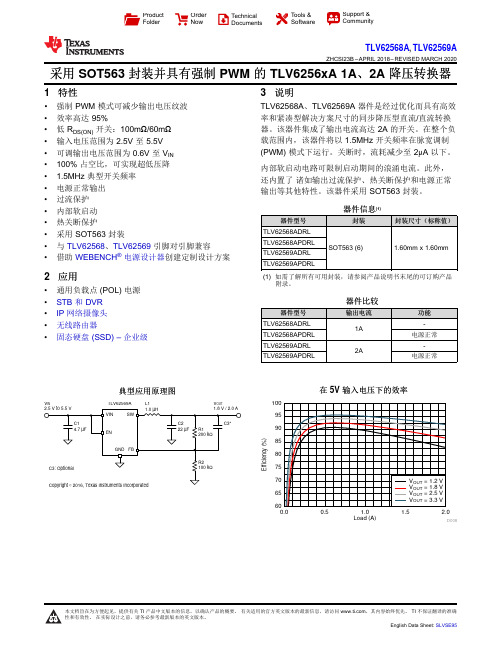
Load (A)E f f i c i e n c y (%)0.00.51.0 1.52.06065707580859095100D008V INV OUTL1TLV62569AProduct Folder Order Now Technical Documents Tools &SoftwareSupport &CommunityTLV62568A ,TLV62569AZHCSI23B –APRIL 2018–REVISED MARCH 2020采用SOT563封装并具有强制PWM 的TLV6256xA 1A 、2A 降压转换器1特性•强制PWM 模式可减少输出电压纹波•效率高达95%•低R DS(ON)开关:100m Ω/60m Ω•输入电压范围为2.5V 至5.5V •可调输出电压范围为0.6V 至V IN •100%占空比,可实现超低压降• 1.5MHz 典型开关频率•电源正常输出•过流保护•内部软启动•热关断保护•采用SOT563封装•与TLV62568、TLV62569引脚对引脚兼容•借助WEBENCH ®电源设计器创建定制设计方案2应用•通用负载点(POL)电源•STB 和DVR •IP 网络摄像头•无线路由器•固态硬盘(SSD)–企业级3说明TLV62568A 、TLV62569A 器件是经过优化而具有高效率和紧凑型解决方案尺寸的同步降压型直流/直流转换器。
该器件集成了输出电流高达2A 的开关。
在整个负载范围内,该器件将以1.5MHz 开关频率在脉宽调制(PWM)模式下运行。
关断时,流耗减少至2μA 以下。
内部软启动电路可限制启动期间的浪涌电流。
此外,还内置了诸如输出过流保护、热关断保护和电源正常输出等其他特性。
该器件采用SOT563封装。
器件信息(1)器件型号封装封装尺寸(标称值)TLV62568ADRL SOT563(6)1.60mm x 1.60mmTLV62568APDRL TLV62569ADRL TLV62569APDRL(1)如需了解所有可用封装,请参阅产品说明书末尾的可订购产品附录。
德州仪器MAX4372-MAX4372T 电流检测放大器 用户手册说明书

General DescriptionThe MAX4372 low-cost, precision, high-side current-sense amplifier is available in a tiny, space-saving SOT23 5-pin package. Offered in three gain versions (T = 20V/V, F = 50V/V, and H = 100V/V), this device oper-ates from a single 2.7V to 28V supply and consumes only 30μA. It features a voltage output that eliminates the need for gain-setting resistors and is ideal for today’s notebook computers, cell phones, and other systems where battery/ DC current monitoring is critical.High-side current monitoring is especially useful in bat-tery-powered systems since it does not interfere with the ground path of the battery charger. The input common-mode range of 0 to 28V is independent of the supply volt-age and ensures that the current-sense feedback remains viable even when connected to a 2-cell battery pack in deep discharge.The user can set the full-scale current reading by choos-ing the device (T, F, or H) with the desired voltage gain and selecting the appropriate external sense resistor. This capability offers a high level of integration and flex-ibility, resulting in a simple and compact current-sense solution. For higher bandwidth applications, refer to the MAX4173T/F/H data sheet.Applications●Power-Management Systems●General-System/Board-Level Current Monitoring●Notebook Computers●Portable/Battery-Powered Systems●Smart-Battery Packs/Chargers●Cell Phones●Precision-Current Sources Features●Low-Cost, Compact Current-Sense Solution●30μA Supply Current● 2.7V to 28V Operating Supply●0.18% Full-Scale Accuracy●0.3mV Input Offset Voltage●Low 1.5Ω Output Impedance●Three Gain Versions Available• 20V/V (MAX4372T)• 50V/V (MAX4372F)• 100V/V (MAX4372H)●High Accuracy +2V to +28V Common-Mode Range,Functional Down to 0V, Independent of SupplyVoltage●Available in a Space-Saving 5-Pin SOT23 Packageand 3 x 2 UCSP™ (1mm x 1.5mm) Package Ordering Information appears at end of data sheet.UCSP is a trademark of Maxim Integrated Products, Inc.19-1548; Rev 5; 5/11+Denotes lead(Pb)-free/RoHS-compliant package.T = Tape and reel.*Note: Gain values are as follows: 20V/V for the T version,50V/V for the F version, and 100V/V for the H version. Current-Sense Amplifier with Voltage OutputPin ConfigurationsOrdering InformationPARTTEMPRANGEPIN-PACKAGETOPMARK MAX4372T EUK+T-40°C to +85°C 5 SOT23ADIU MAX4372TESA+-40°C to +85°C8 SO—MAX4372TEBT+T-40°C to +85°C 3 x 2 UCSP ACXV CC , RS+, RS- to GND .........................................-0.3V to +30V OUT to GND ..........................................................-0.3V to +15V Differential Input Voltage (V RS+ - V RS-) .............................±0.3V Current into Any Pin .........................................................±10mA Continuous Power Dissipation (T A = +70°C)5-Pin SOT23 (derate 3.9mW/°C above +70°C) .......312.6mW 8-Pin SO (derate 7.4mW/°C above +70°C) ..............588.2mW 3 x 2 UCSP (derate 3.4mW/°C above +70°C) .........273.2mWOperating Temperature Range ...........................-40°C to +85°C Storage Temperature Range ............................-65°C to +150°C Lead Temperature (soldering, 10s) .................................+300°C Soldering Temperature (reflow) .......................................+260°C(V RS+ = 0 to 28V, V CC = 2.7V to 28V, V SENSE = 0V, R LOAD = 1MΩ, T A = T MIN to T MAX , unless otherwise noted. Typical values are at T A = +25°C.) (Note 1)Current-Sense Amplifier with Voltage OutputAbsolute Maximum RatingsStresses beyond those listed under “Absolute Maximum Ratings” may cause permanent damage to the device. These are stress ratings only, and functional operation of the device at these or any other conditions beyond those indicated in the operational sections of the specifications is not implied. Exposure to absolute maximum rating conditions for extended periods may affect device reliability.Electrical CharacteristicsPARAMETERSYMBOL CONDITIONSMIN TYPMAX UNITS Operating Voltage Range (Note 2)V CC 2.728V Common-Mode Input Range (Note 3)V CMR 028V Common-Mode Rejection CMR V RS+ > 2V85dB Supply Current I CC V RS+ > 2V, V SENSE = 5mV 3060μA Leakage CurrentI RS+, I RS-V CC = 0V, V RS+ = 28V 0.051.2μAInput Bias CurrentI RS+V RS+ > 2V 01μAV RS+ ≤ 2V -25+2I RS-V RS+ > 2V 02V RS+ ≤ 2V-50+2Full-Scale Sense Voltage (Note 4)V SENSEGain = 20V/V or 50V/V 150mV Gain = 100V/V 100Input Offset Voltage (Note 5)V OST A = +25°CV CC = V RS+ = 12V MAX4372_ESA 0.3±0.8mVMAX4372_EUK, _EBT 0.3±1.3T A = T MIN to T MAX V CC = V RS+ = 12VMAX4372_ESA ±1.1MAX4372_EUK, _EBT±1.9Full-Scale Accuracy (Note 5)V SENSE = 100mV, V CC = 12V,V RS+ = 12V, T A = +25°C (Note 7)±0.18±3%Total OUT Voltage Error (Note 6)V SENSE = 100mV, V CC = 12V,V RS+ = 12V (Note 7)±6V SENSE = 100mV, V CC = 28V,V RS+ = 28V (Note 7)±0.15±7V SENSE = 100mV, V CC = 12V,V RS+ = 0.1V (Note 7)±1±28V SENSE = 6.25mV, V CC = 12V,V RS+ = 12V (Note 8)±0.15(V RS+ = 0 to 28V, V CC = 2.7V to 28V, V SENSE = 0V, R LOAD = 1MΩ, T A = T MIN to T MAX , unless otherwise noted. Typical values are at T A = +25°C.) (Note 1)Note 1: All devices are 100% production tested at T A = +25°C. All temperature limits are guaranteed by design.Note 2: Guaranteed by PSR test.Note 3: Guaranteed by OUT voltage error test.Note 4: Output voltage is internally clamped not to exceed 12V.Note 5: V OS is extrapolated from the gain accuracy tests.Note 6: Total OUT voltage error is the sum of gain and offset voltage errors.Note 7: Measured at I OUT = -500μA (R LOAD = 4kΩ for gain = 20V/V, R LOAD = 10kΩ for gain = 50V/V, R LOAD = 20kΩ for gain = 100V/V).Note 8: 6.25mV = 1/16 of 100mV full-scale voltage (C/16).Note 9: The device does not reverse phase when overdriven.Current-Sense Amplifier with Voltage OutputElectrical Characteristics (continued)PARAMETERSYMBOL CONDITIONSMINTYP MAXUNITSOUT Low Voltage(MAX4372T, MAX4372F)V OLV CC = 2.7V,V SENSE = -10mV, V RS+ = 28V I OUT = 10μA 2.6mVI OUT = 100μA 965OUT Low Voltage (MAX4372H)V OLV CC = 2.7V,V SENSE = -10mV, V RS+ = 12VI OUT = 10μA 2.6mVI OUT = 100μA965OUT High VoltageV CC - V OHV CC = 2.7V, I OUT = -500μA, V SENSE = 250mV, V RS+ = 28V0.10.25V-3dB Bandwidth BWV RS+ = 12V,V CC = 12V,C LOAD = 10pFV SENSE = 20mV,gain = 20V/V275kHzV SENSE = 20mV,gain = 50V/V 200V SENSE = 20mV,gain = 100V/V 110V SENSE = 6.25mV50GainMAX4372T20V/VMAX4372F 50MAX4372H100Gain AccuracyV SENSE = 20mV to 100mV, V R S + = 12V T A = +25°C ±0.25±2.5%T A = -40°C to +85°C ±5.5OUT Settling Time to 1% of Final ValueGain = 20V/V, V CC = 12V, V RS+ = 12V, C LOAD = 10pFV SENSE = 6.25mV to 100mV20µsV SENSE = 100mV to 6.25mV20Capacitive-Load Stability No sustained oscillations1000pF OUT Output Resistance R OUT V SENSE = 100mV 1.5ΩPower-Supply Rejection PSRV OUT = 2V, V RS+ > 2V7585dB Power-Up Time to 1% of Final ValueV CC = 12V, V RS+ = 12V,V SENSE = 100mV, C LOAD = 10pF 0.5ms Saturation Recovery Time (Note 9)V CC = 12V, V RS+ = 12V, C LOAD = 10pF0.1ms(V CC = 12V, V RS+ = 12V, V SENSE = 100mV, T A = +25°C, unless otherwise noted.)Current-Sense Amplifier with Voltage OutputTypical Operating Characteristics25.027.530.032.535.0SUPPLY CURRENT vs. SUPPLY VOLTAGESUPPLY VOLTAGE (V)S U P P L Y C U R R E N T (µA )121648202428-1.2-0.8-1.0-0.2-0.4-0.60.40.200.6010515202530TOTAL OUTPUT ERROR vs. SUPPLY VOLTAGESUPPLY VOLTAGE (V)O U T P U T E R R O R (%)00.20.40.60.81.01.21.41.610515202530TOTAL OUTPUT ERROR vs. COMMON-MODE VOLTAGECOMMON-MODE VOLTAGE (V)O U T P U T E R R O R (%)510152025303540-401060-153585SUPPLY CURRENT vs. TEMPERATURETEMPERATURE (°C)S U P P L Y C U R R E N T (µA )-1.0-0.50.501.01.5010050150200250300TOTAL OUTPUT ERROR vs. V SENSEV SENSE (mV)O U T P U T E R R O R (%)-1.0-0.9-0.8-0.7-0.6-0.5-0.4-0.3-0.2-0.10GAIN ACCURACY vs. TEMPERATURETEMPERATURE (°C)G A I N A C C U R A C Y (%)-401060-15358528.029.028.530.029.531.531.030.532.0SUPPLY CURRENTvs. COMMON-MODE VOLTAGECOMMON-MODE VOLTAGE (V)S U P P L Y C U R R E N T (µA )-45-90100100k10k 1k POWER-SUPPLY REJECTIONvs. FREQUENCY-75-85-55-65-40-70-80-50-60M A X 4372T t o c 06FREQUENCY (Hz)P S R (d B )-1.0-0.8-0.6-0.4-0.200.20.40.60.81.0-401060-153585TOTAL OUTPUT ERROR vs. TEMPERATURETEMPERATURE (°C)T O T A L O U T P U T E R R O R (%)(V CC = 12V, V RS+ = 12V, V SENSE = 100mV, T A = +25°C, unless otherwise noted.)Current-Sense Amplifier with Voltage OutputTypical Operating Characteristics (continued)V OUTV SENSE600mV200mV30mV10mV MAX4372TSMALL-SIGNAL TRANSIENT RESPONSEMAX4372T toc1020µs/div V OUTV SENSE1V3V50mV 150mV MAX4372TLARGE-SIGNAL TRANSIENT RESPONSEMAX4372T toc1320µs/divV OUTV SENSE 010V0100mV MAX4372HLARGE-SIGNAL TRANSIENT RESPONSE20µs/divMAX4372T toc15V OUTV SENSE2.5V7.5V50mV 150mVMAX4372FLARGE-SIGNAL TRANSIENT RESPONSE20µs/divMAX4372T toc143-81k100k10k1MSMALL-SIGNAL GAIN vs. FREQUENCY-7FREQUENCY (Hz)G A I N (d B)-6-5-4-3-2-1012V OUTV SENSE 1.5V0.5V30mV 10mVMAX4372FSMALL-SIGNAL TRANSIENT RESPONSEMAX4372T toc1120µs/div V OUTV SENSE 3V1V30mV10mV MAX4372HSMALL-SIGNAL TRANSIENT RESPONSEMAX4372T toc1220µs/divDetailed DescriptionThe MAX4372 high-side current-sense amplifier features a 0 to 28V input common-mode range that is indepen-dent of supply voltage. This feature allows the monitoring of current flow out of a battery in deep discharge, and also enables high-side current sensing at voltages far in excess of the supply voltage (V CC).Current flows through the sense resistor, generating a sense voltage (Figure 1. Functional Diagram). Since A1’s inverting input is high impedance, the voltage on the negative terminal equals V IN - V SENSE. A1 forces its positive terminal to match its negative terminal; therefore, the voltage across R G1 (V IN - V1-) equals V SENSE. This creates a current to flow through R G1 equal to V SENSE/ R G1. The transistor and current mirror amplify the current by a factor of β. This makes the current flowing out of the current mirror equal to:I M = β V SENSE/R G1A2’s positive terminal presents high impedance, so this current flows through R GD, with the following result:V2+ = R GD β x V SENSE/R G1R1 and R2 set the closed-loop gain for A2, which ampli-fies V2+, yielding:V OUT = R GD x β x V SENSE/R G1 (1 + R2/R1)The gain of the device equals:OUT SEN G1SE RGD x (1 + R2/R1)V V/Rβ=Applications Information Recommended Component ValuesThe MAX4372 operates over a wide variety of current ranges with different sense resistors. Table 1 lists com-mon resistor values for typical operation of the MAX4372.Choosing R SENSEGiven the gain and maximum load current, select R SENSE such that V OUT does not exceed V CC - 0.25V or 10V. To measure lower currents more accurately, use a high value for R SENSE. A higher value develops a higher sense volt-age, which overcomes offset voltage errors of the internal current amplifier.In applications monitoring very high current, ensure R SENSE is able to dissipate its own I2R losses. If the resistor’s rated power dissipation is exceeded, its value may drift or it may fail altogether, causing a differential voltage across the terminals in excess of the absolute maximum ratings.Figure 1. Functional DiagramCurrent-Sense Amplifier with Voltage OutputPin/Bump DescriptionPIN BUMPNAME FUNCTIONSOT23SO UCSP13A2GND Ground24A3OUT Output Voltage. V OUT is proportional to the magnitude of V SENSE (V RS+ - V RS-).31A1V CC Supply Voltage. Use at least a 0.1μF capacitor to decouple V CC from fast transients.48B1RS+Power Connection to the External Sense Resistor56B3RS-Load-Side Connection to the External Sense Resistor —2, 5, 7—N.C.No Connection. Not internally connected.Using a PC Board Trace as R SENSEIf the cost of R SENSE is an issue and accuracy is not criti-cal, use the alternative solution shown in Figure 2. This solution uses copper PC board traces to create a sense resistor. The resistivity of a 0.1in wide trace of 2oz copper is about 30mΩ/ft. The resistance temperature coefficient of copper is fairly high (approximately 0.4%/°C), so sys-tems that experience a wide temperature variance must compensate for this effect. In addition, self-heating intro-duces a nonlinearity error. Do not exceed the maximum power dissipation of the copper trace.For example, the MAX4372T (with a maximum load cur-rent of 10A and an R SENSE of 5mΩ) creates a full-scale V SENSE of 50mV that yields a maximum V OUT of 1V. R SENSE, in this case, requires about 2in of 0.1in wide copper trace.UCSP Applications InformationFor the latest application details on UCSP construction, dimensions, tape carrier information, printed circuit board techniques, bump-pad layout, and recommended reflow temperature profile, as well as the latest information on reliability testing results, go to the Maxim’s website at /ucsp to find the Application Note: UCSP—A Wafer-Level Chip-Scale Package.Figure 2. Connections Showing Use of PC BoardTable 1. Recommended Component ValuesCurrent-Sense Amplifier with Voltage OutputFULL-SCALE LOAD CURRENT,I LOAD (A)CURRENT-SENSERESISTOR,R SENSE (mΩ)GAIN(V/V)FULL-SCALE OUTPUTVOLTAGE (FULL-SCALEV SENSE = 100mV),V OUT (V)0.1100020 2.0 50 5.0 10010.0110020 2.0 50 5.0 10010.052020 2.0 50 5.0 10010.0101020 2.0 50 5.0 10010.0Current-Sense Amplifier with Voltage Output Ordering Information (continued)Pin Configurations (continued)PARTTEMPRANGEPIN-PACKAGETOPMARKMAX4372F EUK+T-40°C to +85°C 5 SOT23ADIV MAX4372FESA+-40°C to +85°C8 SO—MAX4372FEBT+T-40°C to +85°C 3 x 2 UCSP ACX MAX4372H EUK+T-40°C to +85°C 5 SOT23ADIW MAX4372HESA+-40°C to +85°C8 SO—MAX4372HEBT+T-40°C to +85°C 3 x 2 UCSP ACZChip InformationPROCESS: BiCMOS+Denotes lead(Pb)-free/RoHS-compliant package. T = Tape and reel.Current-Sense Amplifier with Voltage Output Package InformationFor the latest package outline information and land patterns (footprints), go to /packages. Note that a “+”, “#”, or “-” in the package code indicates RoHS status only. Package drawings may show a different suffix character, but the drawing pertains to the package regardless of RoHS status.PACKAGE TYPE PACKAGE CODE OUTLINE ND PATTERN NO.5 SOT23U5+121-005790-01748 SO S8+221-004190-00965 UCSP B6+221-0097—Note: MAX4372_EBT uses package code B6-2.Current-Sense Amplifier with Voltage Output Package Information (continued)For the latest package outline information and land patterns (footprints), go to /packages. Note that a “+”, “#”, or “-” in the package code indicates RoHS status only. Package drawings may show a different suffix character, but the drawing pertains to the package regardless of RoHS status.Current-Sense Amplifier with Voltage Output Package Information (continued)For the latest package outline information and land patterns (footprints), go to /packages. Note that a “+”, “#”, or “-” in the package code indicates RoHS status only. Package drawings may show a different suffix character, but the drawing pertains to the package regardless of RoHS status. Maxim Integrated │11Maxim Integrated cannot assume responsibility for use of any circuitry other than circuitry entirely embodied in a Maxim Integrated product. No circuit patent licenses are implied. Maxim Integrated reserves the right to change the circuitry and specifications without notice at any time. The parametric values (min and max limits) shown in the Electrical Characteristics table are guaranteed. Other parametric values quoted in this data sheet are provided for guidance.Maxim Integrated and the Maxim Integrated logo are trademarks of Maxim Integrated Products, Inc.Current-Sense Amplifier with Voltage Output© 2011 Maxim Integrated Products, Inc. │ 12Revision HistoryREVISIONNUMBERREVISION DATE DESCRIPTION PAGES CHANGED 47/09Updated feature in accordance with actual performance of the product 155/11Updated V RST conditions to synchronize with tested material and addedlead-free designation 1–3, 8For pricing, delivery, and ordering information, please contact Maxim Direct at 1-888-629-4642, or visit Maxim Integrated’s website at .。
- 1、下载文档前请自行甄别文档内容的完整性,平台不提供额外的编辑、内容补充、找答案等附加服务。
- 2、"仅部分预览"的文档,不可在线预览部分如存在完整性等问题,可反馈申请退款(可完整预览的文档不适用该条件!)。
- 3、如文档侵犯您的权益,请联系客服反馈,我们会尽快为您处理(人工客服工作时间:9:00-18:30)。
TI(德州仪器)德州仪器,简称TI,全球约 30,300人,总部位于美国得克萨斯州的达拉斯,2008年营业额为185亿美元, 是全球领先的半导体公司,为现实世界的信号处理提供创新的数字信号处理(DSP)及模拟技术, 应用领域涵盖无线通讯、宽带、网络家电、数字马达控制与消费类市场。
TI(德州仪器)目录更多关于产品•MSP430系列单片机•TMS370系列单片机•TMS470系列单片机•Stellaris系列单片机•32位C2000单片机•C2000 DSP•C5000 DSP•C6000 DSP•达芬奇 DSP•A/D转换器•D/A转换器•电池管理•PWM控制器•DC/DC控制器MSP430系列单片机MSP430 系列是一个 16 位的、具有精简指令集的、超低功耗的混合型单片机,在 1996 年问世,由于它具有极低的功耗、丰富的片内外设和方便灵活的开发手段,已成为众多单片机系列中一颗耀眼的新星。
MSP430 系列单片机的迅速发展和应用范围的不断扩大,主要取决于以下的特点。
强大的处理能力 MSP430 系列单片机是一个 16 位的单片机,采用了精简指令集( RISC )结构,具有丰富的寻址方式( 7 种源操作数寻址、 4 种目的操作数寻址)、简洁的 27 条内核指令以及大量的模拟指令;大量的寄存器以及片内数据存储器都可参加多种运算;还有高效的查表处理指令;有较高的处理速度,在 8MHz 晶体驱动下指令周期为 125 ns 。
这些特点保证了可编制出高效率的源程序。
在运算速度方面, MSP430 系列单片机能在 8MHz 晶体的驱动下,实现 125ns 的指令周期。
16 位的数据宽度、 125ns 的指令周期以及多功能的硬件乘法器(能实现乘加)相配合,能实现数字信号处理的某些算法(如 FFT 等)。
MSP430 系列单片机的中断源较多,并且可以任意嵌套,使用时灵活方便。
当系统处于省电的备用状态时,用中断请求将它唤醒只用 6us 。
超低功耗 MSP430 单片机之所以有超低的功耗,是因为其在降低芯片的电源电压及灵活而可控的运行时钟方面都有其独到之处。
MSP430 系列单片机最新报价产品型号产品描述价格($) MSP430F2001IPWR IC MCU 16BIT 1K FLASH 14-TSSOP 0.472 MSP430F2001IPWR IC MCU 16BIT 1K FLASH 14-TSSOP 0.963 MSP430F2001IPWR IC MCU 16BIT 1K FLASH 14-TSSOP 1.242 MSP430F2001TPWR IC MCU 16BIT 1K FLASH 14-TSSOP 0.527 MSP430F2001TPWR IC MCU 16BIT 1K FLASH 14-TSSOP 1.177 MSP430F2001TPWR IC MCU 16BIT 1K FLASH 14-TSSOP 1.293 MSP430F2011IPWR IC MCU 16BIT 2K FLASH 14-TSSOP 0.486 MSP430F2011IPWR IC MCU 16BIT 2K FLASH 14-TSSOP 1.176 MSP430F2011IPWR IC MCU 16BIT 2K FLASH 14-TSSOP 1.281 MSP430F2002IPWR IC MCU 16BIT 1K FLASH 14-TSSOP 0.548 MSP430F2002IPWR IC MCU 16BIT 1K FLASH 14-TSSOP 1.348 MSP430F2002IPWR IC MCU 16BIT 1K FLASH 14-TSSOP 1.813 MSP430F2101TPWR IC MCU 16BIT 1K FLASH 20-TSSOP 0.586 MSP430F2101TPWR IC MCU 16BIT 1K FLASH 20-TSSOP 1.813 MSP430F2101TPWR IC MCU 16BIT 1K FLASH 20-TSSOP 1.568 MSP430F2111IPWR IC MCU 16BIT 2K FLASH 20-TSSOP 0.68 MSP430F2111IPWR IC MCU 16BIT 2K FLASH 20-TSSOP 1.764 MSP430F2111IPWR IC MCU 16BIT 2K FLASH 20-TSSOP 1.715 MSP430F2111TDGVR IC MCU 16BIT 2K FLASH 20-TVSOP 0.767 MSP430F2111TDGVR IC MCU 16BIT 2K FLASH 20-TVSOP 1.792 MSP430F2111TDGVR IC MCU 16BIT 2K FLASH 20-TVSOP 1.904 MSP430F2001IRSAT IC MCU 16BIT 1K FLASH 16-QFN 0.737 MSP430F2001IRSAT IC MCU 16BIT 1K FLASH 16-QFN 1.235 MSP430F2001IRSAT IC MCU 16BIT 1K FLASH 16-QFN 1.158 MSP430F2121IPWR IC MCU 16BIT 4K FLASH 20-TSSOP 0.778 MSP430F2121IPWR IC MCU 16BIT 4K FLASH 20-TSSOP 2.173 MSP430F2121IPWR IC MCU 16BIT 4K FLASH 20-TSSOP 2.048 MSP430F2012IPWR IC MCU 16BIT 2K FLASH 14-TSSOP 0.838 MSP430F2012IPWR IC MCU 16BIT 2K FLASH 14-TSSOP 1.764 MSP430F2012IPWR IC MCU 16BIT 2K FLASH 14-TSSOP 2.079 MSP430F2012TPWR IC MCU 16BIT 2K FLASH 14-TSSOP 0.949 MSP430F2012TPWR IC MCU 16BIT 2K FLASH 14-TSSOP 2.221 MSP430F2012TPWR IC MCU 16BIT 2K FLASH 14-TSSOP 2.568 MSP430F2112IRHBR IC MCU 16BIT 2K FLASH 32-QFN 0.878 MSP430F2112IRHBR IC MCU 16BIT 2K FLASH 32-QFN 2.244 MSP430F2112IRHBR IC MCU 16BIT 2K FLASH 32-QFN 1.881 MSP430F2013IPWR IC MCU 16BIT 2K FLASH 14-TSSOP 0.926 MSP430F2013IPWR IC MCU 16BIT 2K FLASH 14-TSSOP 2.592 MSP430F2013IPWR IC MCU 16BIT 2K FLASH 14-TSSOP 2.484 MSP430F2131IPWR IC MCU 16BIT 8K FLASH 20-TSSOP 1.117 MSP430F2131IPWR IC MCU 16BIT 8K FLASH 20-TSSOP 2.484 MSP430F2131IPWR IC MCU 16BIT 8K FLASH 20-TSSOP 2.412MSP430F2131IDWR IC MCU 16BIT 8K FLASH 20-SOIC 2.592 MSP430F2131IDWR IC MCU 16BIT 8K FLASH 20-SOIC 2.664 MSP430F2013TPWR IC MCU 16BIT 2K FLASH 14-TSSOP 1.059 MSP430F2013TPWR IC MCU 16BIT 2K FLASH 14-TSSOP 2.47 MSP430F2013TPWR IC MCU 16BIT 2K FLASH 14-TSSOP 2.552 MSP430F2122IRHBR IC MCU 16BIT 4K FLASH 32-QFN 1.061 MSP430F2122IRHBR IC MCU 16BIT 4K FLASH 32-QFN 3.108 MSP430F2122IRHBR IC MCU 16BIT 4K FLASH 32-QFN 2.73 MSP430F1121AIPWR IC MCU 16BIT 4KB FLASH 20-TSSOP 1.322 MSP430F1121AIPWR IC MCU 16BIT 4KB FLASH 20-TSSOP 2.394 MSP430F1121AIPWR IC MCU 16BIT 4KB FLASH 20-TSSOP 2.646 MSP430F2121IRGET IC MCU 16BIT 4K FLASH 24-QFN 1.121 MSP430F2121IRGET IC MCU 16BIT 4K FLASH 24-QFN 2.298 MSP430F2121IRGET IC MCU 16BIT 4K FLASH 24-QFN 2.464 MSP430F2132IRHBR IC MCU 16BIT 8K FLASH 32-QFN 1.476 MSP430F2132IRHBR IC MCU 16BIT 8K FLASH 32-QFN 2.79 MSP430F2132IRHBR IC MCU 16BIT 8K FLASH 32-QFN 2.925 MSP430F2132IPWR IC MCU 16BIT 8K FLASH 28-TSSOP 1.317 MSP430F2132IPWR IC MCU 16BIT 8K FLASH 28-TSSOP 2.835 MSP430F2132IPWR IC MCU 16BIT 8K FLASH 28-TSSOP 3.285 MSP430F2101IDWR IC MCU 16BIT 1K FLASH 20-SOIC 0.599 MSP430F2101IDWR IC MCU 16BIT 1K FLASH 20-SOIC 1.533 MSP430F2101IDWR IC MCU 16BIT 1K FLASH 20-SOIC 1.554 MSP430F2132TPWR IC MCU 16BIT 8K FLASH 28-TSSOP 1.339 MSP430F2132TPWR IC MCU 16BIT 8K FLASH 28-TSSOP 3.218 MSP430F2132TPWR IC MCU 16BIT 8K FLASH 28-TSSOP 3.663 MSP430F2232IDAR IC MCU 16BIT 8K FLASH 38-TSSOP 1.405 MSP430F2232IDAR IC MCU 16BIT 8K FLASH 38-TSSOP 3.663 MSP430F2232IDAR IC MCU 16BIT 8K FLASH 38-TSSOP 3.415 MSP430F2011TPWR IC MCU 16BIT 2K FLASH 14-TSSOP 0.548 MSP430F2011TPWR IC MCU 16BIT 2K FLASH 14-TSSOP 1.715 MSP430F2011TPWR IC MCU 16BIT 2K FLASH 14-TSSOP 1.544 MSP430F2101TDGVR IC MCU 16BIT 1K FLASH 20-TVSOP 0.548 MSP430F2101TDGVR IC MCU 16BIT 1K FLASH 20-TVSOP 1.495 MSP430F2101TDGVR IC MCU 16BIT 1K FLASH 20-TVSOP 1.348 MSP430F2111IDWR IC MCU 16BIT 2K FLASH 20-SOIC 0.567 MSP430F2111IDWR IC MCU 16BIT 2K FLASH 20-SOIC 1.69 MSP430F2111IDWR IC MCU 16BIT 2K FLASH 20-SOIC 1.348 MSP430F415IPMR IC MCU 16BIT 16K FLASH 64-LQFP 1.562 MSP430F415IPMR IC MCU 16BIT 16K FLASH 64-LQFP 3.024 MSP430F415IPMR IC MCU 16BIT 16K FLASH 64-LQFP 3.51 MSP430F1132IPWR IC MCU 16BIT 8KB FLASH 20-TSSOP 1.915MSP430F1132IPWR IC MCU 16BIT 8KB FLASH 20-TSSOP 3.42 MSP430F1232IRHBR IC MCU 16BIT 8KB FLASH 32-VQFN 1.691 MSP430F1232IRHBR IC MCU 16BIT 8KB FLASH 32-VQFN 4.305 MSP430F1232IRHBR IC MCU 16BIT 8KB FLASH 32-VQFN 3.875 MSP430F2121IDGV IC MCU 16BIT 4K FLASH 20-TVSOP 1.814 MSP430F2111TDWR IC MCU 16BIT 2K FLASH 20-SOIC 0.788 MSP430F2111TDWR IC MCU 16BIT 2K FLASH 20-SOIC 1.876 MSP430F2111TDWR IC MCU 16BIT 2K FLASH 20-SOIC 2.044 MSP430F2111TPWR IC MCU 16BIT 2K FLASH 20-TSSOP 0.799 MSP430F2111TPWR IC MCU 16BIT 2K FLASH 20-TSSOP 1.932 MSP430F2111TPWR IC MCU 16BIT 2K FLASH 20-TSSOP 1.82 MSP430F2272IDAR IC MCU 16BIT 32K FLASH 38-TSSOP 1.726 MSP430F2272IDAR IC MCU 16BIT 32K FLASH 38-TSSOP 4.62 MSP430F2272IDAR IC MCU 16BIT 32K FLASH 38-TSSOP 4.026 MSP430F1101AIPW IC MCU 16BIT 1KB FLASH 20-TSSOP 1.858 MSP430F2232IRHAT IC MCU 16BIT 8K FLASH 40-QFN 2.139 MSP430F2232IRHAT IC MCU 16BIT 8K FLASH 40-QFN 3.57 MSP430F2232IRHAT IC MCU 16BIT 8K FLASH 40-QFN 3.621 MSP430F2012TRSAT IC MCU 16BIT 2K FLASH 16-VQFN 1.204 MSP430F2012TRSAT IC MCU 16BIT 2K FLASH 16-VQFN 2.079 MSP430F2012TRSAT IC MCU 16BIT 2K FLASH 16-VQFN 2.11 MSP430F2274IDAR IC MCU 16BIT 32K FLASH 38-TSSOP 2.021 MSP430F2274IDAR IC MCU 16BIT 32K FLASH 38-TSSOP 4.851 MSP430F2274IDAR IC MCU 16BIT 32K FLASH 38-TSSOP 4.263 MSP430F2003IPWR IC MCU 16BIT 1K FLASH 14-TSSOP 0.936 MSP430F2003IPWR IC MCU 16BIT 1K FLASH 14-TSSOP 2.211 MSP430F2003IPWR IC MCU 16BIT 1K FLASH 14-TSSOP 2.376 MSP430F2112IPWR IC MCU 16BIT 2K FLASH 28-TSSOP 0.878 MSP430F2112IPWR IC MCU 16BIT 2K FLASH 28-TSSOP 2.409 MSP430F2112IPWR IC MCU 16BIT 2K FLASH 28-TSSOP 2.409 MSP430F2121TRGET IC MCU 16BIT 4K FLASH 24-QFN 1.406 MSP430F2121TRGET IC MCU 16BIT 4K FLASH 24-QFN 1.965 MSP430F2121TRGET IC MCU 16BIT 4K FLASH 24-QFN 2.431 MSP430F233TPMR IC MCU 16BIT 8K FLASH 64-LQFP 1.848 MSP430F233TPMR IC MCU 16BIT 8K FLASH 64-LQFP 5.328 MSP430F233TPMR IC MCU 16BIT 8K FLASH 64-LQFP 4.464 MSP430F2013IN IC MCU 16BIT 2K FLASH 14-DIP 2.352 MSP430F2131IDGV IC MCU 16BIT 8K FLASH 20-TVSOP 2.117 MSP430F1111AIRGET IC MCU 16BIT 2KB FLASH 24-QFN 1.319 MSP430F1111AIRGET IC MCU 16BIT 2KB FLASH 24-QFN 2.208 MSP430F1111AIRGET IC MCU 16BIT 2KB FLASH 24-QFN 2.312 MSP430F2003IRSAT IC MCU 16BIT 1K FLASH 16-QFN 1.319MSP430F2003IRSAT IC MCU 16BIT 1K FLASH 16-QFN 2.415 MSP430F2003IRSAT IC MCU 16BIT 1K FLASH 16-QFN 2.45 MSP430F2121TDGVR IC MCU 16BIT 4K FLASH 20-TVSOP 0.949 MSP430F2121TDGVR IC MCU 16BIT 4K FLASH 20-TVSOP 2.429 MSP430F2121TDGVR IC MCU 16BIT 4K FLASH 20-TVSOP 2.221 MSP430F2121TDWR IC MCU 16BIT 4K FLASH 20-SOIC 0.789 MSP430F2121TDWR IC MCU 16BIT 4K FLASH 20-SOIC 2.082 MSP430F2121TDWR IC MCU 16BIT 4K FLASH 20-SOIC 2.533 MSP430F2121TPWR IC MCU 16BIT 4K FLASH 20-TSSOP 0.976 MSP430F2121TPWR IC MCU 16BIT 4K FLASH 20-TSSOP 1.943 MSP430F2121TPWR IC MCU 16BIT 4K FLASH 20-TSSOP 1.978 MSP430F235TPMR IC MCU 16BIT 16KB FLASH 64-LQFP 2.036 MSP430F235TPMR IC MCU 16BIT 16KB FLASH 64-LQFP 5.03 MSP430F235TPMR IC MCU 16BIT 16KB FLASH 64-LQFP 4.547 MSP430F2274TDAR IC MCU 16BIT 32K FLASH 38-TSSOP 2.492 MSP430F2274TDAR IC MCU 16BIT 32K FLASH 38-TSSOP 5.012 MSP430F2274TDAR IC MCU 16BIT 32K FLASH 38-TSSOP 4.081 MSP430F2234IRHAT IC MCU 16BIT 8K FLASH 40-QFN 2.214 MSP430F2234IRHAT IC MCU 16BIT 8K FLASH 40-QFN 3.99 MSP430F2234IRHAT IC MCU 16BIT 8K FLASH 40-QFN 3.192 MSP430F2112TRHBR IC MCU 16BIT 2K FLASH 32-QFN 1.031 MSP430F2112TRHBR IC MCU 16BIT 2K FLASH 32-QFN 2.137 MSP430F2112TRHBR IC MCU 16BIT 2K FLASH 32-QFN 2.288 MSP430F2003TPWR IC MCU 16BIT 1K FLASH 14-TSSOP 1.014 MSP430F2003TPWR IC MCU 16BIT 1K FLASH 14-TSSOP 2.738 MSP430F2003TPWR IC MCU 16BIT 1K FLASH 14-TSSOP 2.362 MSP430F2112TPWR IC MCU 16BIT 2K FLASH 28-TSSOP 0.931 MSP430F2112TPWR IC MCU 16BIT 2K FLASH 28-TSSOP 2.1 MSP430F2112TPWR IC MCU 16BIT 2K FLASH 28-TSSOP 2.175 MSP430F2013TPW IC MCU 16BIT 2K FLASH 14-TSSOP 2.306 MSP430F2013TN IC MCU 16BIT 2K FLASH 14-DIP 2.079 MSP430F427AIPMR IC MCU 16BIT 32KB FLASH 64LQFP 2.388 MSP430F427AIPMR IC MCU 16BIT 32KB FLASH 64LQFP 5.075 MSP430F427AIPMR IC MCU 16BIT 32KB FLASH 64LQFP 4.845 MSP430F1121AIDW IC MCU 16BIT 4KB FLASH 20-SOIC 2.744 MSP430F1121AIDGV IC MCU 16BIT 4KB FLASH 20-TVSOP 2.744 MSP430F1121IDW IC MCU 16BIT 4KB FLASH 20-SOIC 2.156 MSP430F1121IPW IC MCU 16BIT 4KB FLASH 20-TSSOP 2.744 MSP430F2122IPW IC MCU 16BIT 4K FLASH 28-TSSOP 2.666 MSP430F2131TDWR IC MCU 16BIT 8K FLASH 20-SOIC 1.185 MSP430F2131TDWR IC MCU 16BIT 8K FLASH 20-SOIC 2.592 MSP430F2131TDWR IC MCU 16BIT 8K FLASH 20-SOIC 2.875 MSP430F2131TDGVR IC MCU 16BIT 8K FLASH 20-TVSOP 1.077MSP430F2131TDGVR IC MCU 16BIT 8K FLASH 20-TVSOP 2.552 MSP430F2131TPWR IC MCU 16BIT 8K FLASH 20-TSSOP 1.059 MSP430F2131TPWR IC MCU 16BIT 8K FLASH 20-TSSOP 2.308 MSP430F2131TPWR IC MCU 16BIT 8K FLASH 20-TSSOP 2.835 MSP430F2370IRHAT IC MCU 16BIT 32K FLASH 40-QFN 2.808 MSP430F2370IRHAT IC MCU 16BIT 32K FLASH 40-QFN 4.092 MSP430F2471TRGCR IC MCU 16BIT 32K FLASH 64-VQFN 2.334 MSP430F2471TRGCR IC MCU 16BIT 32K FLASH 64-VQFN 4.759 MSP430F2471TRGCR IC MCU 16BIT 32K FLASH 64-VQFN 5.428 MSP430F4250IDLR IC MCU 16BIT 16K FLASH 48-SSOP 3.047 MSP430F4250IDLR IC MCU 16BIT 16K FLASH 48-SSOP 5.737 MSP430F4250IDLR IC MCU 16BIT 16K FLASH 48-SSOP 4.848 MSP430F2272IRHAT IC MCU 16BIT 32KB FLASH 40-QFN 3.081 MSP430F2272IRHAT IC MCU 16BIT 32KB FLASH 40-QFN 3.915 MSP430F2272IRHAT IC MCU 16BIT 32KB FLASH 40-QFN 3.713 MSP430FE425IPMR IC MCU 16BIT 16KB FLASH 64-LQFP 3.055 MSP430FE425IPMR IC MCU 16BIT 16KB FLASH 64-LQFP 5.672 MSP430FE425IPMR IC MCU 16BIT 16KB FLASH 64-LQFP 4.932 MSP430F1121AIRGER IC MCU 16BIT 4KB FLASH 20-QFN 1.285 MSP430F1121AIRGER IC MCU 16BIT 4KB FLASH 20-QFN 2.352 MSP430F1121AIRGER IC MCU 16BIT 4KB FLASH 20-QFN 2.478 MSP430F2122IPWR IC MCU 16BIT 4K FLASH 28-TSSOP 1.024 MSP430F2122IPWR IC MCU 16BIT 4K FLASH 28-TSSOP 2.646 MSP430F2122IPWR IC MCU 16BIT 4K FLASH 28-TSSOP 2.814 MSP430F2131TRGET IC MCU 16BIT 8K FLASH 24-QFN 1.865 MSP430F2131TRGET IC MCU 16BIT 8K FLASH 24-QFN 2.814 MSP430F2131TRGET IC MCU 16BIT 8K FLASH 24-QFN 2.352 MSP430F112IPW IC MCU 16BIT 4KB FLASH 20-TSSOP 3.024 MSP430F412IPM IC MCU 16BIT 4K FLASH 64-LQFP 2.647 MSP430F247TRGCR IC MCU 16BIT 32K FLASH 64-VQFN 3.227 MSP430F247TRGCR IC MCU 16BIT 32K FLASH 64-VQFN 5.226 MSP430F247TRGCR IC MCU 16BIT 32K FLASH 64-VQFN 5.226 MSP430F5418IPNR IC MCU 16BIT 128K FLASH 80-LQFP 3.208 MSP430F5418IPNR IC MCU 16BIT 128K FLASH 80-LQFP 6.038 MSP430F5418IPNR IC MCU 16BIT 128K FLASH 80-LQFP 6.475 MSP430F413IPM IC MCU 16BIT 8K FLASH 64-LQFP 2.733 MSP430F2254TRHAT IC MCU 16BIT 16K FLASH 40-QFN 3.173 MSP430F2254TRHAT IC MCU 16BIT 16K FLASH 40-QFN 4.778 MSP430F2254TRHAT IC MCU 16BIT 16K FLASH 40-QFN 4.336 MSP430F247TPMR IC MCU 16BIT 32K FLASH 64-LQFP 2.57 MSP430F247TPMR IC MCU 16BIT 32K FLASH 64-LQFP 5.046 MSP430F247TPMR IC MCU 16BIT 32K FLASH 64-LQFP 5.406MSP430F122IPW IC MCU 16BIT 4KB FLASH 28-TSSOP 3.326 MSP430F1122IDW IC MCU 16BIT 4KB FLASH 20-SOIC 3.373 MSP430F2132TPW IC MCU 16BIT 8K FLASH 28-TSSOP 3.28 MSP430F2122TRHBR IC MCU 16BIT 4K FLASH 32-QFN 1.237 MSP430F2122TRHBR IC MCU 16BIT 4K FLASH 32-QFN 2.65 MSP430F2122TRHBR IC MCU 16BIT 4K FLASH 32-QFN 3.208 MSP430F413IRTDR IC MCU 16BIT 8K FLASH 64-QFN 1.383 MSP430F413IRTDR IC MCU 16BIT 8K FLASH 64-QFN 2.784 MSP430F413IRTDR IC MCU 16BIT 8K FLASH 64-QFN 2.784 MSP430F412IRTDT IC MCU 16BIT 4K FLASH 64-QFN 1.776 MSP430F412IRTDT IC MCU 16BIT 4K FLASH 64-QFN 3.264 MSP430F412IRTDT IC MCU 16BIT 4K FLASH 64-QFN 2.736 MSP430F5419IPZR IC MCU 16BIT 128K FLASH 100-LQFP 3.45 MSP430F5419IPZR IC MCU 16BIT 128K FLASH 100-LQFP 6.962 MSP430F5419IPZR IC MCU 16BIT 128K FLASH 100-LQFP 6.382 MSP430F4270IDLR IC MCU 16BIT 32K FLASH 48-SSOP 3.647 MSP430F4270IDLR IC MCU 16BIT 32K FLASH 48-SSOP 5.995 MSP430F4270IDLR IC MCU 16BIT 32K FLASH 48-SSOP 5.609 MSP430F2132TRHBR IC MCU 16BIT 8K FLASH 32-QFN 1.273 MSP430F2132TRHBR IC MCU 16BIT 8K FLASH 32-QFN 3.267 MSP430F2132TRHBR IC MCU 16BIT 8K FLASH 32-QFN 3.564 MSP430F4132IRGZR IC MCU 16BIT 8K FLASH LP 48QFN 1.624 MSP430F4132IRGZR IC MCU 16BIT 8K FLASH LP 48QFN 3.614 MSP430F4132IRGZR IC MCU 16BIT 8K FLASH LP 48QFN 3.614 MSP430F122IRHBR IC MCU 16BIT 4KB FLASH 32-QFN 1.514 MSP430F122IRHBR IC MCU 16BIT 4KB FLASH 32-QFN 3.317 MSP430F122IRHBR IC MCU 16BIT 4KB FLASH 32-QFN 2.92 MSP430F413IRTDT IC MCU 16BIT 8K FLASH 64-QFN 2.137 MSP430F413IRTDT IC MCU 16BIT 8K FLASH 64-QFN 3.614 MSP430F413IRTDT IC MCU 16BIT 8K FLASH 64-QFN 3.168 MSP430F1222IPW IC MCU 16BIT 4KB FLASH 28-TSSOP 2.873 MSP430F123IPW IC MCU 16BIT 8KB FLASH 28-TSSOP 3.226 MSP430F123IDW IC MCU 16BIT 8KB FLASH 28-SOIC 2.974 MSP430F4152IPM IC MCU 16BIT 16K FLASH 64-LQFP 3.367 MSP430F248TRGCR IC MCU 16BIT 48K FLASH 64-VQFN 3.796 MSP430F248TRGCR IC MCU 16BIT 48K FLASH 64-VQFN 6.89 MSP430F248TRGCR IC MCU 16BIT 48K FLASH 64-QFN 6.254 MSP430F5435IPNR IC MCU 16BIT 192K FLASH 80-LQFP 3.685 MSP430F5435IPNR IC MCU 16BIT 192K FLASH 80-LQFP 7.135 MSP430F5435IPNR IC MCU 16BIT 192K FLASH 80-LQFP 6.824 MSP430F248TPMR IC MCU 16BIT 48K FLASH 64-LQFP 3.078 MSP430F248TPMR IC MCU 16BIT 48K FLASH 64-LQFP 7.632MSP430F248TPMR IC MCU 16BIT 48K FLASH 64-LQFP 7.102 MSP430F123IRHBR IC MCU 16BIT 8KB FLASH 32-VQFN 1.58 MSP430F123IRHBR IC MCU 16BIT 8KB FLASH 32-VQFN 3.51 MSP430F123IRHBR IC MCU 16BIT 8KB FLASH 32-VQFN 3.186 MSP430F4152IRGZR IC MCU 16BIT 16KB FLASH LP 48QFN 1.673 MSP430F4152IRGZR IC MCU 16BIT 16KB FLASH LP 48QFN 3.219 MSP430F4152IRGZR IC MCU 16BIT 16KB FLASH LP 48QFN 3.163 MSP430F2234IDAR IC MCU 16BIT 8K FLASH 38-TSSOP 1.698 MSP430F2234IDAR IC MCU 16BIT 8K FLASH 38-TSSOP 3.608 MSP430F2234IDAR IC MCU 16BIT 8K FLASH 38-TSSOP 3.441 MSP430F4152IPMR IC MCU 16BIT 16K FLASH LP 64LQFP 1.761 MSP430F4152IPMR IC MCU 16BIT 16K FLASH LP 64LQFP 3.163 MSP430F4152IPMR IC MCU 16BIT 16K FLASH LP 64LQFP 3.94 MSP430F1222IRHBT IC MCU 16BIT 4KB FLASH 32-VQFN 1.985 MSP430F1222IRHBT IC MCU 16BIT 4KB FLASH 32-VQFN 3.108 MSP430F1222IRHBT IC MCU 16BIT 4KB FLASH 32-VQFN 3.774 MSP430F1132IDW IC MCU 16BIT 8KB FLASH 20-SOIC 3.976 MSP430F1232IPW IC MCU 16BIT 8KB FLASH 28-TSSOP 4.248 MSP430F1232IDW IC MCU 16BIT 8KB FLASH 28-SOIC 3.214 MSP430F5436IPZR IC MCU 16BIT 192K FLASH 100-LQFP 3.773 MSP430F5436IPZR IC MCU 16BIT 192K FLASH 100-LQFP 7.524 MSP430F5436IPZR IC MCU 16BIT 192K FLASH 100-LQFP 7.524 MSP430F247TRGCT IC MCU 16BIT 32K FLASH 64-QFN 3.578 MSP430F247TRGCT IC MCU 16BIT 32K FLASH 64-QFN 5.85 MSP430F247TRGCT IC MCU 16BIT 32K FLASH 64-QFN 6.215 MSP430F417IPM IC MCU 16BIT 32K FLASH 64-LQFP 3.528 MSP430F5437IPNR IC MCU 16BIT 256K FLASH 80-LQFP 4.099 MSP430F5437IPNR IC MCU 16BIT 256K FLASH 80-LQFP 8.162 MSP430F5437IPNR IC MCU 16BIT 256K FLASH 80-LQFP 7.462 MSP430F2410TRGCR IC MCU 16BIT 56K FLASH 64-VQFN 4.066 MSP430F2410TRGCR IC MCU 16BIT 56K FLASH 64-VQFN 7.07 MSP430F2410TRGCR IC MCU 16BIT 56K FLASH 64-VQFN 8.167 MSP430F2330TRHAT IC MCU 16BIT 8K FLASH 40-QFN 2.109 MSP430F2330TRHAT IC MCU 16BIT 8K FLASH 40-QFN 3.78 MSP430F2254IDA IC MCU 16BIT 16K FLASH 38-TSSOP 3.311 MSP430F2234TDAR IC MCU 16BIT 8K FLASH 38-TSSOP 1.99 MSP430F2234TDAR IC MCU 16BIT 8K FLASH 38-TSSOP 3.69 MSP430F2234TDAR IC MCU 16BIT 8K FLASH 38-TSSOP 3.813 MSP430F1132IRHBT IC MCU 16BIT 8KB FLASH 32-VQFN 2.731 MSP430F1132IRHBT IC MCU 16BIT 8KB FLASH 32-VQFN 3.383 MSP430F1132IRHBT IC MCU 16BIT 8KB FLASH 32-VQFN 4.121TMS370系列单片机TMS370系列单片机是8位CMOS单片机,具有多种存储模式、多种外围接口模式,适用于复杂的实时控制场合;MSP430系列单片机是一种超低功耗、功能集成度较高的16位低功耗单片机,特别适用于要求功耗低的场合TMS370系列单片机最新报价产品型号产品描述价格($) TMS370C742AFNT IC MCU 8BIT 8KB OTP 44PLCC 7.842 TMS370C250AFNT IC 8-BIT MICROCONTROLLER 68-PLCC 6.902 TMS370C712AFNT IC 8-BIT MICROCONTROLLER 28-PLCC 6.363 TMS370C742AFNTG4 IC MCU 8BIT 8KB OTP 44PLCC 7.188 TMS370C756AFNT IC 8-BIT MICROCONTROLLER 68-PLCC 13.797 TMS370C758AFNT IC 8-BIT MICROCONTROLLER 68-PLCC 21.905 TMS370C150AFNT IC 8-BIT MICROCONTROLLER 68-PLCC 4.112 TMS370C6C2AFNT IC 8-BIT MICROCONTROLLER 28-PLCC 3.093 TMS370C732AFNT IC 8-BIT MICROCONTROLLER 44-PLCC 7.972 TMS370C736AFNT IC 8-BIT MICROCONTROLLER 44-PLCC 10.934 TMS370C758BFNT IC 8-BIT MICROCONTROLLER 68-PLCC 14.533 TMS370C759AFNT IC 8-BIT MICROCONTROLLER 68-PLCC 20.994 TMS370C768AFNT IC 8-BIT MICROCONTROLLER 68-PLCC 15.904TMS470系列单片机MSP430 FLASH系列单片机是德州仪器(TI)推出的超低功率16位RISC混合信号处理器,不仅可为电池供电的测量应用提供最佳的解决方案,也可轻松处理苛刻的混合信号应用。