南京邮电大学光电子作业及答案(第二章)
光电子试题含答案
一、名词解释(25’)1.双折射现象:2.等离子体:3.光无源器件:4.光热效应:5.光盘:二、简答题(25’)1.光的基本属性?2.什么是消逝波?3.什么叫磁光效应?4.简述光纤的基本结构?5.简述激光器的基本结构?三、论述题(20’)1.论述液晶的特点及其应用?2.论述根据什么现象可以检测出入射光的偏振态?3.论述光隔离器的基本结构与工作原理?4.论述光电子技术的发展历史?四、计算题(30’)1.He-Ne 激光器的反射镜间距为0.2m ,求最靠近632.8nm 跃迁谱线中心的纵模阶数、纵模频率间隔。
如果增益曲线宽度为9105.1⨯Hz ,则可能引起的纵模总数是多少?2.设有一平面介质波导,各层折射率分别为1,1.2,21.2n 321===n n ,波导层厚度d=4.6μm 。
若总反射相移为π23,则当入射光波长为1.31μm 时,问: (1)波导中能传输的模式总数是多少?(2)要想传输单模,波导厚度应如何设计?3.PIN 光电二极管,受波长为1.55μm 的12106⨯个光子的照射,其间输出端产生12102⨯个光子,计算量子效率和响应度。
四、计算题(30’)1.He-Ne 激光器的反射镜间距为0.2m ,求最靠近632.8nm 跃迁谱线中心的纵模阶数、纵模频率间隔。
如果增益曲线宽度为9105.1⨯Hz ,则可能引起的纵模总数是多少?2.某抛物线分布光纤,1n =1.5,∆=0.001,纤芯直径2a=50μm ,当用波长0λ=0.85μm 的光激励时,试求:(1)光纤的最大数值孔径;(2)光纤的截止波长。
解:(1)光纤的数值孔径067.0001.025.121=⨯⨯=∆=n NA(2)抛物线型3.某晶体在550nm 时的63γ=12105.5-⨯m/V,无外场时的主折射率为1.58,求其半波电压?。
光电子技术课后答案
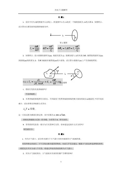
习 题11. 设在半径为R c 的圆盘中心法线上,距盘圆中心为l 0处有一个辐射强度为I e 的点源S ,如图所示。
试计算该点源发射到盘圆的辐射功率。
ΩΦd d e e I =, 202πd l R c =Ω 202e πd d l R I I c e e ==ΩΦ2. 如图所示,设小面源的面积为∆A s ,辐射亮度为L e ,面源法线与l 0的夹角为θs ;被照面的面积为∆A c ,到面源∆A s 的距离为l 0。
若θc 为辐射在被照面∆A c 的入射角,试计算小面源在∆A c 上产生的辐射照度。
用定义r r ee A dI L θ∆cos =和A E e e d d Φ=求解。
4. 霓虹灯发的光是热辐射吗?不是热辐射。
6. 从黑体辐射曲线图可以看出,不同温度下的黑体辐射曲线的极大值处的波长λm 随温度T 的升高而减小。
试由普朗克热辐射公式导出常数=T m λ。
这一关系式称为维恩位移定律,其中常数为2.898⨯10-3m ∙K 。
普朗克热辐射公式求一阶导数,令其等于0,即可求的。
9. 常用的彩色胶卷一般分为日光型和灯光型。
你知道这是按什么区分的吗?按色温区分。
习 题21. 何为大气窗口,试分析光谱位于大气窗口内的光辐射的大气衰减因素。
对某些特定的波长,大气呈现出极为强烈的吸收。
光波几乎无法通过。
根据大气的这种选择吸收特性,一般把近红外区分成八个区段,将透过率较高的波段称为大气窗口。
2. 何为大气湍流效应,大气湍流对光束的传播产生哪些影响? l 0 SR c 第1题图L e∆A s ∆A c l 0 θs θc第2题图是一种无规则的漩涡流动,流体质点的运动轨迹十分复杂,既有横向运动,又有纵向运动,空间每一点的运动速度围绕某一平均值随机起伏。
这种湍流状态将使激光辐射在传播过程中随机地改变其光波参量,使光束质量受到严重影响,出现所谓光束截面内的强度闪烁、光束的弯曲和漂移(亦称方向抖动)、光束弥散畸变以及空间相干性退化等现象,统称为大气湍流效应。
光电子课后习题答案
光电⼦课后习题答案第⼀章1. 光电⼦器件按功能分为哪⼏类?每类⼤致包括哪些器件?光电⼦器件按功能分为光源器件、光传输器件、光控制器件、光探测器件、光存储器件、光显⽰器件。
光源器件分为相⼲光源和⾮相⼲光源。
相⼲光源主要包括激光器和⾮线性光学器件等。
⾮相⼲光源包括照明光源、显⽰光源和信息处理⽤光源等。
光传输器件分为光学元件(如棱镜、透镜、光栅、分束器等等)、光波导和光纤等。
光控制器件包括调制器、偏转器、光开关、光双稳器件、光路由器等。
光探测器件分为光电导型探测器、光伏型探测器、热伏型探测器等。
光存储器件分为光盘(包括CD、VCD、DVD、LD等)、光驱、光盘塔等。
光显⽰器件包括CRT、液晶显⽰器、等离⼦显⽰器、LED显⽰。
2.谈谈你对光电⼦技术的理解。
光电⼦技术主要研究物质中的电⼦相互作⽤及能量相互转换的相关技术,以光源激光化,传输波导(光纤)化,⼿段电⼦化,现代电⼦学中的理论模式和电⼦学处理⽅法光学化为特征,是⼀门新兴的综合性交叉学科。
⒌据你了解,继阴极射线管显⽰(CRT)之后,哪⼏类光电显⽰器件代表的技术有可能发展成为未来显⽰技术的主体?等离⼦体显⽰(PDP),液晶显⽰(LCD),场致发射显⽰(EL),LED显⽰。
第⼆章:光学基础知识与光场传播规律⒈填空题⑴光的基本属性是光具有波粒⼆象性,光粒⼦性的典型现象有光的吸收、发射以及光电效应等;光波动性的典型体现有光的⼲涉、衍射、偏振等。
⑵两束光相⼲的条件是频率相同、振动⽅向相同、相位差恒定;最典型的⼲涉装臵有杨⽒双缝⼲涉、迈克⽿孙⼲涉仪;两束光相长⼲涉的条件是(0,1,2,)m m δλ==±± ,δ为光程差。
⑶两列同频平⾯简谐波振幅分别为01E 、02E ,位相差为φ,则其⼲涉光强为22010201022cos E E E E φ++ ,两列波⼲涉相长的条件为2(0,1,2,)m m φπ==±±⑷波长λ的光经过孔径D 的⼩孔在焦距f 处的衍射爱⾥斑半径为1.22fDλ。
南京邮电大学研究生光电子学理论与技术试卷
得分得分南京邮电大学 2014/2015学年第二学期研究生课程《 光电子学理论与技术 》试题院(系) 班级 学号 姓名装订线内不要答题自觉遵守考试规则,诚信考试,绝不作弊题号一二三四五六七八九十总分得分一、填空题(每空2分,共40分)1.光的基本属性是光具有波粒二象性,光粒子性的典型现象有光的 吸收、发射以及光电效应。
2.EDFA发展的目标主要有两个宽带化和大功率化。
3.PDFA是掺镨光纤放大器的缩写,它的工作波长范围为1281-1381um。
4. 光在各向同性介质中传播时,复极化率的实部表示色散与频率的关系,虚部表示物质吸收与频率的关系。
5.激光器的基本结构包括激光工作物质、泵浦源和光学谐振腔。
激光产生的充分条件是阈值条件和增益饱和效应,必要条件包括粒子数反转分布和减少振荡模式数。
6.PCM过程包括抽样、量化、编码。
7.声光互作用的两种类型为拉曼-纳斯衍射、布拉格衍射。
8.调制的类型有内调制、外调制。
9.光子与电子相比主要的优点有光子速度快、可传感多重信息。
二、证明与简述题(每题5分)1、证明如果是频率为的寻常波和频率为2的非常波的相位匹配角,则有证明:由相位匹配条件得:,则对求导,可得:,由此可得:2、什么叫声光调制?分哪几种类型?其判据是什么?。
答:声波的应变场也能改变某些类型晶体地折射率,由于声波的周期性,会引起折射率的周期性变化,产生类似于光栅的光学结构,从而对入射的光波产生调制,这种调制称为声光调制。
按照超声波频率的高低和光波相对声场的入射角度及两者相互作用的长度,将声光衍射分为拉曼一奈斯衍射和布拉格衍射两类。
拉曼一奈斯衍射与布拉格衍射的判断依据用声光相互作用特征长度Lo来表示:。
拉曼一奈斯衍射,布拉格衍射过渡区。
得 分3、举出几个你所知道的光电子技术应用实例。
答:如:光纤通信,光盘存储,光电显示器、光纤传感器、光计算机等等。
4. 对光进行外调制有哪些典型方式。
答:光外调制是在激光谐振腔以外的光路上放置调制器,将待传输的信号加载到调制器上,于是,当激光通过这种调制器时,激光的强度、位相、频率等将发生变化,从而实现调制。
固体光电子导论课后习题(南邮)
1.2 A 1.6 eV photon is absorbed by a valence band electron in GaAs. If the bandgap of GaAs is 1.41 eV, calculate the energy of the electron and heavy hole produced by the photon absorption. Condition:***0001.6 1.410.0670.450.058e h r eV Eg eV m m m m m m ω===== Solution: By2222***11()22e h rEg m m m ωωω-=+=We can get*22***22**()0.1642()0.0252e r c ee h r v h h m E E Eg eV m m m E E Eg eV m m ωωωω⎧-==-=⎪⎪⎨⎪-==-=⎪⎩1.4 The absorption coefficient near the bandedges of GaAs and Si are 4110cm - and 3110cm - respectively. What is the minimum thickness of a sample in each case which can absorb 90% of the incident light? Condition:3141()10()10Si cm GaAs cm αα--==Solution: By0min 0()()(190%)xI x I eI x I α-⎧=⎪⎨=-⎪⎩ We can getmin min min 00min ()0.10.11ln 0.1x x I x I e I e x ααα--==⇒=⇒=-So3min 4min () 2.310() 2.310x Si cmx GaAs cm--⎧=⨯⎪⎨=⨯⎪⎩1.8 In a GaAs sample at 300K, equal concentrations of electrons and holes areinjected. If the carrier density is n=p=1017cm -3, Calculate the electron and hole Fermi levels using the Boltzmann and Joyce-Dixon approximations.Condition:173183300,, 4.710710c v When T K for GaAs N cm N cm --==⨯=⨯Solution:Boltzmann approximation:ln 0.0402ln 0.1105nc c F B p c F v B N E E k T eV n N E E k T eVp ⎧-==⎪⎪⎨⎪-==⎪⎩Joyce-Dixon approximation:(ln 0.0383(ln 0.1103ncF B c p F v B v n E E k T eV N n E E k T eV N ⎧-=-=⎪⎪⎨⎪-=-+=⎪⎩1.12 The radiative lifetime of GaAs sample is 1.0 ns. The sample has a defect at the midgap with a capture cross-section of 10-15cm 2 . At what defect concentration does the non-radiative lifetime become equal to the radiative lifetime at i) 77K and ii) 300K?(分电子、空穴计算) Condition:**152000.0680.47 1.010n p r nr m m m m nscm ττσ-=====Solution:(1)For electrons7*277*2730013(77) 2.2710/2213(300) 4.4810/22th n th B K n th B Kth v K cm s m v k T m v k T v K cm s ⎧⎧==⨯⎪=⎪⎪⎪⇒⎨⎨⎪⎪===⨯⎪⎪⎩⎩So16316311(77) 4.4110(77)(77)11(300) 2.2310(300)(300)nr t t th nr th nr tt th nr th N K cm N v K v K N K cm N v K v K τστστστσ--⎧⎧===⨯⎪⎪⎪⎪⇒⎨⎨⎪⎪===⨯⎪⎪⎩⎩(2)For holes6*277*2730013(77)8.6310/2213(300) 1.7010/22th p th B K p th B Kth v K cm s m v k T m v k T v K cm s ⎧⎧=⨯⎪=⎪⎪⎪⇒⎨⎨⎪⎪===⨯⎪⎪⎩⎩So17316311(77) 1.1610(77)(77)11(300) 5.8810(300)(300)nr t t th nr th nr tt th nr th N K cm N v K v K N K cm N v K v K τστστστσ--⎧⎧===⨯⎪⎪⎪⎪⇒⎨⎨⎪⎪===⨯⎪⎪⎩⎩1.13 Electrons are injected into a p-type silicon sample at 300K. The e-h radiative lifetime is 1μs. The sample also has midgap traps with a cross-section of 10-15cm 2 and a density of 1016cm -3. Calculate the diffusion length for the electrons if the diffusion coefficient is 30 cm 2/s. Condition:1521632*01101030/ 1.08r t n n s cm N cm D cm s m m τμσ--===== Solution:By*2713 1.1210/22n th B th m v k T v cm s =⇒=⨯We get18.93nr t th ns N v τσ==Then1118.85rnrns ττττ=+⇒=So45.1510n L m -==⨯2.1 The bandgap of 1x x Hg Cd - alloy is given by the expression()0.3 1.9()Eg x x eV =-+Calculate the composition of an alloy which gives a cutoff wavelength of a) 10m μ b) 5.0m μ. Solution: By1.24c hc m Eg Egλμ==We get1.24 1.2410(10)0.220.3 1.91.24 1.24 5.0( 5.0)0.290.3 1.9c c c c m x m Eg xm x m Eg xλμλμλμλμ===⇒==-+===⇒==-+2.2 Calculate the cutoff wavelength for a GaAs detector. If the cutoff wavelength is to be decreased to 0.7μm, how much AlAs must be added to a GaAs? Assume that the bandgap of 1x x Ga Al As - is given by() 1.43 1.25()Eg x x eV =+ Solution: By1.24c hc m Eg Egλμ==We get1.24 1.240.7(0.7)0.271.43 1.25c c m x m Eg xλμλμ===⇒==+2.4 An optical power density of 1W/cm 2 is incident on a GaAs Sample. The photon energy is 2.0eV and there is no reflection from the surface. Calculate the excess electron-hole carrier densities at the surface and 0.5μm from the surface. The e-h recombination time is 10-8s. Condition:2418(0)1/() 2.1110 2.0010op P W cm GaAs cm w eV R s ατ--==⨯===Solution: (1)At the surface2231()(0)(0) 6.5910op L GaAs P G cm s wα--==⨯So143(0)(0)(0) 6.5910L n x p x G cm δδτ-=====⨯(2)At 0.5m μ from the surface()2(0.5)(0)0.35/GaAs xop op P x m P eW cm αμ-=== 2231()(0.5)(0.5) 2.3110op L GaAs P x m G x m cm s wαμμ--====⨯So143(0.5)(0.5)(0.5) 2.3110L n x m p x m G x m cm δμδμμτ-======⨯2.5 Assume that all the photons in an optical beam produce an electron-hole pair in a Ge detector. If all the carriers are collected calculate the responsivity for photon energies of a)0.7eV b)1.0eV c)2.0eV. Condition:1Q η= Solution: ByQ phhvR eη=We get111(0.7) 1.43( 1.0)1( 2.0)0.5Q ph Q ph Q ph e R hv eV V hv e R hv eV V hv e R hv eV V hvηηη---=========2.6 Consider a long Si p-n junction with a reverse bias of 1V at 300K. The diode has the following parameters:2173173227731213101012/8/10101010/ 1.7a d n p n p op A cm N cm N cm D cm sD cm ssscmP W cmw eVττα-----==⨯========Calculate the photocurrent in the diode. Solution: By22313.6810opL P G cm s wα--==⨯10.95n L m μ==8.94p L m μ==2ln()0.846a d B bi iN N k TV V e n == 1/202{()()}0.18r a d bi a dN N W V V m e N N εεμ+=+= So()11.8L L n p I eAG W L L A =++=2.7 Consider a long Si p-n junction solar cell with an area of 4cm 2 at 300K. The solar cell has the following parameters:17318322773101015/7.5/1010 1.0 1.25a d n p n p L N cm N cm D cm s D cm sss I Am ττ----=⨯=======Calculate the open circuit voltage of the diode. If the fill factor is 0.75,calculate the maximum power output. Solution:By1202012.258.667.1410n p n p p n p n i n p n a p d L m L mI A eD n eD p D D I A Aen L L L N L N μμ-⎧⎪==⎪⎪=⇒=⨯⎨⎪⎛⎫⎛⎫⎪=+=+ ⎪ ⎪⎪ ⎪ ⎪⎝⎭⎝⎭⎩ We getln(1)0.83L oc I mkTV V e I =+= And0.6225m f oc L P F V I W ==2.8 Consider the solar cell of problem 2.7.A solar system is to be developed from such cells to deliver a power of 15W at a voltage level of 5V. Calculate the total number of solar cells needed. Condition:10.830.75sc oc f I A V V F ===Solution:For each solar cell:0.870.72m sc m oc I A V V⎧==⎪⎨==⎪⎩ We can get5()[]1715()[]145mmN series V N para I =+==+=So the total number of cells()()28Tot N N series N para =⋅=2.10 Consider a silicon photoconductor at 300Kwith the following parameters:153226742101200/400/1051010100d n p n p N cm cm V scm V s ssA cmL mμμττμ----==⋅=⋅==⨯==A bias of 5V is applied to the detector. Calculate the dark current. If light falls on the detector to produce a generation rate of 1021cm -3s -1,calculate the excess concentration, the photoconductivity, and device gain. Solution:(1) The dark current0000015302530()()109.6/ 2.2510B dn p n p d d i d V I FA e n p AF e n p A Ln N cmI mA p n N cm σμμμμ--⎧==+=+⎪⎪⎪==⇒=⎨⎪==⨯⎪⎪⎩(2) The excess carrier denisty143510L p p n G cm δδτ-===⨯(3) The photoconductivity()10.128n p e n p s cm σμδμδ-∆=+=⋅(4) The device gain8(1)401.6710pp L ph Lptr n ph tr n I G I t G L t s F τμμμ-⎧==+⎪⎪⇒=⎨⎪==⨯⎪⎩2.13 Consider a GaAs p-i-n detector with an intrinsic layer width of 1.0 μm. Optical power density (photon energy 1.6eV) of 0.1W/cm 2 impinges upon the detector. The absorption coefficient for the active region is 104cm -1. Calculate the prompt photocurrent of device. The device area is 10-4cm 2. Condition:241421.0 1.60.1/1010op W m w eVP W cm cm A cm μα---=====Solution:17216(0) 3.9110 3.9510(0)[1exp()]op ph L L ph P J cm s I A I eAJ W ωα---⎧==⨯⎪⇒=⨯⎨⎪=--⎩2.14 Consider a silicon p-i-n detector in which the i layer is 10 μm thick. Calculate the maximum quantum efficiency of this detector if only light absorbed in the undoped region contributes to the photocurrent. The absorption coefficient for the active region is 103cm -1. Also calculate the minimum thickness of the i-region needed to ensure a quantum efficiency of 0.8. There are no reflection losses. Condition:3110100.80Q W mcm R μαη-====Solution: (1) By()2max 1exp 10.86412[,]W e W ηαηαα=--⎧⎪⇒=-=⎨∈⎪⎩(2) By()min min 311exp 0.816.110W W m cmηαμα-⎧=--=⎪⇒=⎨=⎪⎩2.16 An avalanche photodetector has an avalanche region of 0. 5μm and the electric field is such that αimp =βimp =104cm -1. Calculate the multiplication factor of the device. Solution:121e imp M Wα==-3.8 Consider a GaAs p-n + junction LED with the following parameters at 300K:2217316325/12/510101010n p d a n p D cm sD cm sN cm N cm ns nsττ--===⨯===Calculate the injection efficiency of the LED assuming no trap related recombination. Solution: By(1)(1)B B eVn p k Tn n eVp n k T p p eD n J e L eD p J e L ⎧=-⎪⎪⎨⎪=-⎪⎩And24326341053.46810i p n a i p n d n n cm L mN n L m p cm N μμ----⎧==⨯⎪⎧==⎪⎪⎨⎨==⎪⎪⎩==⨯⎪⎩We can get0.986n pn ninj n p p nn p n peD n J L eD n eD p J J L L γ===++3.9 The diode in Problem 3.8 is to be used to generate an optical power of 1mW. The diode area is 1 mm 2 and the radiative efficiency is 20%. Calculate the forward bias voltage required. Condition:21120%out Qr P mWA mm η===Solution:By53.54410out ph ph n nQrph QrP I wI e I A I I e ηη-=⋅⎧⋅⎪⇒==⨯⎨=⋅⎪⎩Andexp 1n p n n n B AeD n eVI J A L k T⎡⎤⎛⎫=⋅=-⎢⎥ ⎪⎝⎭⎣⎦Soln 1 1.02n p B n n AeD n k T V V e I L ⎡⎤=+≈⎢⎥⎣⎦3.12 The light from a GaAs LED is coupled into an optical fiber which has refractive indices of 1.51 and 1.47 for the core and the cladding layers. Calculate the maximum angle of acceptance for the fiber. The LED has a Lambertian(cosine) output. Calculate the coupling efficiency for the diode. Condition:121.51 1.47r r n n == Solution:1221/2122sin ()20.2sin 0.12A r r fiber A n n θηθ-=-===3.15 Consider an AlGaAs/GaAs heterojunction LED. The injection densities for electrons and holes are equal and are both 1017 cm -3 In the active GaAs region. Calculate the shift in the peak position of the emission peak energy if E g (GaAs) is 1.43eV. Calculate the shift in the peak position if the injection density is increased to 1018cm -3 . The temperature is 300K. Condition:17310 1.43n p cm Eg eV -===Solution:(1) For injection density of 17310n p cm -==0.026E kT eV ∆==111.4432p g E E E eV ≈+∆=(2) For injection density of 18310n p cm -==0.055cnE kT eV N ∆== 211.4582p g E E E eV ≈+∆=So120.015p p E E E eV ∆≈-=3.18 A heterojunction LED based on GaAs is biased at 100Acm 2 current density at 300K. The active layer of LED is 0.5μm. Calculate the cutoff frequency of the diode. Condition:21000.5J A cm d m μ=⋅=Solution: ByrdJ nev ne τ==25311.2510rnJcm s edτ--⇒==⨯⋅ From the Fig 1639910810rn cm s τ--⨯⨯So119.92c rf MHz πτ=≈3.21 A GaAs LED is to be designed with an output power of 5.0W. The maximum device area that can be allowed 100 μm 2.Estimate the thickness of the active region needed. The efficiency of the Device is 20%. The maximum injection density is 1018cm -3. Condition:21835.010020%10out Tot P W A m n cm μη-====Solution:ph rI ndAP I e ωωηηωτ===2.2rd m nAμηω==3.22 Consider a GaAs p-n + junction LED with the following parameters at 300K:110.2 3.0 2.0inj opt r nr P mWns ns γηττ=====Calculate:a) the total quantum efficiency of LED ηtotal ;b) the number of photon generated per second I ph ; c) the injected current I inj . Solution:(1) 10.40.0811rQr Tot inj Qr opt rnrτηηηηηττ==⇒==+(2) 1611610.43710 2.18510opt ph ph opt P P I s I s w w ηη--==⨯⇒==⨯⋅ (3) 8.74phinj ToteI I mA η==4.1 Consider a GaAs laser with a cavity length of 75μm. Calculate the number ofallowed longitudinal modes in an energy width 12g B E k T ± where Eg=4.43eV andT=300K. Solution:115.5102r cHz n Lν∆==⨯ 112E N h ν∆⎡⎤=+=⎢⎥∆⎣⎦4.3 Consider a Fabry-Perot cavity of length 100μm. The mirror reflectivity is 0.33 and the absorption loss in the cavity is 120cm -.Calculate the photon lifetime ph τ.The refractive index in the cavity is 3.6. Condition:11000.3320 3.6loss r L mR cm n μα-====Solution:-1ln 130.866cm Tot loss R Lαα=-=139.1710rph Tot n s cτα-==⨯4.8 Two GaAs/AlGaAs double heterostructure laser are fabricated with active region thickness of 2.0μm and 0.5μm. The optical confinement factors are 1.0 and 0.8, respectively. The carrier injection density needed to cause lasing is 1831.010cm -⨯ in the first laser and 1831.110cm -⨯ in the second laser.The radiative recombination times are 1.5ns.Calculate the threshold current densities for the two lasers. Solution:42113222 2.1310/5.8710/lasth th rlasth th rd J n eA cm d J n eA cm ττ==⨯==⨯5.1 A GaAs/AlGaAs laser has a threshold current density of 200A/cm -2. In a large signal switching, the laser is switched from zero current to 4 times the threshold current . Calculate the time delay before photon emission if the carrier lifetime is 2ns. Solution:ln()0.575d thJt ns J J τ==-5.2 A 1.55μm quantum well laser has a threshold carrier density of 2∙1012 cm -2.The radiative lifetime is 2.5ns and Auger coefficient is 10-28cm 6s -1.Calculate the time delay for a large signal switching in which the current density isswitched from 0.5J th to 3.0J th . Assume that the Auger rate can be evaluated using the carrier density n th . The active layer thickness is 10nm. Condition:12228612210 2.51010D r las n cm nsF cm s d nm τ---=⨯===Solution:1832210Dth lasn n cm d -==⨯ 21() 2.5nr th Fn ns τ-⇒==111() 1.25r nr ns τττ---⇒=+=So()ln()0.28d thJ J i t ns J J τ-==- 6.1 Condition:GaAs/AlGaAs TW amplifier1582210 1.43510410 1.0200 1.0m in dgeVA cm cm nsdng cm P mWωτ---==⨯=⨯===Calculation: saturation power P s , the gain Solution:2.86ms A P mW dg dnωτ==10148.21sg g cm P P -==+。
光电子学(南邮)全部作业答案
40
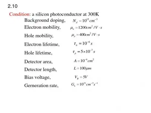
2.13
Condition: a GaAs p-i-n detector with
Intrinsic layer width, W 1.0m Optical power density, Pop 0.1W / cm2
Photon energy,
1.6eV
Absorption coefficient, 104cm1
n-side doping,
N d 5 1017 cm 3
p-side doping,
N a 1016 cm3
Electron minority carrier lifetime, n 10ns
Hole minority carrier lifetime, p 10ns
Calculation: the forward bias voltage required.
Solution: The photons generated per second are
I ph
Power
103 (1.41)(1.6 1019 )
4.431015 s 1
Which are also expressed by
Id (1.61019C)[(1200cm2 /V s)(1015cm3) (400cm2 /V s)(2.25105cm3)](104cm2)(5 /100104V / cm) 0.0096A 9.6mA
b)The excess carrier density is
Electron lifetime, Hole lifetime,
n 106 s p 5107 s
Detector area, Detector length,
电工电子学 第二章习题参考答案
( 2 ) S 断 开 时 , A1 的 读 数 为 14.25 A , A2 的 读 数 为 4.75 A ;
iU = 2 ×14.25sin(314t − 36.87D ) A
2.4.7 C)
2.5.1 uo = 100 + 3.74 2 sin(2ωt −175.4D ) + 0.374 2 sin(4ωt −177.7D ) V
2.3.7 ω =1000 rad/s 时 , Z =( 500-j1500) Ω =1581 ∠ − 71.6D Ω 、
i = 10.1 2 sin(1000t + 71.6D ) mA ;
ω =2000 rad/s 时,Z = 500 Ω 、 i = 32 2 sin 2000t mA ;
ω =3000rad/s 时 , Z =( 500+j833.3)= 971.8∠59D Ω 、
2.4.5
•
IU
= 33.15∠15.14D
A
•
、I V
= 13.2∠ − 79.11D
A
•
、I W
= 13.2∠ −199.11D
A,
•
中线电流 I N = 22 A
2.4.6 (1)电流表 A1 的读数为 16.45 A ,电流表 A2 的读数为 9.5 A ;相量
图(略); iU = 2 ×16.45sin(314t − 66.87D ) A
•
I
= 10∠
− 15D
A ,i = 10
2 sin(314t − 15D ) A
2.3.4
(1)iR
=
u R
= 2.2
2 sin 314t
A
iC = 0.69 2 sin(314t + 90D ) A
光电子习题及答案
光电子习题及答案光电子习题及答案光电子学是研究光与电子相互作用的学科,它广泛应用于光电器件、光通信、光储存等领域。
在学习光电子学的过程中,习题是检验自己理解和掌握程度的重要方式。
下面,我们来讨论一些光电子学的习题及其答案。
1. 什么是光电效应?它与光子和电子之间的相互作用有什么关系?光电效应是指当光照射到金属或半导体表面时,会引起电子的发射现象。
光电效应的基本过程是光子与金属或半导体中的电子相互作用,使得电子获得足够的能量从而逃逸出材料表面。
光电效应的关键在于光子的能量必须大于或等于材料中电子的逸出功,才能引起电子的发射。
2. 什么是光电子倍增管?它的工作原理是什么?光电子倍增管是一种利用光电效应和二次发射效应来放大光信号的器件。
它由光阴极、倍增极、收集极和阳极组成。
当光照射到光阴极上时,光子与光阴极表面的电子发生光电效应,产生光电子。
这些光电子经过倍增极的二次发射作用,使得光电子的数量增加。
最后,这些光电子被收集极吸收,产生电流信号,经过放大后输出到阳极。
3. 什么是光电二极管?它与普通二极管有什么不同?光电二极管是一种利用光电效应来转换光信号为电信号的器件。
它由光阴极、势阻极和阳极组成。
当光照射到光阴极上时,光子与光阴极表面的电子发生光电效应,产生光电子。
这些光电子经过势阻极的势垒层,产生电流信号,经过放大后输出到阳极。
与普通二极管相比,光电二极管对光信号更加敏感,能够将微弱的光信号转换为电信号。
4. 什么是光通信?它的优势和应用领域有哪些?光通信是利用光信号传输信息的通信方式。
它通过光纤或自由空间传输光信号,具有大带宽、低损耗、抗干扰等优势。
光通信广泛应用于电话、互联网、电视等领域。
在长距离通信中,光通信可以实现高速、大容量的数据传输,满足现代社会对通信带宽的需求。
此外,光通信还被用于军事通信、卫星通信等领域。
5. 什么是光储存?它的原理和应用有哪些?光储存是利用光信号存储和读取信息的技术。
南京邮电大学光纤习题解题指导(部分)
27
Chap.3 No.11 光发送机中输入接口的作用是什么?
对驱动电路有什么要求?
输入接口除了正常应该考虑信号幅度大小和阻抗外, 特别应注意信号脉冲码型,即将原始信息变换为适宜于在 光纤中传输的码型。 对驱动电路要求: 输出的光脉冲峰值必须保持恒定。 光脉冲的通断比(即消光比)应≥10,以免接收灵敏度 受到损害。 电流脉冲加上后,激光发射的时间必须远短于每位码元 的时间段。 如加上的电流脉冲有较高的码速,则输出的光脉冲有可 能引起弛张振荡,这就必须予以阻尼,防止它对系统性能 发生不良影响
详见光发送电路部分,重点理解注入电流信号与 阈值电子密度和光子密度之间的关系,以及由此产生 的驰张振荡和暂态过击现象。 解决方法是实现在光源电路中加入偏置电流,其 选取原则是略小于阈值电流。
20
Chap.3 No.4 已知半导体材料GaAs的Eg=1.43eV, InGaAsP的Eg=0.96eV,分别求由这两种材料组成的半 导体激光器的发射波长。
习题解题指导
南京邮电大学 通信与信息工程学院
Chap.1 No.1 光纤通信有哪些优点?
参见1.2.1。
2
Chap.1 No.2 比较五代光纤通信系统的主要特点与差别。
参见1.1,注意各代系统在传输容量和关键技术上 的区别。
3
Chap.1 No.3
为什么使用石英光纤的光纤通信系统中,工作波长只能选择 850nm、1310nm、1550nm三种。
参见2.5.2,最大理论数值孔径为
NAt ,max n 2 (0) n 2 ( a )
入射点处局部数值孔径为
NA( r ) n ( r ) n ( a )
2 2
13
Chap.2 No.10 某阶跃折射率光纤的参数为……试问该入 射光线在光纤中是成为传导模还是辐射模?为什么?
南京邮电大学《电工电子实验(二)》2022-2023学年的第二学期期末试卷
南京邮电大学《电工电子实验(二)》2022-2023学年的第二学期期末试卷《电工电子实验(二)》考试内容:《电工电子实验(一)》;考试时间:120分钟;满分:100分;姓名:——;班级:——;学号:——一、选择题(每题2分,共20分)1. 在进行模拟电路实验时,用于信号放大的主要元件是:A. 电阻B. 电容C. 运算放大器D. 二极管(但在此作为放大器使用时,通常与电阻等元件组合形成放大电路)2. 下列哪个实验主要用于验证数字电路中的逻辑运算规则?A. 戴维南定理实验B. 叠加定理实验C. 数字逻辑门电路实验D. 三相异步电动机启动实验3. 在示波器上调整波形垂直方向的幅度,应使用哪个旋钮?A. 扫描速度旋钮B. 垂直位移旋钮C. 垂直幅度旋钮D. 触发方式选择4. 逻辑表达式 F = A + BC 对应的门电路组合是:A. 与门和或门B. 或门和非门C. 与门、或门和非门的组合D. 仅需要或门5. 三相电源中,线电压与相电压的关系是(在星形连接且平衡负载情况下):A. 线电压等于相电压B. 线电压等于相电压的√3倍C. 线电压等于相电压的一半D. 线电压与相电压无关6. 使用数字万用表测量电阻时,若选择量程过大,可能导致的后果是:A. 测量值偏大且不准确B. 测量值偏小且不准确C. 万用表损坏D. 无影响,只是读数可能较慢7. 下列哪个不是常用的模拟信号处理方法?A. 滤波B. 放大C. 采样D. 调制8. 在进行半导体二极管正向导通压降测量时,应给二极管施加:A. 正向高电压B. 正向低电压C. 反向电压D. 任意电压9. 555定时器构成的多谐振荡器电路中,用于控制振荡频率的主要元件是:A. 电阻B. 电容C. 电阻和电容的组合D. 运算放大器10. 在数字电路实验中,若要实现一个四输入的逻辑与(AND)功能,最少需要的基本逻辑门是:A. 1个B. 2个C. 3个D. 4个。
二、填空题(每空2分,共20分)1. 在模拟电路实验中,常用_______来表示电路中的非线性元件,如二极管和晶体管。
- 1、下载文档前请自行甄别文档内容的完整性,平台不提供额外的编辑、内容补充、找答案等附加服务。
- 2、"仅部分预览"的文档,不可在线预览部分如存在完整性等问题,可反馈申请退款(可完整预览的文档不适用该条件!)。
- 3、如文档侵犯您的权益,请联系客服反馈,我们会尽快为您处理(人工客服工作时间:9:00-18:30)。
2.5-4、条形激光器按在侧向的波导机构可以分为那两类? 有什么区 别?
答:条形激光器按它们在侧向的波导机构分为两类,即增益波导与折
射率波导。
增益波导是半导体芯片纵向中心区域内形成一注入电流的通道,使 有源层中心部分的增益(或复介电常数的虚部)高于其两侧; 侧向折射率波导是由有源层与其两侧材料的折射率差来实现的。
可用深锌扩散的方法使所需的电流通道区相对于两侧形成低阻区,
更有效的方法是采用反向pn结阻止电流的扩展。 为防止载流子的侧向扩散,可采取以下措施: (1)限制注入电流的侧向扩展; (2)在有源区两侧侧用pn同质结势垒限制载流; (3)在侧向用异质结对载流子的侧向扩散进行限制。
作业: 补充1-3题
(2.4节)1、描述单异质结半导体激光器的结构。解释说明其 相对于同质结的优越性。并说明其缺点。
e 20 30 h
同质结LED为提高注入效率,应采用P区作为出光区,使电子注入电流尽 量大,空穴注入电流尽量小;
在异质结LED中,N区和P区分别向有源区注入电子和空穴,且有源区两
边异质结的势垒可限制注入该区的两种载流子;电子和空穴复合产生的光子, 无论从P区还是N区出射,都不会被吸收,因此并不局限在以P区作为出光区。
【解】 (1)总量子效率;
Qr
1 1 r nr 1 0.7143 125
Tot inj Qr opt 0.8 0.25 0.714 0.143
(2)单位时间内产生的光子数
I ph
P opt
1.5 103W 16 1 2.62 10 s 19 h 0.25 1.43 1.6 10 J
【习题2.5】GaAs材料制作的P-N+同质结LED,器件参数如下。请计算:
(1)总量子效率;
(2)单位时间内产生的光子数;
(3)注入电流。
输出光功率 注入效率 出光效率 辐射复合寿命 非辐射复合寿命
P 1.5mW
inj 0.8 opt 0.25 r 2.0 ns nr 5.0 ns
Ln Dn n (25)(10 )
8 12
2
扩:
D p p (12)(10 )
8
12
3.46 m
inj
eD n n po 25 4 104 4 Ln 5 10 eD n n po eD p p no 25 4 104 12 8 106 4 5 10 3.46 104 Ln Lp
振荡或形成稳定的驻波。
4πn r1r2 exp j L 1 o
3. 光子在腔内形成稳定振荡的阈值振幅条件和相位条件。
r1r2 exp( g i ) L 1
4πn exp j L 1 o
应,限制了有源区中所激发的光子从横向逸出该异质结而损失掉;单
异质结已使激光器的阈值电流密度比同质结激光器低一个数量级。 pn 同质结对注入有源层的空穴向 n 区扩散没有限制,同时对光子
也只有很弱的光波导效应。因此,为了达到粒子数反转所需的载流子
浓度,仍需在n区重掺杂(3~4×10¹⁸/cm3)
(2.4节)2、描述双异质结半导体激光器的结构。并简要说明其 优点。 答:
更高。
【习题2.1】
P-N+型同质结构成的LED,参数如下。计算其注入效率。
电子扩散系数 空穴扩散系数 N区 掺 杂 浓 度 P区 掺 杂 浓 度 电子少数载流子寿命 空穴少数载流子寿命 Dn 25cm2 / s D p 12cm2 / s N d 5 1017 cm3 N a 1016 cm3
【习题2.3】 P-N+型同质结构成的LED,参数与习题2.1相同,其
产生光功率为1mW,器件横截面积为1 mm2,辐射效率为20%。求正 向偏置电压。 (工作温度300 K)
【解】 I ph
I ph
In
V
Power 103 15 1 4.37 10 s 19 (1.43)(1.6 10 )
答: (1)同质结LD有源区的厚度主要由p区电子的扩散长度所决
定;而它是随温度的增加而增加的,室温时的Ln可达5微米。
在如此厚的有源区内实现粒子数反转,需要大的注入载流子
浓度; 在一个Ln范围内产生的受激辐射光子,无限制地向两边扩展;
所以,同质结LD阈值电流密度高,而且随温度发生剧烈变化。
同质结室温下的阈值电流密度高达 104A/cm2量级,只能在液 氮温度下才能连续工作; (2)结附近存在一个很小的折射率台阶,引起一个很弱的光 波导效应,但由于电子有比空穴高的迁移率因而有大的扩散 长度,所以同质结半导体激光器的有源区偏向p区一侧。
(3)注入电流
e I ph 1.6 1019 2.62 1016 I 7.35mA Qr inj 0.7143 0.8
或 tot
P h I e
eP 1.6 1019 1.5 103 I 7.35mA 19 tot h 0.143 (1.43 1.6 10 )
双异质结半导体激光器的结构:有源层p-GaAs被夹在宽带隙材料 P-GaAlAs和N-GaAlAs之间。 优点:由于利用双异质结对载流子和光子的限制作用加强,阈值电流密 度比单异质结结构下降了近一个数量级; 双异质结结构上的对称性,带来了折射率和光强分布的对称性。
(2.4节) 3、目前对异质结半导体LD的研究主要集中在哪些方面?
2.2节思考题 1 :
为什么在同质结LED中,应该使电子注入电流尽量大,空穴注入电流
尽量小,或者说用P区作为出光区,而在异质结LED中,并不需要这样做?
同质结LED的注入效率:
inj
Jn Jn J n J p J GR J n J p
Jn ND J p NA
e h h e
答:单异质结半导体激光器由一个同质结和一个异质结构成,有源
层(p-GaAs)被夹在(n-GaAs)和宽带隙材料(P-GaAlAs)之间。
从 n-GaAs 注入 p-GaAs 的电子就会受到 p-GaAs/P-GaAlAs 异质结 势垒的限制,在同样的注入速率下,这将使有源层积累的非平衡少数 载流子浓度增加;同时异质结两边材料的折射率差所形成的光波导效
激光器的基本组成部分:
增益介质
谐振腔 泵浦源
优点:
结构很紧凑,避免了外加谐振腔可能产生的机械不稳定性; 半导体激光器的驱动电源也较简单,需要的电流、电压均很小, 因此工作较方便和安全。
2. 什么是半导体激光器的阈值条件?
阈值条件: 光子在谐振腔内往返一次,不产生损耗而能维持稳定的
【习题2.6】 GaAs材料的LED,输出功率为5 mW,横截面积100um2,
器件出光效率为0.2,载流子的辐射复合寿命为5ns。器件的非辐 射复合忽略不计,注入效率为1。计算有源层厚度是多少。
(题目中取n=1018cm-3)
I ndA e r
【解】
P I ph
In Qr e
eI ph
Qr
(1.6 1019 C )(4.37 1015 s 1 ) 3.49mA 0.2
I L kT ln(1 n n ) e AeDn n p
(3.54 103 A)(5.0 104 cm) (0.026) ln[1 ] 1.02V 2 2 19 2 4 3 (10 cm )(1.6 10 C )(25cm / s)(4 10 cm )
(2.5节)3.在条形半导体激光器中测向电流扩展和侧向载 流子扩散在物理概念上有何不同?如何减少这两种影响?
答:电流与载流子的侧向扩展都是载流子运动的结果,但前 者是 pn 结间多数载流子在电场作用下侧向的漂移运动,而后者 是注入的非平衡少数载流子由中心向两侧所形成的浓度梯度使其
产生侧向扩散。
为减少侧向电流扩展,必须形成良好的电流通道。可用质 子轰击或氧注入的方法在所需的电流通道区两侧形成高阻区;也
思考题 2 :
与普通的面发射LED相比较,为什么边辐射LED与光 纤之间的耦合效率更高?
对于普通面发射LED,由于在水平和垂直方向都没有限制, 因此其水平和垂直方向的散射角都为120°;
而对于边发射LED,虽然平行于结平面方向没有限制,水
平散射角虽仍是 120°;但在垂直于结平面方向对光有限制, 其垂直散射角是 30°,因此边辐射LED与光纤之间的耦合效率
n 10 ns p 10 ns
inj
eD n n po Ln eD n n po eD p p no Ln Lp
【解】 少子浓度为
ni (2 106 )2 4 3 np 4 10 cm Na 1016 2 ni (2 106 )2 6 3 pn 8 10 cm 17 5 10 Nd
答:(1)提高激光器工作寿命,研究激光器性能退化和失效
的机理,提高激光器长期工作的稳定性与可靠性,发展各种条形 结构的激光器,降低阈值电流。
(2)扩展半导体激光器的工作波段。
( 3)压缩半导体激光器输出光谱宽度(线宽)和适用在高速 调制下的单纵模工作(即动态单纵模)。 ( 4)提高半导体激光器的输出功率和输出光束的相干性,使 光子从信息领域扩展到以光子为能量载体的材料加工领域。
P r (5 103W )(5 109 s) d 5.5 m 19 18 3 8 2 nA (0.2)(1.43)(1.6 10 J )(10 cm )(100 10 cm )
2.3节思考题:
1. 激光器的基本结构由哪几部分组成?
半导体激光器有什么突出特点?
o2 do o dn 2nL 1 n d o