
字符叠加芯片MB90092手册中文版
屏幕显示控制的专用标准产品CMOS屏幕显示控制芯片——MB900921.描述MB90092是用于显示控制视频中的文字和图像的视频显示控制芯片,内部集成了显示内存(VRAM)、外挂字库接口和视频信号发生器,其外部只需连接少量的电子元件就可以显示汉字和图形。
MB90092提供两种屏幕叠加方法,分别称为“主屏”和“副屏”,二者可单独或相互重叠出现在监视器上。
主屏由12行24个字符组成,允许设置每个字符的数据。
副屏由12行24个字符组成或最多达到16行24个字符。
数据不仅可以在前期配置的每行中被设置,也可以集中地在后期配置的整个屏幕中被设置。
MB90092所支持的字符为24×32点阵的普通字符和8×32点阵的图形字符,这些字符单元可以任意八种不同的颜色显示。
如果主屏中只有图形字符,则有192×384个像素点,在同样的情况下,副屏有192×384个像素点或256×512个像素点。
(实际显示屏由水平方向的像素点的时钟频率和电视系统垂直方向的一定光栅数决定。
)MB90092把RAM作为字库内存,能够显示自由图形。
MB90092总共能够使用16384种类型的字符,包括普通字符和图形字符。
它能够控制外部16M bits的字库内存。
对于视频信号的输出,MB90092具有合成视频信号,Y/C分离视频信号,RGB数字信号输出引脚。
MB90092还具有视频信号输入引脚,允许重叠显示任意一种复合视频信号和Y/C分离视频信号。
2.封装80个引脚的PQFP封装3.特性3.1主屏显示•屏幕显示能力:24字符×12行(达到288字符)•字符点配置:24×32点(每个字符)•字符类型:16384种字符(当使用16M比特的外部时钟)•字符大小:标准,双宽度,双高度,双宽度×双高度,四倍宽度×双高度(每行可设置)•显示位置控制:水平显示位置:1/3字符单元设置垂直显示位置:光栅单元设置行空间控制:光栅单元设置(0~15光栅)•显示优先级控制:副屏显示控制优先级的能力3.2副屏显示屏幕显示位置:可设置的水平和垂直为2个点单元•普通屏幕模式:屏幕显示能力:32字符×12行(达到384字符)56×384点(仅限图形字符)(实际显示屏幕由电视系统和点时钟频率决定)。
普通字符/图形字符显示每行可供选择。
(每行的头显示字符对于是特定的。
)•全屏模式:屏幕显示能力:32字符×16行(达到512字符)256×512点(仅限图形字符)(实际显示屏幕由电视系统和点时钟频率决定)。
•虚拟屏幕显示能力:模式A:32字符×16行,256×512点模式B:512字符×32行,4096×1024点3.3屏幕背景显示屏幕背景颜色:8种颜色•模拟输入复合视频信号输入Y/C分离视频信号输入•模拟输出复合视频信号输出Y/C分离视频信号输出3.4数字输出G(绿色),R(红色)和B(蓝色)输出VOC(字符)输出,VOB(字符+背景)输出字符,字符背景,行背景和屏幕背景都可以8种颜色显示3.5内部同步控制(视频信号产生器)内部信号产生支持NTSC和PAL制系统隔行/逐行扫描显示选择3.6外部同步控制分离同步信号输入/复合同步信号输入选择3.7外部接口8-bit 串行输入(3个信号输入引脚)芯片选择:/CS串行时钟:SCLK串行数据:SIN3.8封装QFP-803.9其他内部开机复位电路4.引脚分布5.组成框图6.绝对最大额定值7.电气特性7.1直流特性7.1.1 VOUT 信号输出7.1.2 YOUT 信号输出7.1.3 COUT信号输出7.2交流特性7.2.1串行输入时序7.2.2垂直和水平同步信号输入时序7.2.3复位信号输入时序7.2.4地址数据保持时序7.2.5 TSC输入时,地址和READ信号延时时序图7.3时钟定时规范7.4开机复位规范7.5电源ON/OFF时序7.6上电复位取消时序8.典型电路这是一个标准的电路实例,用来对输入视频信号或从外面输入到内部所生成的视频信号叠加字符。
其构成随着系统和部件不同而不同。
9.显示控制命令7654321076543210010000VSL RA 8RA 70RA 6RA 5RA 4CA3CA 2CA 1CA 0VRAM 地址控制1—110001M A M B A T 0CG CR CB M C BG(GR)BG(BS)BB(M D)主屏字符控制12—110010M 9M 8M 70M 6M 5M 4M 3M 2M 1M 0主屏字符控制21—210001SM A SM B 00SCG SCR SCB SM C SGR SDC SM D 副屏行控制12—210010SM 9SM 8SM 70SM 6SM 5SM 4SM 3SM 2SM 1SM 0副屏行控制21—310001OF1OF000000PC PG PR PB 主屏行控制12—310010G2G1G00SOC VD DG KC KG KR KB 主屏行控制2310011FIL 0000000000VRAM 写控制410100IE IN EB 0EO CM ZM NP P2P0DC 屏幕控制1510101KID A PC GYZ 0BH2BH1BH0W 3W 2W 1W 0屏幕控制2610110G2G1G00SOC VD DG N3N2N1N0主屏行控制3710111EC LP FO 00Y5Y4Y3Y2Y1Y0主屏垂直位置控制811000SC 0FC 00X5X4X3X2X1X0主屏水平位置控制91100100GRM 00000000汉字字体显示控制101101000RB 0BK CC BC UC UG UR UB 颜色控制1111011SG2SG1SG000SCC SBC SGC SBG SBR SBB 副屏控制1211100SGA 0SY70SY6SY5SY4SY3SY2SY1SY0副屏垂直位置控制13111010SX8SX70SX6SX5SX4SX3SX2SX1SX0副屏水平位置控制1411110———0———————(保留)1511111——————————(保留)第一个字节第二个字节命令代码/数据数据命令号功能9.1命令0(VRAM 地址设置)[命令格式]第一字节第二字节[描述]VSL :VRAM写控制RA8 ~ RA5:VRAM 行地址设置(00 ~ BH)CA4 ~ CA0:VRAM 列地址设置(00 ~ 17H )9.1.1在正常模式下 (命令9: GRM = 0)MC ~ M0:设置一个字符代码0000H~1FFFH之间可以设置指定的字符代码。
多达8192个不同的字符都可以使用。
AT:指定字符显示属性。
AT = 0:指定正常显示。
AT = 1:指定属性显示。
固体填充背景(当命令10:RB = 1)闪烁(当命令10:BK = 1)阴影背景(当命令1:BS = 1)注:如果阴影背景显示和固体填充背景显示或闪烁显示都被指定,那么阴影背景显示设置的优先级高于其他设置。
CG,CG,CR:字符颜色BG,BR,BB:字符背景颜色9.1.2在扩展图形模式(命令9:GRM= 1)MD~M0:设置字符代码。
0000H~3FFFH之间可以设置指定的字符代码。
多达16384个不同的字符都可以使用。
AT:指定字符属性显示。
AT = 0:指定正常显示。
AT =1:属性变换显示开。
固体填充背景(当命令10:RB = 1)闪烁(当命令10:BK = 1)阴影背景(当命令1:BS = 1)注:如果阴影背景显示和固体填充背景显示或闪烁显示都被指定,那么阴影背景显示设置的优先级高于其他设置。
GR:指定普通字符/图形字符显示。
GR =0:指定字符显示正常。
字符由24水平点×32垂直点GR =1:指定图形字符显示字符由8个水平点×32垂直点构成(每个点可设置颜色)注意:不允许BS =1。
BS:指定阴影背景显示。
BS = 0:指定是正常显示。
BS =1:指定阴影背景显示。
AT = 0时设置的字符显示为阴影背景。
AT = 1时设置的字符显示为反向视频中的阴影背景9.2命令1和2(VRAM数据设置1和2)[命令格式]9.2.1命令1-1(主屏字符控制参数设置1)第一字节第二字节9.2.2命令2-1(主屏字符控制参数设置2)第一字节第二字节[描述](MD), MC ~M0 : 字符代码AT : 指定字符显示属性。
CG, CR, CB : 字符颜色。
BG, BR, BB : 字符背景颜色。
(GR) : 指定正常字符/图形字符显示。
(BS) : 指定阴影背景显示。
(1)在正常字符显示模式(GR= 0)CG,CR,CB:字符颜色(2)在图形字符的显示模式(GR= 1)CG:图形颜色透明度控制CG =0:正常显示CG =1:透明显示此设置将以透明显示替换“黑色”的图形颜色显示。
CR,CB:图形颜色相位控制这些位控制着视频信号输出的颜色相位(VOUT引脚和COUT引脚输出)。
9.2.3写副屏行控制参数(当命令0:VSL= 1,CA0= 0)设置副屏行控制参数。
[命令格式]命令1-2(副屏行控制参数设置1)第一字节第二字节命令2-2(副屏行控制参数设置2)第一字节第二字节[描述]SMD ~SM0:副屏行的第一个字符代码SDC:副屏行输出控制SDC=0:关闭副屏行显示输出。
SDC= 1:允许副屏行显示输出。
SGR:副屏行字符显示控制SGR =0:显示正常字符。
SGR =1:显示图形字符。
(1)在副屏行的正常字符显示模式(SGR= 0)SCG ~SCB:副屏行字符颜色(2)在副屏行的图形字符显示模式(SGR= 1)SCG:副屏行图形颜色的透明度控制SCG= 0:正常显示SCG=1:透明显示此设置将以透明显示替换“黑色”的图形颜色显示。
SCR,SCB:副屏行图形的颜色相位控制这些位控制着视频信号输出的颜色相位(VOUT引脚和COUT引脚输出)。
9.2.4写主屏控制参数(当命令0:VSL= 1,CA0= 1)[命令格式]命令1-3(主屏行控制参数设置1)第一字节第二字节命令2-3(主屏行控制参数设置2)第一字节第二字节[描述]OF1,OF0:字符颜色相位控制PC:阴影图案背景彩色/单色控制(只适用于扩展图形模式)PC = 0:显示彩色视频信号输出的阴影图案背景。
PC= 1:显示单色视频信号输出的阴影图案背景。
PG,PB,PR:阴影图案背景颜色(仅在扩展图形模式)G2 ~ G0:字符大小SOC:输出优先级控制SOC = 0:将显示优先级设为主屏。
该设定主屏显示在副屏的顶部。
SOC =1:将显示优先级设为副屏。
欧姆网9102B Handheld Spectrum Analyzer商品说明书

9102 Handheld Spectrum Analyzer SpecificationsSpecifications apply for 9102B series devices with serial number 0604001 and higher without the 9151 Frequency Extension 7.5 GHz.General dataDisplay (TFT)Size 6.5''Brightness 300 cdResolution 640 x 480, 256 coloursMeasurement result points 2 x 501Power supplyDC voltage, external 11 to 15 V / max. 28 WChangeable Internal battery Li-Ion2.0 h min.Operating time, battery fully charged, fullbrightness, TG onMemoryType Flash DiskCapacity (set-ups and traces) 257Dimensions (W x H x D)355 x 190 x 91 [mm]WeightWith battery and Tracking Generator 3.2 kg (7 lbs)Power supply only 0.32 kg (0.7 lbs)Environmental conditions (unless otherwise specified)MIL-PRF28800F class 2Operating temperature 0 to +45 °CRel. humidity (non-condensing) 80%Storage temperature -10 to + 50 °CConnectorsRF in Connector type N (female), impedance 50 ohmSerial interface For software updates and remote controlSpeed 57.6 kbit/sLAN (TCP/IP) For software updates and remote controlSpeed 10 Mbit/sStandard deliveries9102 Handheld Spectrum Analyzer incl. power supply (90 to 240 V/50 to 60 Hz), crossover Ethernet communication cable, 9100 Data Exchange Software (1 license, user's guide on CD) and getting started manualFrequencyFrequency rangeMeasurement range 100 kHz to 4 GHzResolution 1 kHzSweep timeSpan > 10 kHz 1 ms to 250 sSpan = 0 Hz 1 ms to 250 sResolution bandwidth (RBW)RBW (-3 dB) range 100 Hz to 1 MHz (RBW selection manual or automatic) Video bandwidth (VBW)VBW range (-3 dB) 10 Hz to 1 MHz (VBW selection manual or automatic)SSB noise< -80 dBc/Hz (f = 2 GHz, Δf = 100 kHz, RBW = 10 kHz, VBW = 1 kHz)AmplitudeMeasurement rangeAveraged noise floor to 20 dBmDisplay unitsdBm, dBµV, dBmV, dBV, dBDisplayed average noise level (DANL) (RBW = 100 Hz, attenuation = 0 dB)10 to 1000 MHz < -127 dBm,typ.-130 dBm 1000 to 4000 MHz < -130 dBm,typ.-135 dBm Input attenuationSetting range 0(10) to 50 dB Attenuation steps 10 dB Dynamic rangeRange > 70 dB Max. measurable input level (attenuation = 40 dB) 20 dBm Min. measurable input level -130 dBm Level accuracy10 to 3600 MHz ±1 dBRF input match (1 to 4000 MHz, input attenuation = 10 dB)VSWR < 1.6, typ. < 1.5 Return loss < -12 dB Spurious responseImage rejection (f = 1 GHz) > 80 dBLO breakthrough (attenuation = 10 dB) < -77 dBm Spurious level (attenuation = 0 dB) < -90 dBm Intermodulation-free range> 63 dB (input level -30 dBm, f1 = 990 MHz, f2 = 992 MHz)FunctionsDetector & sweepDetector types pos./neg. peak, pos. peak, neg. peak, sampleSweep processing actual, average, max. hold, min. holdTraceMax. displayed traces 2Trace points 2 x 501(Two independent traces are available, min. hold, max.hold at the same time)Trace functions A+B ? A, A-B ? A,trace offset, copy a>b, copy b>aMarkerMax. markers 6Delta markers 5Marker functions max. peak, next peakTransfer functions M ? centre frequency, M ? ref. level, M ? f stepLimit checkLimit functions upper, lower, upper and lowerPower measurementMeasurement functions Channel Power, ACPR, OBWDefault systems GSM, WCDMA, DECT, WLANDemodulationAM/FM on marker/permanent/on multi marker9102 Handheld Spectrum Analyzer with 9151 Frequency Extension 7.5 GHz SpecificationsFrequency rangeMeasurement range 100 kHz to 7.5 GHzSSB noise< –80 dBc/Hz (f = 5.7 GHz, ?f = 100 kHz, RBW = 10 kHz, VBW = 1 kHz)Displayed average noise level (DANL) (RBW = 100 Hz, attenuation = 0 dB)10 MHz to 4 GHz < –119 dBm, typ. –121 dBm 4 GHz to 7 GHz < –120 dBm, typ. –123 dBm 7 to 7.5 GHz < –113 dBmDynamic rangeRange (5.000 GHz / 5.001 GHz) > 70 dBMax. measurable input level20 dBm(attenuation = 40 dB)Min. measurable input level (<4 GHz) –119 dBmMin. measurable input level (4 GHz to 7 GHz) –120 dBmMin. measurable input level (7 GHz to 7.5 GHz)–112dBm(attenuation = 0 dB)RF input match (input attenuation = 10 dB)VSWR (100 MHz to 4 GHz) < 1.6VSWR (4 GHz to 6 GHz) < 2.0 VSWR (6 GHz to 7.5 GHz) < 2.3 Return loss (100 MHz to 4 GHz) < –15 dB Return loss (4 GHz to 6 GHz) < –9 dB Return loss (6 GHz to 7.5 GHz) < –7 dB Spurious responseImage rejection (f = 6.7 GHz) ) > 60 dB Spurious level (100 kHz to 4 GHz) < –90 dBm< –83 dBm Spurious level (4 GHz to 7.5 GHz)(attenuation = 0 dB)< –57 dBm LO leakage (7.7 GHz)(attenuation = 10 dB)。
基于MB90092的视频字符叠加器的设计

S — 主输控 { 全 C 横 人制_ . L X 抽 r _ 型鱼
一
视 信 频号
输^ 同步 信 号
C L 8一
— — —
_ _ J
]
』
.
输入
M 902 B 0 9 有两种 同步方式 : 当外 部有视频信号输入时 , 它采用提取 的外部 同步信号 , 工作 在外部 同步模 式 ; 当外 部没有视频信 号输 入时 , 此时也相应 的没有 同步信号可 以提取 , 9 0 2内部可通 过E 与 X MB 0 9 XS S 之间所 接的 晶体 ( 此处 接入 1.3 M晶体 , 频信号 为P L制 ) 77 4 视 A 自行产 生同步信号 , 直接输 出只含叠加 字符 的视频信号, 在监视器上显示不 同 背景颜色 、 不同字符颜色的视频信号 , 此为 内同步模式。 MB 0 9 与AR 902 M只有 3 条通信线 :I 串行数据输入 ) C K( SN( , L 串行 S 时钟 ) s 片选信 号) , ( c 。 23 制单元及字库电路 _ 控 本 设计 中控 制单元除 了要对 M 90 2 B 0 9 进行控制 外 , 还需要 提供 更 新 字库的功能 。由于字库容量 比较大 , 而普通 单片机的寻址空间不够 , 无 法完成整 个字库 的烧 写 , 能满足要求 , 不 因此这 里采用一块 A M微 R
引 言
、
随着视频监 控系统应用 的普及, 安全 防护的要求也在 不断提高 , 单 纯的视频画面监控 已经不能满足现代监控 的需要。现在很多用户要求 监视 的画 面中能带有 与之相关 的各种信息 , 比如监控 的地点 、 时间 、 监 控 的状 态信息及一些实时更新 的数据等 。 本 文设 计了一种能在视频 画面中任意位置叠加任 意字符和图形的 视频字 符叠加系统 。它 可以方便 的接收外部数据并 把相关 的信息叠加 到视频 画面中 , 监视信息和 画面一 目了然 , 能应用在对 监控性能要求较 高的场合 , 比如储 物仓 库 、 超市 、 银行和高速公路收费站等 。 1系统设计 . 11 . 原理及设计思路 为 了向视频信 号中叠加所 需字符 信息 , 先要处理 的就是视频 信 首 号和叠 加字符 的同步问题 , 也就是保证 经视频 信号提取 电路分离 出的 行与场信 号对于所 需叠加 的字符信号 的同步 , 然后再使这 两种不 同的 信号叠加起来后在 同一幅画面 中显示 出来 。传统的方法是通过 自己用 分立 器件搭 建各部 分核心 电路 , 此种方 法实现起 来 比较复 杂而且系 统 的整 体性能会 因为 引人了过多的分立元件 而降低。还有一种方法是使 用专 用 的集 成芯 片来实现 , 优点是实现 电路简单 , 其 使用 的元 器件少 , 系统稳 定性 强 , 本系统采用后者实现 。 1 9 0 2 要 功 能 特 点 .MB 09 主 2 MB 0 9 是 日本 富士公 司推 出的一 款 O D专用集 成芯片 , 用该 90 2 S 使 芯片 可以向视频画 面中叠加 各种文字及 图像信息 。该 芯片叠加 目标信 息时需使用 外部字库芯片 , 因此 其相应的提供有外挂字库 的接 口, 它能 支持多 达 1 Mbt的外 部存储空 间的访 问 , 6 i s 用户可 以 自己向字库芯片 中 烧入 自己所需 叠加 的任意点阵字符或图像等 。 MB 0 9 9 0 2内部结 构模块 如图 1 所示。
基于MB90092的字符叠加系统设计
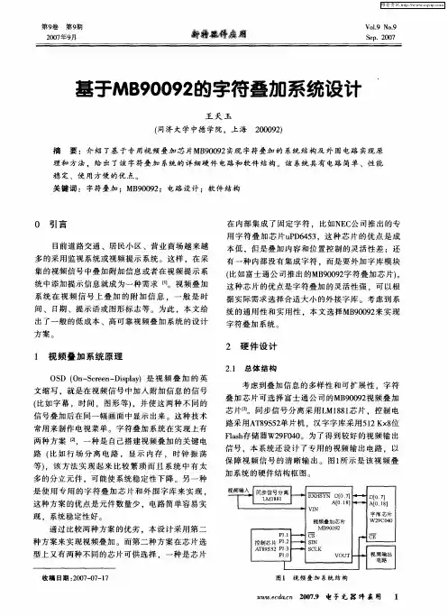
保 障视 频 信 号 的 清 晰输 出。 图 1 所示 是 该 视 频叠
加系统 的硬 件结 构框 图。 阻 输 f步 号 颁 同 信 分离
l
这 种 方案 的优点 是元 件数量 少 。电路简 单 容易 实
现 。系统 稳定性 好 。
I — L l1 l I Mg 8
EHY 0 7 XSND0】 A[8 [ 1
统 的通 用性 和 实用 性 ,本 文选 择 MB o 9 来 实 现 902
间 、 日期 、提 示语 或 图形 标 志等 。为 此 ,本 文给
出 了一般 的低 成本 、高 可靠视 频叠 加 系统 的设 计 方案
字符 叠加 系统 。
2 硬 件 设 计
1 视 频 叠 加 系统 原 理
21 总体 结构 . OS O — cen D sly D f n S re — i a)是 视 频 叠 加 的 英 p
维普资讯
第9 卷
期 2 7第9 0 年月 o 9
婚墓缔 痢
V1 N. o o . 9 9
Sp 0 7 e .2 0
基于MB 0 9 的字符叠加系统设计 902
王 天 玉
( 同济 大 学中德 学院 ,上 海
摘
20 9) 0 0 2
要 :介 绍 了基 于 专 用视 频 叠 加 芯 片 MB 0 9 实现 字 符 叠 加 的 系统 结 构 及 外 围 电路 实现 原 90 2
— VI N
D0】 [7
A[ 1 】 0 8 字库 芯片 W 2 COO 9 4
CE
视 频 叠 加 芯 片
毋9 0 2 0 9
P1 1 CS
通过 比较 两种 方案 的优 劣 。本设 计 采用 第二 种 方案来 实 现视频 叠加 。而第二 种 方案 在芯 片选 型 上又有 两种 不 同的 芯片可 供选 择 。一种 是 芯 片
ANALOG DEVICES AD9520-0 中文数据手册
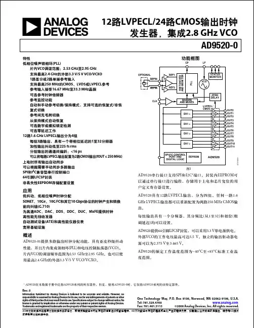
特性 低相位噪声锁相环(PLL) 片内VCO调谐范围:2.53 GHz至2.95 GHz 支持最高2.4 GHz的外部3.3 V/5 V VCO/VCXO 1路差分或2路单端参考输入 支持最高250 MHz的CMOS、LVDS或LVPECL参考 参考输入接受16.67 MHz至33.3 MHz晶振 可选参考时钟倍频器 参考监控功能 自动和手动参考切换/保持模式,支持可选的恢复式/非恢 复式切换 参考间无毛刺切换 从保持模式自动恢复 可选数字或模拟锁定检测 可选零延迟工作 12路1.6 GHz LVPECL输出分为4组 每组3路输出,具有一个带相位延迟的1至32分频器 加性输出抖动低至225 fs rms 分组输出的通道间偏斜:<16 ps 可以将每路LVPECL输出配置为2路CMOS输出(fOUT ≤ 250 MHz) 上电时所有输出自动同步 可以根据需要手动同步多路输出 SPI和I²C兼容型串行控制端口 64引脚LFCSP封装 非易失性EEPROM存储配置设置
DIV/Φ
DIV/Φ
DIV/Φ
图1
AD9520串行接口支持SPI和I2C®端口。封装内EEPROM可 以通过串行接口进行编程,存储用于上电和芯片复位的用 户定义寄存器设置。 AD9520具有12路LVPECL输出,分为四组。任何一路1.6 GHz LVPECL输出都可以重新配置为两路250 MHz CMOS输 出。 每组输出具有一个分频器,其分频比(从1至32)和相位(粗 调延迟)均可以设置。 AD9520提供64引脚LFCSP封装,可以采用3.3 V单电源供电。 外部VCO的工作电压最高可达5.5 V。独立的输出驱动器电 源可以为2.375 V至3.465 V。 AD9520的额定工作温度范围为−40°C至+85°C标准工业温 度范围。
高频耦合防弹芯片数据手册说明书

High Isolation, Silicon SPDT,Nonrefective Switch, 9 kHz to 13.0 GHz Data Sheet HMC1118Rev. 0Document FeedbackInformation furnished by Analog Devices is believed to be accurate and reliable. However, noresponsibility is assumed by Analog Devices for its use, nor for any infringements of patents or other rights of third parties that may result from its use. Specifications subject to change without notice. No license is granted by implication or otherwise under any patent or patent rights of Analog Devices. T rademarks and registered trademarks are the property of their respective owners. One Technology Way, P.O. Box 9106, N orwood, MA 02062-9106, U.S.A. Tel: 781.329.4700 ©2015 Analog Devices, Inc. All rights reserved. Technical Support FEATURESNonreflective 50 Ω designPositive control: 0 V/3.3 VLow insertion loss: 0.68 dB at 8.0 GHzHigh isolation: 48 dB at 8.0 GHzHigh power handling35 dBm through path27 dBm terminated pathHigh linearity1 dB compression (P1dB): 37 dBm typicalInput third-order intercept (IIP3): 62 dBm typicalESD rating: 2 kV human body model (HBM)3 mm × 3 mm, 16-lead LFCSP packageNo low frequency spuriousSettling time (0.05 dB margin of final RF OUT): 7.5 μs APPLICATIONSTest instrumentationMicrowave radios and very small aperture terminals (VSATs) Military radios, radars, and electronic counter measures (ECMs) Fiber optics and broadband telecommunicationsFUNCTIONAL BLOCK DIAGRAMGNDGNDRFCGNDNDNDF1ND12961-1Figure 1.GENERAL DESCRIPTIONThe HMC1118 is a general-purpose, broadband, nonreflective single-pole, double-throw (SPDT) switch in a LFCSP surface mount package. Covering the 9 kHz to 13.0 GHz range, the switch offers high isolation and low insertion loss. The switch features >48 dB isolation, 0.68 dB insertion loss up to 8.0 GHz, and a 7.5 μs settling time of 0.05 dB margin of final RF OUT. The switch operates using positive control voltage logic lines of +3.3 V and 0 V and requires +3.3 V and −2.5 V supplies. The HMC1118 can cover the same operating frequency range with a single positive supply voltage applied and the negative supply voltage (V SS) tied to ground and still maintaining good power handling performance. The HMC1118 is packaged in a 3 mm × 3 mm, surface mount LFCSP package.HMC1118Data SheetRev. 0 | Page 2 of 11TABLE OF CONTENTSFeatures .............................................................................................. 1 Applications ....................................................................................... 1 Functional Block Diagram .............................................................. 1 General Description ......................................................................... 1 Revision History ............................................................................... 2 Specifications ..................................................................................... 3 Electrical Specifications ............................................................... 3 Digital Control Voltages .............................................................. 4 Bias and Supply Current .............................................................. 4 Absolute Maximum Ratings ............................................................ 5 ESD Caution .................................................................................. 5 Pin Configuration and Function Descriptions ..............................6 Interface Schematics .....................................................................6 Typical Performance Characteristics ..............................................7 Insertion Loss, Return Loss, and Isolation ................................7 Input Compression Point and Input Third-Order Intercept ...8 Theory of Operation .........................................................................9 Applications Information .............................................................. 10 Evaluation PCB ........................................................................... 10 Outline Dimensions ....................................................................... 11 Ordering Guide .. (11)REVISION HISTORY10/15—Revision 0: Initial VersionData Sheet HMC1118 SPECIFICATIONSELECTRICAL SPECIFICATIONSV CTRL = 0 V/3.3 V dc, V DD = LS = 3.3 V dc, V SS = −2.5 V dc, T A = 25°C, 50 Ω system, unless otherwise specified.Table 1.Parameter Test Conditions/Comments Min Typ Max Unit INSERTION LOSS9 kHz to 3.0 GHz 0.5 1.0 dB9 kHz to 8.0 GHz 0.68 1.1 dB9 kHz to 10.0 GHz 0.7 1.3 dB9 kHz to 13.0 GHz 1.3 2.0 dB ISOLATION RFC TO RF1/RF2 (WORST CASE)9 kHz to 3.0 GHz 40 50 dB9 kHz to 8.0 GHz 42 48 dB9 kHz to 10.0 GHz 28 35 dB9 kHz to 13.0 GHz 18 25 dB RETURN LOSSOn State 9 kHz to 3.0 GHz 26 dB9 kHz to 8.0 GHz 22 dB9 kHz to 13.0 GHz 9 dB Off State 9 kHz to 3.0 GHz 26 dB9 kHz to 8.0 GHz 14 dB9 kHz to 13.0 GHz 5 dB RADIO FREQUENCY (RF) SETTLING TIME50% V CTRL to 0.05 dB margin of final RF OUT7.5 µs50% V CTRL to 0.1 dB margin of final RF OUT 6 µs SWITCHING SPEEDt RISE/t FALL10%/90% RF 0.85 µst ON/t OFF50% V CTRL to 10%/90% RF 2.7 µs INPUT POWER 1 MHz to 13.0 GHz1 dB Compression (P1dB) 35 37 dBm 0.1 dB Compression (P0.1dB) 35 dBm INPUT THIRD-ORDER INTERCEPT (IIP3) Two-tone input power = 14 dBm at each tone, 1 MHz to 13.0 GHz 62 dBm RECOMMENDED OPERATING CONDITIONS1Positive Supply Voltage (V DD) 3.0 3.6 V Negative Supply Voltage (V SS) −2.75 −2.25 V Control Voltage (V CTRL) Range 0 V DD V Logic Select (LS) Voltage Range 0 V DD V RF Input Power V DD/V CTRL = 3.3 V, V SS = −2.5 V, T A = 85°C, frequency = 2 GHzThrough Path 35 dBm Termination Path 27 dBm Hot Switch Power Level V DD = 3.3 V, T A = 85°C, frequency = 2 GHz 27 dBm Case Temperature Range (T CASE) −40 +85 °C1 These are the recommended values for these parameters.Rev. 0 | Page 3 of 11HMC1118 Data SheetDIGITAL CONTROL VOLTAGESV DD = 3.3 V ± 10%, V SS = −2.5 V ± 10%, T CASE = −40°C to +85°C, unless otherwise specified.Table 2.Parameter Symbol Min Typ Max Unit Test Condition/CommentsINPUT CONTROL VOLTAGE <1 µA typicalLow V IL−0.3 +0.8 VHigh V IH 2.0 V DD + 0.3 VBIAS AND SUPPLY CURRENTTable 3.Parameter Symbol Min Typ Max UnitSUPPLY CURRENTV DD = 3.3 V I DD20 200 µAV SS = −2.5 V I SS0.5 10 µARev. 0 | Page 4 of 11Data SheetHMC1118Rev. 0 | Page 5 of 11ABSOLUTE MAXIMUM RATINGSTable 4.ParameterRatingPositive Supply Voltage (V DD ) Range −0.3 V to +3.7 V dc Negative Supply Voltage (V SS ) Range −2.8 V to +0.3 V Control Voltage (V CTRL ) Range −0.3 V to V DD + 0.3 V Logic Select (LS) Voltage Range−0.3 V to V DD + 0.3 V RF Input Power 1 (V DD /V CTRL = 3.3 V, V SS = −2.5 V, T A = 85°C, Frequency = 2 GHz) See Figure 2 to Figure 4 Through Path 37 dBm Termination Path28 dBm Hot Switch Power Level (V DD = 3.3 V,T A = 85°C, Frequency = 2 GHz) 30 dBm Storage Temperature Range−65°C to +150°C Maximum Reflow Temperature (MSL3 Rating) 260°C Channel Temperature135°C Thermal Resistance (Channel to Package Bottom)Through Path 116°C/W Terminated Path100°C/W ESD Sensitivity (HBM), Class 22 kV1For recommended operating conditions, see Table 1.Stresses at or above those listed under Absolute Maximum Ratings may cause permanent damage to the product. This is a stress rating only; functional operation of the product at these or any other conditions above those indicated in the operational section of this specification is not implied. Operation beyond the maximum operating conditions for extended periods may affect product reliability.4–24–20–16–12–8–40010987654321P O W E R (d B )FREQUENCY (GHz)12961-002Figure 2. Power Derating Through Path4–24–20–16–12–8–400.010.11101001000P O W E R (d B )FREQUENCY (MHz)12961-004Figure 3. Power Derating Through Path (Low Frequency Detail)4–24–20–16–12–8–400.010.1110100100010000P O W E R (d B )FREQUENCY (MHz)12961-003Figure 4. Power Derating for Hot Switching PowerESD CAUTIONHMC1118Data SheetRev. 0 | Page 6 of 11PIN CONFIGURATION AND FUNCTION DESCRIPTIONSDD CTRL SSG N DG N DR F 2G N D G N DG N DR F 1G N D12961-005NOTES1. THE EXPOSED PAD MUST BE CONNECTED TO THE RF/DC GROUND OF THE PRINTED CIRCUIT BOARD (PCB).Figure 5. Pin ConfigurationTable 5. Pin Function DescriptionsPin No.MnemonicDescription1, 2, 4 to 6, 8, 13, 15, 16GNDGround. The package bottom has an exposed metal pad that must connect to the printed circuit board (PCB) RF/dc ground. See Figure 6 for the GND interface schematic.3 RFC RF Common Port. This pin is dc-coupled and matched to 50 Ω. A dc blocking capacitor is required ifthe RF line potential is not equal to 0 V dc.7 RF2 RF2 Port. This pin is dc-coupled and matched to 50 Ω. A dc blocking capacitor is required if the RFline potential is not equal to 0 V dc.14 RF1 RF1 Port. This pin is dc-coupled and matched to 50 Ω. A dc blocking capacitor is required if the RFline potential is not equal to 0 V dc.9 V SS Negative Supply Voltage Pin. 10 V CTRL Control Input Pin. See Table 1, Table 2, and Table 6. 11 LS Logic Select Input Pin. See Table 1, Table 2, and Table 6. 12 V DD Positive Supply Voltage Pin. EPADExposed Pad. The exposed pad must be connected to the RF/dc ground of the printed circuit board (PCB).Table 6. Truth TableControl InputSignal Path StateLS V CTRL RFC to RF1RFC to RF2High L ow On Off High High Off On ow L owOff On ow HighOnOffINTERFACE SCHEMATICSGND12961-006Figure 6. GND Interface SchematicV12961-007V CTRLFigure 7. V CTRL Interface SchematicV 12961-008LSFigure 8. LS Interface SchematicData SheetHMC1118Rev. 0 | Page 7 of 11TYPICAL PERFORMANCE CHARACTERISTICSINSERTION LOSS, RETURN LOSS, AND ISOLATION–4–3–2–12468101214I N S E R T I O N L O S S (d B )FREQUENCY (GHz)12961-009Figure 9. Insertion Loss vs. Frequency–50–40–30–20–10024********R E T U R N L O S S (d B )FREQUENCY (GHz)12961-011Figure 10. Return Loss vs. Frequency0–90–80–70–60–50–40–30–20–102468101214I S O L A T I O N (d B )FREQUENCY (GHz)12961-010Figure 11. Isolation Between RFC and the RF1 and RF2 Ports vs. Frequency0–100–90–80–70–60–50–40–30–20–1002468101214I S O L A T I O N (d B )FREQUENCY (GHz)12961-012Figure 12. Isolation Between RF1 and RF2 Ports vs. FrequencyHMC1118Data SheetRev. 0 | Page 8 of 11INPUT COMPRESSION POINT AND INPUT THIRD-ORDER INTERCEPT4028303234363813121110987654321I N P U T C O M P R E S S I O N (d B m )FREQUENCY (GHz)12961-013Figure 13. 0.1 dB and 1 dB Compression Point vs. Frequency40283032343638013121110987654321I N P U T C O M P R E S S I O N (d B m )FREQUENCY (GHz)12961-014Figure 14. 1 dB Input Compression Point vs. Frequency over Temperature6545505560012108642I N P U T I P 3 (d B m )FREQUENCY (GHz)12961-015Figure 15. Input Third-Order Intercept (IIP3) Point vs. Frequency overTemperature 401015202530350.010.11101001000I N P U T C O M P R E S S I O N (d B m )FREQUENCY (MHz)12961-016Figure 16. 0.1 dB and 1 dB Input Compression Point vs. Frequency(Low Frequency Detail)401015202530350.010.11101001000I N P U T C O M P R E S S I O N (d B m )FREQUENCY (MHz)12961-017Figure 17. 1 dB Input Compression Point vs. Frequency over Temperature(Low Frequency Detail)65605550450.11101001000I N P U T I P 3 (d B m )FREQUENCY (MHz)12961-018Figure 18. Input Third-Order Intercept (IIP3) Point vs. Frequency overTemperature (Low Frequency Detail)Data SheetHMC1118Rev. 0 | Page 9 of 11THEORY OF OPERATIONThe HMC1118 requires a positive supply voltage applied to the V DD pin and a negative supply voltage applied to the V SS pin. Bypassing capacitors are recommended on the supply lines to minimize RF coupling. The HMC1118 can operate with a single positive supply voltage applied to the V DD pin and the negative voltage input pin (V SS ) connected to ground; however, some performance degradations in the input power compression and third-order intercept can occur.The HMC1118 is controlled via two digital control voltages applied to the V CTRL pin and the LS pin. A small value bypassing capacitor is recommended on these digital signal lines to improve the RF signal isolation.The HMC1118 is internally matched to 50 Ω at the RF input port (RFC) and the RF output ports (RF1 and RF2); therefore, no external matching components are required. The RF1 and RF2 pins are dc-coupled, and dc blocking capacitors are required on the RF paths if the RF potential is not equal to a common-mode voltage of 0 V . The design is bidirectional; the input and outputs are interchangeable.The ideal power-up sequence is as follows:1. Power up GND.2. Power up V DD and V SS . The relative order is not important.3. Power up the digital control inputs. The relative order ofthe logic control inputs is not important. Powering the digital control inputs before the V DD supply can inadvertently forward bias and damage the internal ESD protection structures.4. Power up the RF input. The logic select (LS) allows the user to define the control input logic sequence for the RF path selections. With the LS pin set to logic high, the RFC to RF1 path turns on when V CTRL is logic low, and the RFC to RF2 path turns on when V CTRL is logic high. With LS set to logic low, the RFC to RF1 path turns on when V CTRL is logic high, and the RFC to RF2 path turns on when V CTRL is logic low.Depending on the logic level applied to the LS and V CTRL pins, one RF output port (for example, RF1) is set to on mode, by which an insertion loss path provides the input to the output. The other RF output port (for example, RF2) is then set to off mode, by which the output is isolated from the input. When the RF output port (RF1 or RF2) is in isolation mode, internally terminate it to 50 Ω, and the port absorbs the applied RF signal (see Table 7).Table 7. Switch Mode OperationDigital Control Inputs Signal ModeLS V CTRL RFC to RF1 RFC to RF2 High LowOn mode. A low insertion loss path from the RFC port to the RF1 port.Off mode. The RF2 port is isolation from the RFC port andinternally terminated to a 50 Ω load to absorb the applied RF signals.High HighOff mode. The RF1 port is isolation from the RFC port and internally terminated to a 50 Ω load to absorb the applied RF signals.On mode. A low insertion loss path from the RFC port to the RF2 port. Low LowOff mode. The RF1 port is isolation from the RFC port and internally terminated to a 50 Ω load to absorb the applied RF signals.On mode. A low insertion loss path from the RFC port to the RF2 port. Low HighOn mode. A low insertion loss path from the RFC port to the RF1 port.Off mode. The RF2 port is isolation from the RFC port andinternally terminated to a 50 Ω load to absorb the applied RF signals.HMC1118Data SheetRev. 0 | Page 10 of 11APPLICATIONS INFORMATIONEVALUATION PCBGenerate the evaluation PCB used in this application with proper RF circuit design techniques. Signal lines at the RF port must have 50 Ω impedance, and the package ground leads and backside ground slug must be connected directly to the ground plane similarly to what is shown in Figure 19. The evaluation board shown in Figure 19 is available from Analog Devices, Inc. upon request.12961-019Figure 19. EV1HMC1118LP3D Evaluation PCBTable 8. Bill of Materials for the EV1HMC1118LP3D Evaluation Board 1Item Description Manufacturer 2J1 to J3 PC mount SMA RF connectors TP1 to TP5 Through-hole hold mount test points C1, C5 100 pF capacitors, 0402 packageU1 HMC1118 SPDT switch Analog Devices, Inc.PCB 600-01012-00-1 evaluation PCB, Rogers 4350 circuit board materialEV1HMC1118LP3D , Analog Devices, Inc.11 Reference this number to order the full evaluation PCB.2The blank cells in the manufacturer column are left blank intentionally for they are user-selectable.Product OverviewOnlineDocumentation Design ResourcesDiscussionSample & BuyData SheetHMC1118Rev. 0 | Page 11 of 11OUTLINE DIMENSIONS0.080.95FOR PROPER CONNECTION OF THE EXPOSED PAD, REFER TO THE PIN CONFIGURATION AND FUNCTION DESCRIPTIONSSECTION OF THIS DATA SHEET.01-08-2015-A000000*COMPLIANT WITH JEDEC STANDARDS MO-220-VEED-4WITH THE EXCEPTION OF PACKAGE EDGE TO LEAD EDGE.Figure 20. 16-Lead Lead Frame Chip Scale Package [LFCSP_WQ]3 mm × 3 mm Body, Very Very Thin Quad(CP-16-38)Dimensions shown in millimeters1 HMC1118LP3DE and HMC1118LP3DETR are RoHS-Compliant Parts.2See the Absolute Maximum Ratings section. 3XXXX is the 4-digit lot number.©2015 Analog Devices, Inc. All rights reserved. Trademarks and registered trademarks are the property of their respective owners. D12961-0-10/15(0)。
基于MB90092型专用字符叠加电路的视频监控系统的设计与实现

再显示 ,从而检测出被监控方高科技人员随意拆动 监控头系统的行为,有效防止了因信号传输线路被
随意改 动而导 致伪 图像 的 引入 。本系 统能 在一些 要 求 较 高 且 监 视 背
态 伪 随机符 号 的方法 防止系 统在 运行 时监控 头被 拆
卸。 一旦 线路 被拆 动 , 主监控 端给 出 的确认标 识将 不
便使用人员知道该图像信息以何种方式来 自何处及
与之相 关 的信息, 时间, 区徽标 , 时数 据显 示 如 地 实 在 屏幕上 。但是 对 于监 控人 员 而 言 。 控 端遭 到 攻 监 击 是一个 值得担 心 的问题 。因此, 技术方 案 和增 改善 强安 全性 是对 目前状 况提 出 的一 种迫 切要 求 。监 控
t e e a t e so g p e e n r mo e c n r ll O wi e g a a t e . h x cn s fi e a p a d o e t o t O m l b u r n e d ma r o l
Ke wo d : B 0 9 ; vd oc aa trs p rmp st n; mo i rsse ; d sg y rs M 90 2 ie h r ce u ei o i o i nt y tm o ein
a yfo o u p s t c fhg —e h p ro so h emia r nr d c d。 Usn hsmeh d, wa m n p ro eat k o ih tc e sn n te tr n laei t u e r a o ig ti t o
1 引 言
随着监 控现 场 的扩展 和探 头数 量增 多 。 在监 控 端 的图像 显示 系统 中, 常需要 接 收外 部 数据 并 把 经 相 关 的信 息实 时地 连 同 图像 显 示在 监 控屏 幕上 , 以
MB90092 寄存器BIT的含义
Command 3 (VRAM Write Control)FIL : VRAM fill controlFIL = 0:Do not fill VRAM.FIL = 1: Fill VRAM.Command 5 (Screen Control 2)KID : Halftone controlKID = 0 : Perform normal display, disabling halftone display.APC : APC controlAPC = 1 : Turn the APC function ONGYZ : Main screen line enlargement controlBH2 to BH0 : Color phase control Color phase offset 45 degreesW3 to W0 : Main screen line spacing controlCommand 7 (Main Screen Vertical Display Position Control)EC : Sync signal output controlLP : Simple NTSC/PAL controlLP = 0 : Normal operationLP = 1 : Simple NTSC/PAL operationFO : Color phase signal(FSCO pin)output controlY5 to Y0 : Main screen vertical display position control (in dot units)Command 8 (Main Screen Horizontal Display Position Control)SC : Sync signal input control bitSC = 1 : Set the EXHSYN pin as a horizontal sync signal input and the EXVSYN pin as a vertical sync signal input.FC : Sync signal input 3 s filter controlX5 to X0 : Main screen horizontal display position controlCommand 9 (Kanji Font Display Control)GRM : Main screen display mode controlGRM = 0 : Display the main screen in normal mode.The main screen can display only normal characters.The character background color can be set for each character Command 10 (Color Control)RB : Main screen solid-fill background display controlBK : Main screen blink display controlCC : Main screen character color/monochrome controlBC : Main screen character background color/monochrome control(Main screen graphic color/monochrome control)UC : Screen background color/monochrome controlUG, UR, UB : Screen background colorCommand 4 (Screen Control 1)IE : Internal/external synchronization controlIN : Interlaced/noninterlaced display controlEB : Screen background display controlEO : Field controlCM : Color/monochrome display controlZM : Zoom-in controlNP : NTSC/PAL controlNP = 0: Output display signals using the NTSC system.NP = 1: Output display signals using the PAL system.P2, P0 : Pattern background controlDC : Display controlDC = 1: Enable display output operation.Command 0 (VRAM Address Setting)VSL : VRAM write controlRA8 to RA5 : VRAM row address setting (00 to B H)CA4 to CA0 : VRAM column address setting (00 to 17H)Main Screen Sharacter Control Data Write (If VSL = 0 in Command 0)Command 1-1 (Main screen character control data setting 1)Command 2-1 (Main screen character control data setting 2)(MD), MC to M0 : Character codeAT : Specify character attribute display.CG, CR, CB : Character colorsBG, BR, BB : Character background colors(GR) : Specify normal character/graphic character display(BS) : Specify shaded background display.Writing Sub-screen Line Control Data (When Command 0:VSL = 1, CA0 = 0)Set sub-screen line control data.Command 1-2 (Sub-screen line control data setting 1)Command 2-2 (Sub-screen line control data setting 2)SMD to SM0 : Sub-screen line first character codeSDC : Sub-screen line output controlSGR : Sub-screen line character display controlSCG to SCB : Sub-screen line character colors (when SGR = 0)SCG : Sub-screen line graphic color transparency control (when SGR = 1)SCR, SCB : Sub-screen line graphic color phase control (when SGR = 1)Main Screen Line Control Data Write (If VSL = 1 and CA0 = 1in Command 0)This command sets the line control data of the main screen.Command 1-3 (Main screen line control data setting 1)Command 2-3 (Main screen line control data setting 2)OF1, OF0 : Character color phase controlPC : Shaded pattern background color/monochrome controlPG, PR, PB : Shaded pattern background colorG2, G1, G0 : Character size controlSOC : Output priority controlVD : Video signal output controlDG : Digital signal output controlKC : Line background color/monochrome controlKG, KR, KB : Line background colorCommand 11 (Sub-Screen Control)SG2 to SG0 : Sub-screen configuration controlSCC : Sub-screen character color/monochrome controlSBC : Sub-screen character background color/monochrome controlSGC : Sub-screen graphic color/monochrome controlSBG, SBR, SBB : Sub-screen pattern background colorCommand 12 (Sub-Screen Vertical Position Control) SGA : Sub-screen full-screen mode controlSY7 to SY0 : Sub-screen vertical display positionCommand 13 (Sub-Screen Horizontal Position Control) SX8 to SX0 : Sub-screen horizontal display position。
基于MB90092的电梯楼层显示器设计
实现 了将 电梯 当前 所处 楼层相 关信 息动 态实时 叠加 至视频 信号 的功 能 , 时还 能检 测 视频 信 号 的有 无 , 而便 于 保安 监 控人 员 及 时 同 从
处理有 关情 况。应 用结果 表 明 , 系统 运行 稳定 可靠 、 该 编程 简单 、 可维 护性 和可扩 充性 都较 强 。 关键词 :智 能 电磁干扰
状态 ;
⑨ 可 以设置 1 1 ~ 2个字符 的电梯名称 ; ⑩ 自带 国标一 、 二级汉字库。
1 电梯楼 层显 示器 的总体 方案
电梯楼层显 示 器采 用 双 A 8 S2单 片机 作 为 主 T95
要 控 制 芯 片, 与 MB 0 9 、 M18 、 M2 F 8 B 9 0 2 L 8 1 A 9 00 、
和 粤铭 徐 支 影 高 嵩 索 勋 胡 j } l
( 长春理 工 大学 电子信 息工 程学 院 , 吉林 长春 10 2 ) 3 0 2
摘
要 :介绍 了基 于 M 9 0 2型专 用视 频字符 叠加 芯片 的电梯 楼层 显示 器 的硬件 与 软件 设 计 , 合 双 A 8 S 2核 心 的单 片机 系统 , B 09 结 T 95
中图分 类号 :T 2 7 P7
可 靠性
A 8 S 2 频信 号 T9 5 视
动态 实时
安保 监控
文献 标志码 :B
Ab ta t: Had r n ot r e in o i try mo io n ipa ae n MB9 0 2,te d dc td I tx n r p i v rad I sr c r wa ea d s f waed sg fa l soe n tr g d s ly b s d o t f i 09 h e iae C e ta d g a hc o ell C
290 Series Waveform Generators说明书
290 Series Waveform GeneratorsArbitrary WaveformsWaveforms The maximum arbitrary waveform size is 1 M points. Up to 500 user-definedwaveforms may be stored on the removable memory card. Arbitrarywaveforms can be defined by front panel editing controls, by downloading ofwaveform data via RS-232,USB or GPIB, or by writing directly to theremovable memory card using the USB card reader/writer connected to aPC.Waveform memory 1 M points. Minimum waveform size is 8 points.Vertical resolution 12 bitsSample clock range 100 mHz to 100 MHzResolution 4 digitsAccuracy ± 1 digit of settingOutput filter Selectable between 40 MHz Elliptic, 20 MHz Bessel or noneSequence Up to 1024 waveforms may be linked. Each waveform can have a loopcount of up to 32,768. A sequence of waveforms can be looped up to1,048,575 times or run continuously.Noise function Digital noise generated by a 35-bit linear feedback register clocked at 100MHz. User’s external filter defines bandwidth and responseStandard WaveformsWaveforms Sine, square, triangle, DC, positive ramp, negative ramp, sin(x)/x, pulse,pulse train, cosine, haversine and havercosineSine, Cosine, Haversine, HavercosineRange 0.1 mHz to 40 MHzResolution 0.1 mHz or 10 digitsAccuracy Better than 10 ppm for 1 yearTemperature stability Typically < 1 ppm/°COutput level 5 mV to 20 V p-p from 50 ΩHarmonic distortion < 0.15 % THD to 100 kHz; < –60 dBc to 20 kHz, < –50 dBc to 1 MHz, < –40dBc to 10 MHz, < –30 dBc to 40 MHzNon-harmonic spurii < –60 dBc to 1 MHz, < –60 dBc + 6 dB/octave 1 MHz to 40 MHzSquareRange 1 mHz to 50 MHzResolution 1 mHz (4 digits)Accuracy ± 1 digit of settingOutput level 5 mV to 20 V p-p from 50 ΩRise and fall times < 8 nsTriangleRange 0.1 mHz to 500 kHzResolution 0.1 mHz or 10 digitsAccuracy Better than 10 ppm for 1 yearOutput level 5 mV to 20 V p-p from 50 Ω, linearity error: < 0.1 % to 30 kHzRamps and Sin(x)/xRange 0.1 mHz to 500 kHzResolution 0.1 mHz or 10 digitsAccuracy Better than 10 ppm for 1 yearOutput level 5 mV to 20 V p-p from 50 ΩLinearity error < 0.1 % to 30 kHzPulse and Pulse TrainOutput level 5 mV to 20 V p-p from 50 ΩRise and fall times < 8 nsPeriod Range: 40 ns to 100 s; Resolution: 4-digits; Accuracy: ± 1 digit of setting Delay Range: –99.9 s to + 99.99 s; Resolution: 0.001 % of period or 10 nsWidth Range: 10 ns to 99.99 s; Resolution: 0.001 % of period or 10 nsTrains of up to 10 pulses may be specified, each having independently defined width, delay and level. The baseline voltage is separately defined and the sequence repetition rate is set by the pulse train period.Operating ModesContinuous Waveform runs continuouslyTriggered Burst Each active edge of the trigger signal will produce one burst of thewaveformCarrier waveforms All standard and arbitraryMax. carrier frequency The smaller of 2.5 MHz or the maximum for the selected waveform. 100Msamples/s for ARB or Sequence.Number of Cycles 1 to 1048575Trigger rep. rate 0.005 Hz to 100 kHz internal, dc to 1 MHz externalTrigger source Internal from keyboard or trigger generator. External from TRIG IN orremote interface.Start/stop phase ± 360 ° settable with 0.1 ° resolution, subject to waveform frequency andtypeGated Waveform will run while the Gate signal is true and stop while false Carrier waveforms All standard and arbitraryMax. carrier frequency The smaller of 2.5 MHz or the maximum for the selected waveform. 80Msamples/s for ARB or Sequence.Trigger rate 0.005 Hz to 100 kHz internal, dc to 1 MHz externalGate signal source Internal from keyboard or trigger generator. External from TRIG IN orremote interface.Start/stop phase ± 360 ° settable with 0.1 ° resolution, subject to waveform frequency andtypeSweep Capability provided for both standard and arbitrary waveforms.Arbitrary waveforms are expanded or condensed to exactly 4096points and DDS techniques are used to perform the sweep.Carrier waveforms All standard and arbitrary except pulse, pulse train and sequence. Sweepmode: Linear or logarithmic, continuous or triggered.Sweep direction Up, down, up/down or down/upSweep range 1 mHz to 40 MHz in one range. Phase continuous. Independent setting ofstart/stop frequency.Sweep time 1 ms to 999 s (3 digit resolution)Marker Variable during sweep.Sweep trig. Source The sweep may be free run or triggered from the following sources:Manually from keyboard. Externally from TRIG IN input or remote interface. Sweep hold Sweep can be held and restarted by HOLD keyTone Switching Capability provided for both standard and arbitrary waveforms.Arbitrary waveforms are expanded or condensed to exactly 4096points and DDS techniques used to allow instantaneous frequencyswitching.Carrier waveforms All waveforms bar pulse, pulse train, sequenceFrequency list Up to 16 frequencies from 1 mHz to 40 MHzTrigger rep. rate 0.005 Hz to 100 kHz internal, dc to 1 MHz external. Usable repetition rateand waveform frequency depend on the tone switching mode.Source Internal from keyboard or trigger generator. External from TRIG IN orremote interface.Tone switching modesGated The tone is output while the trigger signal is true and stopped, at the end ofthe current waveform cycle, while the trigger signal is false. The next tone isoutput when the trigger signal is true again.Triggered The tone is output when the trigger signal goes true and the next tone isoutput, at the end of the current waveform cycle, when the trigger signalgoes true again.FSK The tone is output when the trigger signal goes true and the next tone isoutput, immediately, when the trigger signal goes true again.External Amplitude ModulationCarrier frequency Entire range for selected waveformCarrier waveforms All standard and arbitrary waveformsModulation source Modulation socketFrequency range DC to 500 kHzSignal range Approx. 1 V pk-pk for 100 % level change at maximum outputExternal Signal SummingCarrier frequency Entire range for selected waveformCarrier waveforms All standard and arbitrary waveformsSum source Sum socketFrequency range DC to 16 MHzSignal range Approximately 2 Vpk-pk input for 20 Vpk-pk output.Trigger GeneratorSource Internal source 0.005 Hz to 100 kHz squarewave adjustable in 10 us steps.3 digit resolution. Available for external use from the SYNC OUT socket. Main Outputs – One for each channelOutput impedance 50 ΩAmplitude 5 mV to 20 V pk-pk open circuit (2.5 mV to 10 V pk-pk into 50 Ω. Amplitudecan be specified open circuit (Hi Z) or into an assumed load of 50 Ωor 60 Ω,in Vpk-pk, Vrms or dBm.Ampl. accuracy Better than 2 % ± 1 mV at 1 kHz into 50 Ω.Ampl. flatness ± 0.2 dB to 1 MHz; ± 0.4 dB to 40 MHzDC offset range ± 10 V. DC offset plus signal peak limited to ± 10 V from 50 Ω. Offset accuracy Typically within ± 3 % ± 10 mV, unattenuatedResolution 3 digits or 1 mV for both Amplitude and DC OffsetSync Out – One for each channel Multifunction output user definable or automatically selected to be any of the following:Waveform sync (All waveforms) A square wave with 50 % duty cycle at the main waveform frequency, or a pulse coincident with the first few points of an arbitrary waveform.Position markers (Arbitrary only) Any point(s) on the waveform may have associated marker bit(s) set high or lowBurst done Produces a pulse coincident with the last cycle of a burstSequence sync Produces a pulse coincident with the end of a waveform sequenceTrigger Selects the current trigger signal. Useful for synchronising burst or gatedsignals.Sweep sync Outputs a pulse at the start of sweep to synchronise an oscilloscope orrecorder. Can additionally output a sweep marker.Phase lock out Used to phase lock two generators. Produces a positive edge at the 0ophase point.Output signal level Logic level of < 0.8 V to > 3 V for all outputs except Sweep Sync. SweepSync is a 3-level waveform.Trig InFrequency range DC to 1 MHzSignal range Threshold nominally TTL level; max. input ± 10 VMin. rulse width 50 ns for Trigger and Gate modes; 50 µs for Sweep modeInput impedance 10 kΩModulation InFrequency range DC to 500 kHzSignal range VCA: Approximately 1 Vpk-pk for 100 % level change at maximum outputSCM: Approximately ± 1 Vpk for maximum outputInput impedance Typically 1 kΩSum InFrequency range DC to 30 MHz (291) DC to 16 MHz (292/294)Signal range Approximately 2 Vpk-pk input for 20 Vpk-pk outputInput impedance Typically 1 kΩHold Holds an arbitrary waveform at its current position. A TTL low level or switchclosure causes the waveform to stop at the current position and wait until aTTL high level or switch opening which allows the waveform to continue.The front panel MAN/HOLD key or remote command may also be used tocontrol the Hold function.Input impedance 10 kΩRef Clock In/OutSet to input Input for an external 10 MHz reference clock. TTL/CMOS threshold level. Set to output Buffered version of the internal 10 MHz clock. Output levels nominally 1 Vand 4 V from 50 Ω.Set to phase lock Used together with SYNC OUT on a master and the TRIG IN on a slave tosynchronize (phase lock) two generators ARB Clock InFrequency Range DC to 50 MHzMax. input voltage + 5 V, -1 VInter-Channel OperationInter-Channel Modulation The waveform from any channel may be used to Amplitude Modulate (AM) or Suppressed Carrier Modulate (SCM) the next channel. Alternatively any number of channels may be Modulated (AM or SCM) with the signal at the MODULATION input socket.Carrier frequency Entire range for selected waveformCarrier waveforms All standard and arbitrary waveformsModulation types AM: Double sideband with carrierSCM: Double sideband suppressed carrierModulation source Internal from the previous channel. External from Modulation input socket.The external modulation signal may be applied to any number of channelssimultaneouslyFrequency range DC to > 100 kHzInternal AM depth 0 % to 105 %Internal AM resolution 1 %Carrier Suppression(SCM)> 40 dBExternal modulation signal range VCA: Approximately 1 V pk-pk for 100 % level change at maximum output SCM: Approximately ± 1 Vpk for max. outputInter-Channel Analogue Summing Waveform Summing sums the waveform from any channel into the next channel. Alternatively any number of channels may be summed with the signal at the SUM input socket.Carrier frequency Entire range for selected waveformCarrier waveforms All standard and arbitrary waveformsSum source Internal from the previous channel. External from SUM IN socket. Frequency range DC to > 16 MHzExt. signal range Approx. 5 Vpk-pk input for 20 Vpk-pk outputInter-Channel Phase Locking Two or more channels may be phase locked together. Each locked channel may be assigned a phase angle relative to the other locked channels. Arbitrary waveforms and waveform sequences may be phase locked but certain constraints apply to waveform lengths and clock frequency ratios.With one channel assigned as the Master and other channels as Slaves a frequency change on the master will be repeated on each slave thus allowing multiphase waveforms at the same frequency to be easily generated. DDS waveforms are those with 7 digits of frequency setting resolution, while Non-DDS waveforms have 4 digits.Phase resolution DDS waveforms: 0.1 degreeNon-DDS waveforms 0.1 degree or 360 degrees/number of points whichever is the greater Phase error < ± 10 ns all waveforms.Inter-Channel Triggering Any channel can be triggered by the previous or next channel. The previous/next connections can be used to ‘daisy chain’ a trigger signal from a ‘start’ channel, through a number of channels in the ‘chain’ to an ‘end’ channel.Each channel receives the trigger out signal from the previous (or next) channel, and drives its selected trigger out to the next (orprevious) channel. The ‘end’ channel trigger out can be set up to drivethe ‘start’ channel, closing the loop.In this way, complex and versatile interchannel trigger schemes maybe set up. Each channel can have its trigger out and its outputwaveform set up independently. Trigger out may be selected fromWaveform End, Position Markers, Sequence Sync or Burst Done.Using the scheme above it is possible to create a sequence of up to 64waveform segments, each channel producing up to 16 segments andall channels being summed to produce the complete waveform at theoutput of channel 4.The signals from the REF IN/OUT socket and the SYNC OUT socketcan be used to phase lock two instruments where more than 4channels are required.InterfacesRS-232 Variable Baud rate, 9600 Baud maximumIEEE488 Conforms with IEEE488.2USB Conforms with USB 1.1General SpecificationsDisplay 20 character x 4 row alphanumeric LCDData entry Keyboard selection of mode, waveform etc.; value entry by numeric keys orby rotary control.Memory card Removable memory card conforming to the Compact Flash memory cardstandard. Sizes from 32 MB to 1 GB can be used.Stored settings Up to 500 complete instrument set-ups may be stored and recalled from thememory card. Up to 500 arbitrary waveforms can also be storedindependent of the instrument settings.Size 130 mm (3U) high; 335 mm long; 350 mm wide (292/294), 212 mm wide(291)Weight 292/294: 7.2 kg (16 lb); 291: 4.1 kg (9 lb)Power 110 to 120 V or 100 V nominal 50/60/400 Hz; 220 to 240 V nominal, 50/60Hz. Voltage adjustable internally; operating range ± 10 % of nominal; 60 VAmax. Installation Category II.ComplianceOperating range +5 °C to 40 °C, 20 to 80 % RHStorage range –20 °C to +60 °CEnvironmental Indoor use at altitudes to 200 m, Pollution Degree 2Safety Complies with EN61010-1EMC Complies with EN61326Instrument drivers Labview and LabWindows CVI drivers are either supplied with theinstrument or are available via your local Fluke OfficeSupplied Items IEC Mains Lead. Printed manual (partly multi-language), multi-languagemanual on CD, Waveform Manager Plus software, compact Flash memorycard, compact Flash card reader/writer (USB connection to PC)Options 19-inch rack mounting kit。
基于OSD控制器MB90092的一种视频安全通信系统设计
20 0 9年 1 2月
苏
州
大
学
学
报( 工
科
版)
V 12 No 6 o. 9 . De . O 9 c2O
J RNAL OF S HOU UNI OU UZ VERST ENGI IY( NEERI NG CI S ENCE EDII T ON)
2 1 电源时钟模 块 .
电路 工作 电压为 5 C, V D 由稳 压芯 片 L85提供 。时钟 模 块 由频 率 为 1MH 和 1.3 MH 的 两无 源 70 2 z 7 744 z 晶振 组成 , 分别 为微控 制模 块 主芯 片 A 8C 1以及 字符 叠加模 块 主芯 片 MB 0 9 T95 90 2提供 工作 时钟频 率 。
2 2 视频 信号 同步分 离模 块 .
视频 信号来 自监 控现 场 的监控摄 像 头 , 占用 带 宽 为 6 5 z 除 图像 信 号外 , 其 . MH , 还包 括 行 场 同步 信 号 、 消 隐信 号 、 脉 冲信号及 前后 均衡 脉 冲等 , 槽 以消 隐 电平 为零 电平 基准 点 。行 、 同步 脉 冲是 字 符显 示 的基 准 , 场 所 以输 入 的视 频 信号 先经 同步分 离 电路 分 离 出行 场 同步脉 冲。视 频 同步 分离 器 采用 N t n l e cn u t 公 ai a S mi d co o o r
全性 能要 求较 高的场合 , 物馆 、 行 、 如博 银 海关 以及公 司仓库等 。
1 系统 工作 原理
视频字 符叠加技 术是 指在 视频上 附着图形或 字符信号 , 从而在屏 幕 的特定位置上 与 图像 信号进行 同时显
示, 这项技术是 应用 电视 技术 中的一个重要 领域 , 应用 电视 系统 中发挥着重 要 的作 用 , 在 现将其 用于视频监 控 系统 , 得视频监 控 、 使 通信更 为安全 可靠 。如 图 1 所示 , 系统在 监控 摄像 头处 附 加 电路 , 用伪 随机 序列 编 本 采 码显示各 种类型 的图形或字 符 , 而远 程监控 中心也采用 与之相对 应 的伪 随机序列 编码来 检测各种类 型 的图形