OSD7556 字符叠加芯片用户手册(V2.1)
OSD7556 字符叠加芯片用户手册
1 = 该行闪烁功能禁止。 0 = 无作用。 N 行显示闪烁使能标志位,该位设 1 表示使能整行的闪烁。 1 = 该行闪烁功能使能。 0 = 无作用。 N 行显示内容清除命令,该位设 1 为清除该行所有显示内容,写 0 到该位无影响。 1 = 将整行内容全部清零。 0 = 无作用
(2)在发送清除屏幕显示内容之后,最大需等待 2 个视频行同步之后(64uS×2)才 能送显示内容进入视频缓冲区,否则有可能清除动作尚未完成而被清除掉该显示内
容。
命令 2:显示移位位置控制
15 – 12 0001
11 10 9 8 7 6 5 4 3 2 1 0 V5 V4 V3 V2 V1 V0 H5 H4 H3 H2 H1 H0
3.3V 电源
功能描述
17.734475MHz 晶体连接
复位端口,低电平有效。 地线, 模拟部分供电电源,3.3V。 内部同步检测用的外部参考电压,外部输入稳定的 0.7V 作为内部同步检测电路参考电压。 同步信号监测的内部比较器输入正向端,可以直接 接入 VIN,或者已经被同步分离器器检测分离出来 的同步信号。 视频信号输入
同步信号输入端
视频信号输入端 No Connected 黑色信号电压输出 No Connected No Connected 场同步输出端口
No Connected No Connected 数字电源地 数字部分电源 SPI 片选信号 SPI 时钟信号 SPI 数据输出端口 SPI 数据输入端口
混合同步输出信号
Bit7-Bit3 Bit2 Bit1 Bit0
缺省值 0010 0000
00 00 0 0
ION 7550_7650用户操作指南_A4(中文版)
用户操作指南北京特域科技有限公司声明:本手册由北京特域科技有限公司翻译,仅供参考之用,所有内容以包装箱内”ION 7550 / ION 7650 Installation Guide”为准。
若有疑问请参考英文版原文,或致电北京特域科技有限公司。
本手册内容如有变更,恕不另行通知。
北京特域科技有限公司ION7550/7650电能质量监控装置用户操作指南目录第一部分:ION 7550 / ION 7650安装指南 (4)安装注意事项 (4)ION7550/ION7650的可选类型 (6)装置的尺寸 (7)第一步:装置的安装 (9)第二步:接地端的连接 (9)第三步:DI/DO和AI/AO的接线 (10)第四步:电压和电流输入的接线 (13)第五步:通信接线 (17)第六步:电源接线 (19)第七步:装置上电 (19)第八步:装置前面板的参数设置 (19)第十步:查看数据 (25)第二部分:ION 7550 / ION 7650面板操作指南 (27)●显示内容的选择 (27)●数值整定 (27)●面板显示内容 (28)●面板设置 (29)●典型接线示意图 (33)●机械安装尺寸 (34)●装置的安装 (35)第一部分:ION 7550 / ION 7650安装指南这种符号表示在装置内或其外壳上存在危险电压,如果不采取适当的预防措施则可能对人体造成电击,重伤或死亡的伤害。
这种符号警告使用者存在危险,如果不采取适当的预防措施则可能对人体造成轻中度伤害,损坏财物或设备本身。
这种符号提示用户注意重要的安装,操作和维护事项。
安装注意事项ION 7550 / ION 7650仪表的安装和维护只能由经过足够的培训,有高电压大电流设备操作经验的合格的工程技术人员来进行。
仪表的安装必须符合当地和国家的电气标准。
如不遵照以下指示可能导致重伤或死亡。
◆在ION 7550 / ION 7650仪表的正常运行中,端子排、电压互感器(PT)、电流互感器(CT)、数字(状态)输入、控制电源和外部I/O回路中都存在危险电压。
DSO5000系列数字存储示波器用户手册(Ver0.9)
DCAT-1008-16产品手册
1) 数码管显示 33 闪动 2) 再按[5],[6]键调节 3) 按[3]键退出或等待 5 秒自动退出 z 按 3 秒按钮 [4]进入调节清晰度模式 1) 数码管显示 44 闪动 2) 再按[5],[6]键调节 3) 按[4]键退出或等待 5 秒自动退出 z 按 3 秒[5]键进入级联端口选择模式 1) 数码管显示 55 闪动 2) 选择一个级联端口后则退出,或等待 5 秒自动退出 z 按 3 秒[6]键初始化各个端口的亮度,清晰度
产品特性:
·单一控制端管理多达 8 台 16 台或 32 台主机 ·可通过两种模式调菜单功能 鼠标右键、热键调 OSD 菜单功能 ·支持密码保护功能 ·超高影像分辨率- 最高达 1600x1200@60Hz ·延长主机与切换器距离-1600*1200@60Hz 分辨率最远可达 50M, 1280*1024@60Hz
通过堆叠串联的方式可从单一控制端最多控制 1024 台服务器 扩展控制端距离:
搭配信号延长器延长控制端距离(如将控制端延伸到机房外操作) 扩展 Over IP 功能:
搭配 IP 模块可实现远程管理,让您不受任何地点限制管理服务器
硬件安装
Cat5 切换器可以堆放在桌面上, 或者安装在机柜的前部或后部,安装前, 请务必 关闭所有要连接的计算机以及外围设备,下面将了解每种安装方式的步骤:
双击鼠标右键或按两次[Scroll Lock], 键盘 LED 指示灯会像跑马灯样闪烁,可访问 以下 OSD 菜单
表 1.4: OSD 界面说明
标题
说明
NO.
主机端口号
ALD7556SBL;ALD7555SAL;ALD7556PBL;ALD7555PAL;中文规格书,Datasheet资料
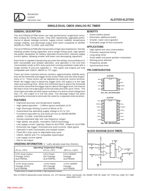
A DVANCED L INEARD EVICES, I NC.SINGLE/DUAL CMOS ANALOG RC TIMERGENERAL DESCRIPTIONThe ALD7555/ALD7556 timers are high performance single/dual mono-lithic analog RC timing circuits. They offer significantly upgraded perfor-mance in speed, leakage currents, supply current, stability, temperature voltage stability, and discharge output drive when compared to SE555/NE555,ICL7555, TLC555, and ICM7555.The ALD7555/ALD7556 offer the benefits of high input impedance, thereby allowing smaller timing capacitors and a longer timing cycle; high speed;low power dissipation for battery operated environment; reduced supply current spikes, allowing smaller and lower cost decoupling capacitors.Each timer is capable of producing accurate time delays and oscillations in both monostable and astable operation, and operates in the one-shot (monostable) mode or 50% duty cycle free running oscillation mode with a single resistor R and one capacitor C. The inputs and outputs are fully compatible with CMOS, NMOS or TTL logic.There are three matched internal resistors (approximately 200K Ω each)that set the threshold and trigger levels at two-thirds and one-third respec-tively of V +. These levels can be adjusted by using the control terminal.When the trigger input is below the trigger level, the output is in the high state and sourcing 2mA. When the threshold input is above the threshold level at the same time the trigger input is above the trigger level, the internal flip-flop is reset, the output goes to the low state and sinks up to 10mA. The reset input overrides all other inputs and when it is active (reset voltage less than 1V), the output is in the low state. The discarge output has been signifcantly enhanced to eliminate the need for a separate external driver.FEATURES•Improved accuracy and temperature stability•High speed operation -- 2.5MHz typical oscillation at 5V •High Discharge Sinking Current of 80mA at 5V•Guaranteed low operating supply voltage of 2V to 10V•Functional equivalent to and same pin-out as NE555/NE556,SE555, TLC555, ICM7555/ICM7556•Greatly expanded high and low frequency ranges •High speed, low power, monolithic CMOS technology•Low supply current, typically: 50µA for ALD7555, 100µA for ALD7556•Extremely low trigger, threshold and reset currents 10pA typical •Operates in both monostable and astable modes •Fixed 50% duty cycle or adjustable duty cycle •CMOS, NMOS and TTL compatible input/output •Low supply current spikes •Rail to rail output•High speed one-shot (monostable)•Precision sequential timing •Long delay timer•Pulse width and pulse position modulation•Missing pulse detector •Frequency divider •Synchronized timer ALD7555/ALD7556BENEFITS•Saves battery power•Eliminates additional buffer •Smaller, lower cost capacitor•Extended range of time constantsAPPLICATIONS* Contact factory for leaded (non-RoHS) or high temperature versions.Operating Temperature Range *0°C to +70°C 0°C to +70°C -55°C to +125°C8-Pin Small Outline 8-Pin Plastic 8-Pin CERDIP Package (SOIC)DIP Package Package ALD7555SAL ALD7555PAL ALD7555DA 14-Pin Small Outline 14-Pin Plastic 14-Pin CERDIP Package (SOIC)DIP Package Package ALD7556SBLALD7556PBLALD7556DBORDERING INFORMATION (“L” suffix denotes lead-free (RoHS))PIN CONFIGURATIONABSOLUTE MAXIMUM RATINGSSupply voltage, V+ 13.2V Input voltage range -0.3V to V+ +0.3V Power dissipation 600 mW Operating temperature range SAL, SBL, PAL, PBL package 0°C to + 70°CDA, DB package-55°C to +125°C Storage temperature range-65°C to +150°C Lead temperature, 10 seconds +260°C OPERATING ELECTRICAL CHARACTERISTICST A= 25o C V+= +5V unless otherwise specifiedParameter Symbol Min Typ Max Unit Test ConditionsSupply Voltage V+210VSupply Current ALD7555I S5090µA Outputs UnloadedSupply Current ALD7556I S100180µATiming error / Astable mode t err 1.0 2.5 % C = 0.1µFInitial AccuracyDrift with Temperature 1∆t/∆T10.0ppm/°C R A = 1KΩDrift with Supply Voltage 1∆t/∆V+0.2%/V R B = 1KΩThreshold Voltage V TH 3.233 3.333 3.433VTrigger Voltage V TRIG 1.567 1.667 1.767VTrigger Current 2I TRIG.010.4nAReset Voltage V RST 0.40.7 1.0VReset Current 2 I RST.010.4nAThreshold Current 2I TH.010.4nAControl Voltage Level V CONT 3.200 3.333 3.467VOutput Voltage Drop (Low)V OL0.20.4V I SINK = 10mAOutput Voltage Drop (High)V OH 4.2 4.6V I SOURCE = -2mARise Time of Output 1t r1030ns R L = 10MΩFall Time of Output 1t f1030ns C L = 10pFDischarge Transistor I DL.0110nALeakage CurrentDischarge Voltage Drop V DISC0.5 1.0V I DISCHARGE = 80mA0.2 0.4V I DISCHARGE = 30mAMaximum Frequency R A = 470ΩAstable Mode f MAX 1.0 2.5MHz R B = 200ΩC T =100pFMinimum Trigger Pulse Width1t TRIG50100nsNotes:1 Sample tested parameters.2 Consists of junction leakage currents with strong temperature dependence.APPLICATION NOTESGENERAL INFORMATIONThe ALD7555 and the ALD7556 devices are analog timers that are, in most situations, direct replacements or direct same pin-out upgrades for the ICM7555, ICM7556, NE/SE555 and NE/SE556 devices. Significantly improved performances for the ALD7555 and the ALD7556 include precision in timing, reduced leakage currents at all the pin terminals, faster switching speeds, reduced switching current spikes, en-hanced discharge output drive currents, better temperature stability, and better timing stability as a function of power supply.These improvements not only improve on the timer function, but also improve on many of the thousands of circuits that depend on this timer architecture, such as modulation cir-cuits, Schmitt triggers, astable circuits, and myriads of mea-surement and control circuits where the user may have reached performance limits with their ICM7555, ICM7556, NE/SE555 and NE/SE556 devices. For a given design, one or more specification of the timer device may become the circuit performance limiting factor. The ALD7555 and the ALD7556 devices are designed to address such limitations and in many cases offer a solution that is simpler and lower cost for a given design challenge than by other solutions by using other circuit means and techniques. ARCHITECTUREThe ALD7555 and the ALD7556 are analog timers that oper-ate based on the RC timing principle, using an external tim-ing resistor R and an external timing capacitor C. The C is charged by the R and then discharged via one of the two output pin connections provided by the ALD7555 and the ALD7556. The control of the two outputs are provided by one of the 4 input pins. The inputs are named THRESH-OLD, CONTROL, RESET and TRIGGER. THRESHOLD and TRIGGER are connected to two separate voltage compara-tors with their respective comparator control levels set by an internal resistor string, consisting of three equal-valued and matched resistors. The output of the two comparators set an internal RS flip-flop circuit, which in turn controls an OUT-PUT and a DISCHARGE output. See Block Diagram for a simplified equivalent circuit. The OUTPUT swings from rail to rail of the supply voltage, whereas the DISCHARGE only sinks current when it is active.The ALD7555 and the ALD7556 operates by charging and discharging the RC timing between 1/3 and 2/3 V+, and by a feedback function provided by the user through the OUT-PUT and/or DISCHAGE pins. This feedback is provided by the application circuit external connections, which determines the mode of the circuit operation. The architecture of this timer takes advantage of the fact that all charging and dis-charging of C are referenced by the reference resistor string that provide reference voltages proportional to supply volt-age V+ (Vdd). As the charging and the discharging of the capacitor C is also proportional to V+, the frequency of os-cillation is independent of V+ voltage levels.The three most basic modes of these external connections are shown as Astable Mode (Free Running Mode), 50% Duty Cycle Mode, and the Monostable Mode. See Typical Appli-cations. There are thousands of application circuits devel-oped that allow the user to manipulate this feedback func-tion, and which then produces many unique functions that is beyond a basic timer function. The application versatility of The ALD7555 and the ALD7556 is only limited by the imagi-nation of the circuit designer.LOW POWER SUPPLY REQUIREMENTSThe CMOS process and the design of the ALD7555 and the ALD7556 devices utilize three well-matched on-chip high impedance resistors to build the internal reference resistor string to provide very low power supply operation. Another technique to achieve low power supply requirement is by using low power MOSFET circuits on-chip, and by allowing the user to use a combination of off-chip timing resistor and capacitor that would reduce their power consumption as well. Generally, this is accomplished by using higher values for R and lower values for C in a combination that would still pro-vide the timing required. Furthermore, reduced on-chip leak-age currents improve on not only timing precision, but also greatly increased ranges of usable R and C values to gener-ate the same RC time constant.ENHANCED DISCHARGE OUTPUT DRIVEThe Discharge Output Drive Currents of the ALD7555 and the ALD7556 devices are increased significantly (80mA) when compared to other timers so that in many applications where the user may use this output as an output driver in-stead of having to add another output driver or buffer cir-cuitry. For example, in many situations, the Discharge Out-put Drive Current is sufficient to drive a relay or a Power MOSFET directly.ASTABLE OPERATIONALD7555 and the ALD7556 devices are designed to func-tion as astable oscillators. These timers can be connected to self trigger and run as a free running mutivibrator. In the free running oscillator mode, the external capacitor C is charged through Ra and Rb, and it is discharged through Rb only. By adjusting the values of Ra and Rb in combination with the value of C, both the frequency and the duty cycle of the oscillator pulse can be adjusted. In the 50% astable mode, the charging and the discharging of C are performed by the same R between the same voltage levels set by the refer-ence resistor string, and therefore timer provide a true 50% duty cycle square wave that is symmetrical. (See typical applications)MONOSTABLE OPERATIONIn this mode of operation the ALD7555 and the ALD7556 can be connected as a one-shot circuit which produces an output pulse with a user-adjustable pulse delay time. The pulse delay time is set by the external R and C values, which together produce a RC time constant that is proportional to the time delay. (See typical applications) The pulse is started with an external negative going Trigger pulse applied to TRIG-GER pin. This negative going pulse set an internal flip-flop so that the external R and C can start the RC timing while the OUTPUT pin is in the HIGH state. The external C is being charged by the external R. When the voltage between the R and C is charged passed the internal threshold volt-age at the THRESHOLD pin, which is set at 66.6% of V+, the internal comparator of the ALD7555 and the ALD7556 resets the internal flip-flop. This then turns on the Discharge Driver at DISCHARGE pin, and discharges the timing ca-pacitor C. The cycle is completed when the OUTPUT is driven to a low state and the ALD7555 and the ALD7556 are again waiting for the next negative going trigger pulse at TRIG-GER pin.CONTROL Voltage and RESET pinsThe CONTROL pin directly accesses one input to the upper comparator. As the input reference resistor string has on-chip high impedance resistors, an input voltage at the CON-TROL input can easily change the voltage at the comparator input. This allows the user to change the oscillation fre-quency, or modulate the oscillation frequency of the analog timer, with a separate user provided frequency. The CON-TROL pin also allows a user-provided inhibit signal to stop and start the timerís oscillation.The RESET terminal directly resets the internal RS flip-flop circuit, which in turn controls the OUTPUT and DISCHARGE pins. This function is activated by a low voltage input of 0.7V of 100 ns minimum duration. By injecting a variety of input signals in a combination to the TRIGGER , THRESHOLD, CONTROL and RESET pins, many interesting modulation and demodulation signals can be manipulated and/or gen-erated by the circuit designer.APPLICATION NOTES (cont’d)TYPICAL PERFORMANCE CHARACTERISTICSTIME DELAY IN THE MONOSTABLE MODEAS A FUNCTION OF R A AND CTIME DELAY 100ns 1µs 1ms 1s 10s C A P A C I T A N C E10 mF100 nF 1 mF100 µF10 µF1 µF 10 nF 1 nF 100 pF10µs 100µs 10ms 100ms 100sSUPPLY CURRENT AS A FUNCTION OFSUPPLY VOLTAGE246810121006050403020100708090SUPPLY VOLTAGE (V)S U P P L Y C U R R E N T (µA )FREQUENCY CHANGE IN THE ASTABLE MODE AS A FUNCTION OF SUPPLY VOLTAGESUPPLY VOLTAGE (V)024612108+4+3+2+10-1-2-3F R E Q U E N C Y C H A N G E (%)-4FREE RUNNING FREQUENCY AS A FUNCTION OF R A , R B AND CFREQUENCY (Hz)1.01K 10K 100K 10M 100M1M 10 mF100 nF C A P A C I T A N C E1 mF 100 µF10 µF 1 µF 10 nF 1 nF 100 pF100.1100D I S CH A R G E S I N K C U R R E N T (m A )DISCHARGE OUTPUT SINK CURRENT AS A FUNCTION OF DISCHARGE LOW VOLTAGEDISCHARGE LOW VOLTAGE (V)0.010.020.050.1 1.00.50.210050205.02.01.00.50.20.110010203040MINIMUM PULSE WIDTH REQUIRED FOR TRIGGERING800600500400300200100 0700LOWEST VOLTAGE LEVEL OF TRIGGERPULSE ( % V + )M I N I M U M P U L S E W I D T H (n s )TYPICAL APPLICATIONS (EACH TIMER)TYPICAL PERFORMANCE CHARACTERISTICS (cont'd)ASTABLE MODE OPERATION50% DUTY CYCLEFrequency f = 1/ (1.4 R C )+ASTABLE MODE OPERATION (FREE RUNNING OSCILLATOR)MONOSTABLE MODE OPERATION (ONE SHOT PULSE)Pulse Delay t d = 1.1 R CµF+Frequency f = 1.46 / (R A + 2R B )C Duty Cycle DC = R B / (R A + 2R B)INPUTµF+O U T P U T S I N K C U R R E N T (m A )OUTPUT SINK CURRENT AS A FUNCTION OF OUTPUT VOLTAGEOUTPUT VOLTAGE (V)0.010.020.050.1 1.00.50.210050205.02.01.00.50.20.110OUTPUT SOURCE CURRENT AS A FUNCTION OF OUTPUT VOLTAGE-1.0-2.0-5.0-10-20-50-0.5-0.5-0.2-0.1-0.05-0.02-0.01-0.2-0.1-1.0OUTPUT VOLTAGE (V)(REFERENCED TO V +)O U T P U T S O U R C E C U R R E N T (m A )8 Pin Plastic SOIC PackageMillimeters InchesMin Max Min Max DimA A1 b C D-8 E e H LS1.750.250.450.255.004.056.300.9378°0.500.0530.0040.0140.0070.1850.1400.2240.0240°0.0100.0690.0100.0180.0100.1960.1600.2480.0378°0.0201.27 BSC0.050 BSC1.350.100.350.184.693.505.700.600°0.25øS (45°)Millimeters Inches Min Max Min Max Dim A A 1b C D-14E eH LS1.750.250.450.258.754.056.300.9378°0.500.0530.0040.0140.0070.3360.1400.2240.0240°0.0100.0690.0100.0180.0100.3450.1600.2480.0378°0.0201.27 BSC 0.050 BSC 1.350.100.350.188.553.505.700.600°0.25ø14 Pin Plastic SOIC PackageS (45°)8 Pin Plastic DIP Package1Millimeters InchesMin Max Min Max DimAA1A2bb1cD-8EE1ee1LS-8ø3.810.381.270.890.380.209.405.597.622.297.372.791.020°5.081.272.031.650.510.3011.687.118.262.797.873.812.0315°0.1050.0150.0500.0350.0150.0080.3700.2200.3000.0900.2900.1100.0400°0.2000.0500.0800.0650.0200.0120.4600.2800.3250.1100.3100.1500.08015°14 Pin Plastic DIP Package1Millimeters InchesMin Max Min Max DimAA1A2bb1cD-14EE1ee1LS-14ø3.810.381.270.890.380.2017.275.597.622.297.372.791.020°5.081.272.031.650.510.3019.307.118.262.797.873.812.0315°0.1050.0150.0500.0350.0150.0080.6800.2200.3000.0900.2900.1100.0400°0.2000.0500.0800.0650.0200.0120.7600.2800.3250.1100.3100.1500.08015°分销商库存信息:ALDALD7556SBL ALD7555SAL ALD7556PBL ALD7555PAL。
科台斯配置工具使用手册_V2.1

注意:
由于产品版本升级或其他原因,本文档内容会不定期进行更新。除非另有约定,本文档仅作为使用指导,本 文档中的所有陈述、信息和建议不构成任何明示或暗示的担保。
关于本文档
作者
CYL
时间
评审
LXJ
时间
签发
时间
2011-2-16 2011-2-16
修改录
文档版本
修改说明
发布日期
作者
签发
2.0
第一次正式发布 2011-2-16 CYL
2.1
修订
2012-3-5
TY
技术支持:021-64136722
第 2 共 10
科台斯无线产品配置工具使用说明书
目录
一.准备...................................................................................................................................................................... 4 二.软件界面说明 ...................................................................................................................................................... 5
网
址:
客户服务电话:
客户服务传真:
客户服务邮箱:
上海市闵行区光华路888号3号楼2层 邮编:201108 021-64136722 021-64136724 support@
OSD视频字符叠加AT7456替换MAX7456
XTAL OSCILLATOR
DAC
Pixels control SAG N ETW O RK OSD GENERATER SAG
CS
, SDOUT to DGND........-0.3V to (V DVDD + 0.3V)
Maximum Continuous Current into V OUT ........................±100mA Continuous Power Dissipation (TA = +70°C) 28-Pin TSSOP (derate 27mW/°C above +70°C).......2162mW* Operating Temperature Range ...........................-40 °C to +85°C Junction Temperature......................................................+150 °C Storage Temperature Range .............................-60 °C to +150°C Lead Temperature (soldering, 10s) .................................+300 °C
杭州中科微电子有限公司
集成了 EEPROM 的 单通道、单色随屏显示器
西门子I755手机使用手册说明书
• Easy subscription to another handset by transferring the memory card
• Blocking of changes to the configuration settings
• Easy (pre-)installation by programming the memory card
User interface
• Icon driven menu
• Status line indicators in the display
• Configurable tricolour LED indicator, e.g., for missed call and • Distinctive melodies for external and internal calls, messages
• Last number redial
Байду номын сангаас
• On-hook number preparation
• Recall/hold (enquiry)
• Silent Charging
• Standby time up to 120 hours
• Talk time up to 10 hours
Design
• Light and ergonomic design
• Dust and (splashing) water proof: IP54
• Inductive charging
• Triple colour LED indication for e.g. missed call and MWI
The DECT handset I755 brings mobile communications for professional DECT users to the highest level: • Anytime, anyplace contact, thus improving customer satisfaction • An excellent communication device with text messaging and alarm information,
FAIRCHILD FDMS7556S 说明书
FDMS7556S N-Channel Power Trench ® SyncFET TMDDDDG SS S® SyncFET TMg FSForward TransconductanceV DS = 5 V, I D = 35 A212S Dynamic CharacteristicsC iss Input Capacitance V DS = 13 V, V GS = 0 V,f = 1 MHz67408965pF C oss Output Capacitance19402580pF C rss Reverse Transfer Capacitance314475pF R gGate Resistance0.61.3ΩSwitching Characteristicst d(on)Turn-On Delay Time V DD = 13 V, I D = 35 A,V GS = 10 V, R GEN = 6 Ω2036ns t r Rise Time918ns t d(off)Turn-Off Delay Time 4877ns t f Fall Time5.311ns Q g Total Gate Charge V GS = 0 V to 10 VV DD = 13 VI D = 35 A 95133nC Q g Total Gate ChargeV GS = 0 V to 4.5 V 4360nC Q gs Gate to Source Gate Charge 18.6nC Q gdGate to Drain “Miller” Charge8.8nCDrain-Source Diode CharacteristicsV SD Source to Drain Diode Forward Voltage V GS = 0 V, I S = 2 A (Note 2)0.370.7V V GS = 0 V, I S = 35 A (Note 2)0.74 1.2t rr Reverse Recovery Time I F = 35 A, di/dt = 300 A/μs4471ns Q rrReverse Recovery Charge68109nCNotes :1. R θJA is determined with the device mounted on a 1in 2 pad 2 oz copper pad on a 1.5 x 1.5 in. board of FR-4 material. R θJC is guaranteed by design while R θCA is determined by the user's board design.2. Pulse Test: Pulse Width < 300 μs, Duty cycle < 2.0%.3. E AS of 312 mJ is based on starting T J = 25 °C, L = 1 mH, I AS = 25 A, V DD = 23 V, V GS = 10 V. 100% test at L = 0.3 mH, I AS = 38 A.4. As an N-ch device, the negative Vgs rating is for low duty cycle pulse occurrence only. No continuous rating is implied.a. 50 °C/W when mounted on a 1 in 2 pad of 2 oz copper.b. 125 °C/W when mounted on a minimum pad of 2 oz copper.TMTMTMTMTMFDMS7556S N-Channel Power Trench ® SyncFET TM*Trademarks of System General Corporation, used under license by Fairchild Semiconductor.DISCLAIMERFAIRCHILD SEMICONDUCTOR RESERVES THE RIGHT TO MAKE CHANGES WITHOUT FURTHER NOTICE TO ANY PRODUCTS HEREIN TO IMPROVE RELIABILITY, FUNCTION, OR DESIGN. FAIRCHILD DOES NOT ASSUME ANY LIABILITY ARISING OUT OF THE APPLICATION OR USE OF ANY PRODUCT OR CIRCUIT DESCRIBED HEREIN; NEITHER DOES IT CONVEY ANY LICENSE UNDER ITS PATENT RIGHTS, NOR THE RIGHTS OF OTHERS. THESE SPECIFICATIONS DO NOT EXPAND THE TERMS OF FAIRCHILD’S WORLDWIDE TERMS AND CONDITIONS, SPECIFICALLY THE WARRANTY THEREIN, WHICH COVERS THESE PRODUCTS.LIFE SUPPORT POLICYFAIRCHILD’S PRODUCTS ARE NOT AUTHORIZED FOR USE AS CRITICAL COMPONENTS IN LIFE SUPPORT DEVICES OR SYSTEMS WITHOUT THE EXPRESS WRITTEN APPROVAL OF FAIRCHILD SEMICONDUCTOR CORPORATION.As used here in:1. Life support devices or systems are devices or systems which, (a) areintended for surgical implant into the body or (b) support or sustain life, and (c) whose failure to perform when properly used in accordance with instructions for use provided in the labeling, can be reasonably expected to result in a significant injury of the user.2.A critical component in any component of a life support, device, or system whose failure to perform can be reasonably expected to cause the failure of the life support device or system, or to affect its safety or effectiveness.PRODUCT STATUS DEFINITIONS Definition of TermsAuto-SPM™Build it Now™CorePLUS™CorePOWER™CROSSVOLT ™CTL™Current Transfer Logic™DEUXPEED ®Dual Cool™EcoSPARK ®EfficentMax™ESBC™Fairchild ®Fairchild Semiconductor ®FACT Quiet Series™FACT ®FAST®FastvCore™FETBench™FlashWriter ® *FPS™FRFET ®Global Power Resource SM Green FPS™Green FPS™ e-Series™G max ™GTO™IntelliMAX™ISOPLANAR™MegaBuck™MICROCOUPLER™MicroFET™MicroPak™MicroPak2™MillerDrive™MotionMax™Motion-SPM™OptiHiT™OPTOLOGIC ®OPTOPLANAR ®®PDP SPM™PowerTrench ®PowerXS™Programmable Active Droop™QFET ®QS™Quiet Series™RapidConfigure™ Saving our world, 1mW/W/kW at a time™SignalWise™SmartMax™SMART START™SPM ®STEALTH™SuperFET™SuperSOT™-3SuperSOT™-6SuperSOT™-8SupreMOS™SyncFET™Sync-Lock™ ®*The Power Franchise ®®TinyBoost™TinyBuck™TinyCalc™TinyLogic ®TINYOPTO™TinyPower™TinyPWM™TinyWire™TriFault Detect™TRUECURRENT™*μSerDes™UHC ®Ultra FRFET™UniFET™VCX™VisualMax™XS™®Datasheet Identification Product Status DefinitionAdvance Information Formative / In Design Datasheet contains the design specifications for product development. Specifications ANTI-COUNTERFEITING POLICYFairchild Semiconductor Corporation’s Anti-Counterfeiting Policy. Fairchild’s Anti-Counterfeiting Policy is also stated on our external website, , under Sales Support .Counterfeiting of semiconductor parts is a growing problem in the industry. All manufactures of semiconductor products are experiencing counterfeiting of their parts. Customers who inadvertently purchase counterfeit parts experience many problems such as loss of brand reputation, substandard performance, failed application, and increased cost of production and manufacturing delays. Fairchild is taking strong measures to protect ourselves and our customers from the proliferation of counterfeit parts. Fairchild strongly encourages customers to purchase Fairchild parts either directly from Fairchild or from Authorized Fairchild Distributors who are listed by country on our web page cited above. Products customers buy either from Fairchild directly or from Authorized Fairchild Distributors are genuine parts, have full traceability, meet Fairchild’s quality standards for handing and storage and provide access to Fairchild’s full range of up-to-date technical and product information. Fairchild and our Authorized Distributors will stand behind all warranties and will appropriately address and warranty issues that may arise. Fairchild will not provide any warranty coverage or other assistance for parts bought from Unauthorized Sources. Fairchild is committed to combat this global problem and encourage our customers to do their part in stopping this practice by buying direct or from authorized distributors.™。
ICP DAS I-7550E 产品说明书
1. IntroductionThis manual introduces the I-7550E's basic setting and operating quickly, the user can refer to the user manual in the ICP DAS companion CD-ROM (Path: “CD:\profibus\converter\i-7550e\manual\i-7550e user manual.pdf”).This manual helps users to understand about the I-7550E module and application. In the following examples the CIF50-PB PROFIBUS Master card from Hilscher is used. The configuration and communication is done by the program “SyCon” provided by Hilscher.Application example of PROFIBUS to Ethernet TCP serverIn this example the I-7550E acts as a TCP Client device. When PROFIBUS Master station sends data, I-7550E module can transfer the data to specific TCP server. If I-7550E module receives the data from TCP server, it can send the data to the input data area of PROFIBUS master station.2. Hardware configurationPower connectionPROFIBUS connectionPROFIBUS connectionHere we recommend users to use the standard PROFIBUS cable and connector (DB9 male). It is only needed to useD-type connector via PROFIBUS cable to connect PROFIBUS Master station and I-7550E module. PROFIBUS Master station and I-7550E module belong to terminalequipments in this example, thus we need to enable the terminator resistor in the D-type connector.Address settingThe I-7550E is a slave device of PROFIBUS DP protocol. The station address of I-7550E can be set by DIP switch. The DIP switch can be seen by open the cover, as shown in the below. The range of DIP switch is 0~126, here we set I-7550E module’s DIP switch to 1.LED status indicatorLEDStatusDescriptionflashWhen PWR led and ERR led are flashing at the same time, which means there is system error in the I-7550E. Please contact us for solution. on Power supply is ok.The firmware has loaded. PWRoff Power supply has failed.flashWhen the I-7550E has diagnostic message, it will flash slowly (flash once about 220ms).on The connection is error with PROFIBUS Master device or PROFIBUS system configuration is not correct. ERRoffPROFIBUS system configuration is correct. It is normal operation. on Data exchange mode. It is normal operation.RUNoffI-7550E module is not in data exchange mode.DIP switch (SW1)Station address 1 2 3 4 5 6 7 81 1 0 0 0 0 0 0 0100 1 0 1 0 0 0 0311 1 1 1 1 0 0 0Note:1=>ON, 0=>OFF3. Establish connection with I-7550EBefore establish the connection between DP-Master and I-7550E, users4. Software configurationGSD filePlease copy the GSD file (IPDS0EB9.gsd) and the bitmap file (i_7550E. bmp, ICP7550E.bmp) from the CD of the I-7550E module into the Profibus configuration tool. File ->CopyGSD(Directory: --> CD:\profibus\converter\i-7550e\gsd\) ¾ the example of how to load GSD fileHere, we use the hilscher CIF50-PB PROFIBUS communication interface to show how to load I-7550E’s GSD file step by step.Step 2: Choose I-7550E device and click Add button.¾Set the modules of the I-7550EThe user needs to set the number and size of the I/O modules in the PROFIBUS configuration tool. The settings of the modules are described below.●Max. I/O modules:32 modules●System setting module:20 Bytes output , 20 Bytes input●Output module:1~16 Bytes, 32Bytes, 64Bytes, 64 Words●Input module:1~16 Bytes, 32Bytes, 64Bytes, 64 WordsIn any case, “System setting module” must be selected first. In this example, we want to have 10 Bytes Input and 10 Byte Output, so we configure a “System setting module”, a “10 Byte In” module and a “10 Byte Out” moduleWhen the user finishes the configuration and saves setting in the PROFIBUS Master station successfully, the 'RUN' LED indicator of I-7550E is turned on. That shows the I-7550E working in the data exchange mode.Click <Online->Download> to download the setting into PROFIBUS Master station¾Set the network configuration of the I-7550E1.Open MiniOS7 utility and press “F12” to find IP address of I-7550E.2.Open web browser (ex. IE). Enter IP address of the I-7550E in theAddress field and press “Enter” to connect to I-7550E, and then enterdefault password (“icpdas”) to login to I-7550E in Login page.3.Click “Server IP Setting” to set the network configuration of the I-7550E (please refer to user manual section 5.3). The networkconfiguration of the I-7550E must have the same domain and differentIP with the PC (ex: PC’s IP=192.168.253.1, MASK=255.255.0.0;andI-7550E’s IP=192.168.253.2, MASK=255.255.0.0).4.Press “Save to Device” to save settings to EEPROM of I-7550E.5.Click “Client IP setting” to set the information of TCP server (pleaserefer to user manual section 5.3). In this case, we setupC_IP9(192.168.253.1) and enable it.6.Press “Save to Device” to save settings to EEPROM of I-7550E andrestart I-7550E.215. I-7550E module communication testThis demo uses TCP server program on the PC to communicate with I-7550E. Users can get it from the ICP DAS companion CDROM(PATH:“CD: \PROFIBUS\Converter\I-7550e\utilities\TCPserver”).The TCPserver setting is shown in the below.TCPserver operate procedure¾ PROFIBUS input/output test--Send data to TCPserver and get response data from TCPserver.The user needs to set the value of “System setting module” from Byte 0~ Byte 10, and set output data (“profibus”) from the Byte 20~ Byte 27. After finishing the setting, the user needs to set the value of Byte 1 from 0 to 1 to trigger the data output function.35Send ''profibus'' string in PROFIBUS output data areaModule Byte Data type RepresentationValue Description Output 0 Byte Hex 0x01 Operation mode Output 1 Byte Hex 0x00→ 0x01Trigger byte Output 2 Byte Hex 0x00Output 3Byte Hex 0x09 Connection ID Output 4 Word Hex 0x00Output 6Word Hex 0x0A Total length of message Output 8Byte Hex 0x01 Total numbers of Index Output 9Byte Hex 0x00 Current Index System moduleOutput 10Byte Hex 0x0A The length of current messageOutput 20Byte Hex 0x70 ‘p’ Output 21Byte Hex 0x72 ‘r’ Output 22Byte Hex 0x6F ‘o’ Output 23Byte Hex 0x66 ‘f’ Output 24Byte Hex 0x69 ‘I’ Output 25Byte Hex 0x62 ‘b’ Output 26Byte Hex 0x75 ‘u’ Output moduleOutput 27ByteHex0x73‘s’At the meantime, TCPserver will response 10 Bytes data “0x00~0x09”. PROFIBUS master can receive data in the input data area, as shown in the below:Receive 10Bytes data(0x00~0x09) in PROFIBUS input data areaModule Byte Data type RepresentationValue Description Input 0 Byte Hex 0x01 Operation mode Input 1 Word Hex 0x00 Message IDInput 3 Word Hex 0x01 Total number of written messageInput 5 Word Hex 0x00 Numbers of message waiting to be write Input 7Word Hex 0x09 Connection ID Input 8 Byte Hex 0x00 Input 9 Word Hex 0x00Input 11 Byte Hex 0x01 Total numbers of Message index Input 12 Byte Hex 0x00 The index of current messageInput 13 Word Hex 0x0A Total length of message System moduleInput 15 Byte Hex 0x0A The length of current messageInput 20 Byte Hex 0x00 Input 21 Byte Hex 0x01 Input 22 Byte Hex 0x02 Input 23Byte Hex 0x03 Input 24 Byte Hex 0x04 Input 25 Byte Hex 0x05 Input 26 Byte Hex 0x06 Input 27 Byte Hex 0x07 Input moduleInput 28ByteHex0x08 Input 29 Byte Hex0x09Received Data from TCPserver ProgramAbout the information of “System setting module”, please refer to user manual Chapter 3 and 4.。
- 1、下载文档前请自行甄别文档内容的完整性,平台不提供额外的编辑、内容补充、找答案等附加服务。
- 2、"仅部分预览"的文档,不可在线预览部分如存在完整性等问题,可反馈申请退款(可完整预览的文档不适用该条件!)。
- 3、如文档侵犯您的权益,请联系客服反馈,我们会尽快为您处理(人工客服工作时间:9:00-18:30)。
命令 3:字符整行控制命令
15 – 12 11 10 9 8 7 6 5 4 3
2
1
0
0010
R3 R2 R1 R0
BLK_OFF BLK_ON CLR
位域 Bit15-Bit12 Bit11-Bit8
Bit7-Bit3 Bit2
缺省值 0010 0000
00 00
功能描述 命令码 行号值,0000 = 字符显示行 1。
1 = 该行闪烁功能禁止。 0 = 无作用。
7 / 31
Bit1
0
N 行显示闪烁使能标志位,该位设 1 表示使能整行的闪烁。
1 = 该行闪烁功能使能。
0 = 无作用。
Bit0
0
N 行显示内容清除命令,该位设 1 为清除该行所有显示内容,写 0
到该位无影响。
1 = 将整行内容全部清零。
0 = 无作用
20
VL2
21
NC
No Connected
22
NC
No Connected
23
VSS
数字电源地
24
VDD 数字部分电源
25
CS
SPI 片选信号
3.3V SPI 通信接口
26
SCLK SPI 时钟信号
27 SDOUT SPI 数据输出端口
28
SDIN SPI 数据输入端口
29
NC
30
NC
31
NC
32 HSYNC 混合同步输出信号 同步信号比较器的同步输出,如果 SYNC_IN 直连到 VIN 的话,则从该脚可以检测到同步信号比较器检 测到同步信号的质量,从而调整 SYNC_REF 得到最 佳的同步检测效果。
= 1,每一次写 VRAM 数据之后,VRAM 地址自动递增加 1。 = 0,每一次写 VRAM 数据之后,VRAM 地址不变。 Reserved VRAM 地址,VRAM 地址超出显示范围,则直接忽略该命令。 VRAM 地址设定请参考下面的图所示
显示内存区域(VRAM)示意图 0 24 …… Display Area (12 Rows × 24 Characters) ……
9
VDDA 模拟部分电源
模拟部分供电电源,3.3V。
10 SYNC_REF 同步检测参考电压 内部同步检测用的外部参考电压,外部输入稳定的
0.7V 作为内部同步检测电路参考电压。
11 SYNC_IN 同步信号输入端 同步信号监测的内部比较器输入正向端,可以直接
接入 VIN,或者已经被同步分离器器检测分离出来
Bit11-Bit8 00000 Reserved
Bit7
0
VRAM 清理操作,1 = 将所有的显示内存 VRAM 全部清 0,该位硬件
自动清零,写 0 到该位无影响。
Bit6
0
字符闪烁基准时间设定(BT),每一个基准时间后,闪烁状态进行翻
转一次。占空比固定为 50:50。 0 = 0.5 秒。
1 = 1 秒。
OSD7556 具有唯一 ID 码的 24 点阵汉字字符叠加芯片 用户手册
(版本:V2.1)
版本修改说明:
序号 1 2 3
修改说明 开放内同步背景灰度寄存器设置(命令 8) 修改应用线路图和 BOM 表 删除控制命令 1 的 bit1 功能说明,PAL/NTSC 制式自动兼容。
参考页面 P11 P20-P21 P6
264
23
Line 0
47
Line 1
287 Line 11
命令 5:显示存储器(VRAM)字符设定
15 – 12 0100
11 10 9 8 7 6 5 4 3 2 1 0 BL A1 A0 C8 C7 C6 C5 C4 C3 C2 C1 C0
位域 Bit15-Bit12
Bit11
缺省值 0100
Vdd-Vss
外部供电电压
-0.3
4
Vspi-Vss
通信数据线耐受电压
-0.3
5.5
Twork
工作温度
-40
85
Tstg
储存温度
-40
150
注意:不要超出上表所列的环境条件,否则芯片可能无法正常工作甚至受损坏。
单位 V V ℃ ℃
2 / 31
工作特性
符号 Vdd Vspih Vspil Fclk VIN Iopr
描述 电源电压 SPI 数字信号输入高电平 SPI 数字信号输入低电平 时钟频率 视频输入信号 工作电流
管脚图
最低 标准 最高
+3.0 +3.3 +3.6
+2.7
+5.0
+0.8
17.734475
0.5
1.2
50 100
单位 V V V
MHz Vp-p mA
管脚功能描述
序号 1 2
标注 VDD NC
0
命令码 字符属性闪烁位
功能描述
8 / 31
Bit10-Bit9 Bit8-Bit0
1 = 该字符闪烁显示功能打开 0 = 该字符闪烁显示功能关闭 00 VRAM 字符地址的分区码,OSD 芯片中共分有 4 个区域存储字符点阵, 第 1 区为固化在芯片内部空间的 96 个半角字符,第 2 区为用户定制 在 RAM 中的 64 个半角字符,第 3 区包括固化在芯片内部的 384 个 全角字符的第一部分,第 4 区包括固化在芯片内部的 384 个全角字 符的第二部分。全角字符的显示是将同地址的第 3 区的第一部分同 第 4 区的第二部分组合在一起显示。 A1,A0 00 = 第 1 区(芯片内置半角字符),C7 为无效位,C6-C0 为 96 个相应的有效字符点阵数据地址。 01 = 第 2 区(RAM 区字符),C7,C6 为无效,C5-C0 为有效的 字符点阵数据地址。 10 = 第 3 区(全角字符的第一个显示位置),C8-C0 为 384 个相 对应的点阵数据地址。 11 = 第 4 区(全角字符的第二个显示位置),C8-C0 为 384 个相对应 的点阵数据地址。
注意:(1)Bit8 相当于清除屏幕显示内容,而显示控制方式并不发生变化;Bit3 是相当于芯
片复位,不仅清除屏幕显示内容,而且所有的控制寄存器会初始化成缺省值。
6 / 31
(2)在发送清除屏幕显示内容之后,最大需等待 2 个视频行同步之后(64uS×2)才 能送显示内容进入视频缓冲区,否则有可能清除动作尚未完成而被清除掉该显示内容。
VRAM 字符地址(C8-C0),其中如果 A1A0 为 00 的话,则 C8C7 为无 效位,芯片将忽略该两位。A1A0 为 01 的话,则 C8C7C6 为无效位, 芯片将忽略该 3 位。A1A0 为 10 或 11 时,该 C8-C0 全为有效地址位。
全角汉字显示说明: 本芯片内置 384 个全角汉字点阵(可以由厂家生产时定制),每一个全角汉字包括两个基本 显示位置(12×18 点阵),每个汉字相对应的具有 24×18 点阵数据,在内部相对应的将两 个基本位置分别放在两个不同区域,在两个区域里面的同一个位置(0x000-0x17F)对应同 一个汉字的两个显示位置。 图 2: 一个 24×18 的全角汉字显示点阵如下:
000001 = 9H + 1 000010 = 9H + 2 ………………… 111111 = 9H + 63 水平位置寄存器,起始位置为每行的 12us 处开始,每一个移位单 位为 2/Fclk, 000000 = 12uS + 0 * 2/Fclk 000001 = 12uS + 1 * 2/Fclk 000010 = 12uS + 2 * 2/Fclk ……………………………… 111111 = 12uS + 64 * 2/Fclk
0001 = 字符显示行 2。 0010 = 字符显示行 3。 0011 = 字符显示行 4。 ………………………… 1111 = 字符显示行 16。 OSD 芯片最多支持 12 行显示,所以行号超出所规定范围之后的命 令将被直接忽略。
Reserved N 行显示闪烁禁止标志位,该位设 1 表示禁止该行的闪烁功能。
版本 V2.0 V2.0 V2.1
1 / 31
特性
★ 支持标准的英文半角字符显示(12×18)和全角的 24 点阵汉字字符显示(24×18) 的混合显示。
★ 内置字符共支持 96 个半角字符和 384 个全角字符,通过专用字符生成工具可在生 产时由用户定制所需的字符及其自定义图标等。
★ RAM 可实时更改字符共 64 个半角字符(32 个 24 点阵汉字),提供专用的字符点阵 生成软件,不存在 RAM 字符字体和内置字体不一致的问题。
命令 2:显示移位位置控制
15 – 12 0001
11 10 9 8 7 6 5 4 3 2 1 0 V5 V4 V3 V2 V1 V0 H5 H4 H3 H2 H1 H0
位域 Bit15-Bit12 Bit11-Bit6
Bit5-Bit0
缺省值 0001 001000
001000
功能描述 命令码 垂直位置寄存器,起始位置为场同步后第 9 行开始,最大位移为 64 行, 000000 = 9H + 0
★ 可单独设定每一个显示单位(12×18)闪烁功能。 ★ 最多可显示 12 行×24 列标准显示单位,如果全部为汉字的话,最多可显示 12 行×
12 列的全角汉字。 ★ 内置视频信号同步发生器,内部、外部视频同步信号自动切换。 ★ SPI 兼容串行通信接口,最大通信速率达 10MHz。单一 16bit 指令格式,控制简单方
命令 4:显示存储器(VRAM)地址设定
15 – 12 0011
11 10 9 8 7 6 5 4 3 2 1 0