TFT触摸屏使用说明
MY-TFT070V2产品用户手册说明书
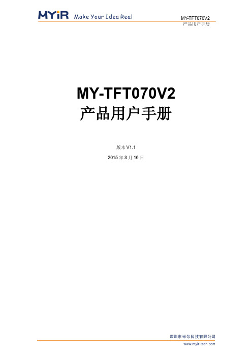
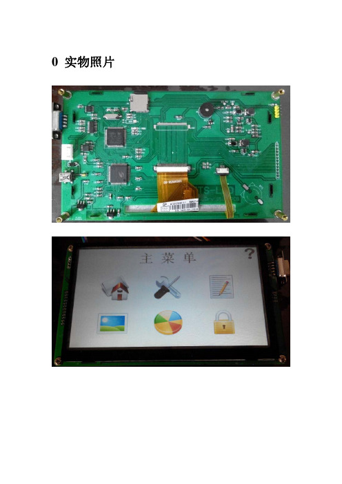
MY-TFT070V2 产品用户手册版本V1.12015年3月16日版本记录目录目录 (1)第1章产品概述 (2)1.1 产品简介 (2)1.2 规格参数 (2)1.3 产品预览 (3)第2章硬件指南 (5)2.1 引脚分布 (5)2.2 信号定义 (5)2.3 电气特性 (6)2.4 时序参数 (7)第3章机械参数 (10)附录 (12)附录一联系方式 (13)附录二售后服务与技术支持 (14)第1章产品概述1.1 产品简介MY-TFT070V2是深圳米尔科技有限公司推出的7寸液晶模块,是彩色有源矩阵薄膜晶体管(TFT)液晶显示器(LCD),由TFT LCD显示器件,连接件,控制与驱动外围电路,PCB驱动底板等组成,驱动底板预留1.27mm间距的IDC排线插针(25pinX2)和0.5mm 间距的FPC连接器两种连接方式,是专为米尔科技ARM主板设计的配套LCD液晶显示模块。
1.2 产品特性MY-TFT070V2兼容三种触摸输入方式,分别为电阻式触摸输入、电容式触摸输入和外置式输入,可以根据需要任意选用需要的方式,同时只能有一种触摸方式被连接。
图1-1MY-TFT070V2带有一颗存储芯片,用来保存LCD的一些常规信息,MYiR的开发板系统能够版识别MY-TFT070V2,并根据这些信息来加载相应的驱动。
1.3 规格参数1.4 产品预览MY-TFT070V2 产品平面图如图1-2、图1-3所示:图1-2 MY-TFT070V2产品正面图图1-3 MY-TFT070V2 产品背面图第2章硬件指南2.1 接口分布底板接口分布如下图2-1所示:图2-1 底板接口分布图如上图所示,驱动底板预留1.27mm间距的50pin IDC排线插针(J1)和0.5mm间距的50pin FPC连接器(J2)两种连接方式,默认连接50pin IDC排线。
J4为电阻触摸信号连接,J5,J7分别为电容触摸控制信号连接,默认选择J5电容触摸模式。
TTS-LCD串口TFT显示屏使用说明
1 硬件接口说明
1.1 LCD70
电源输入 5V RS口 IO 扩展接口
Mini USB 电 源输入 5V
电源输入 5V RS485 接口
说明: 电源:单电源 5V 输入,可通过 USB、RS232、RS485 接口输入 通信接口:RS232、RS485 公用 STM32 USART1,PA11 控制 485 发送接收,1 发送 0
//----------------------------------------------------------------------------------------//填充圆形 圆心(x0,y0) 半径 r 颜色 color
//-----------------------------------------------------------------------------------------
extern void GUI_RectangleFill(u16 x0, u16 y0, u16 x1, u16 y1, TCOLOR color);
//-----------------------------------------------------------------------------------------
//----------------------------------------------------------------------------------------//输出字符串 ASCII
//x
起点 x 轴坐标值
//y
起点 y 轴坐标值
//size
16(8*16) 24(12*24) 32(16*32) 48(24*48) 64(32*64)
1.77寸TFT使用说明
1.77寸TFT使用说明外观美观大方,质量可靠,采用品牌厂商生产的TFT,提供多个例程,程序精炼、准确、实用。
您的满意就是我们的成功!TFT尺寸:1.7”;分辨率:128xBGRx160,可达262K色;电压类型:支持5V或3.3V电压输入,5v电压接入时,“VCC_SEL”(即16、17pin)断开;3.3v电压接入时,“VCC_SEL”短接;接口类型:支持8位数据接口或16位数据接口,8位数据接口可与12864液晶接口兼容(修改一下程序中的接口定义即可)。
使用16位数据接口时,“MOD”(即18pin)连接到GND。
兼容12864接口,TFT第一脚与12864接口第一脚对齐,注意12864接口的背光控制脚(第三脚)用跳帽连接到地(使TFT的CS控制信号为低电平)如果TFT仍显示不了则需将12864接口电位器旋转至GND。
TFT液晶各引脚功能说明如下:GND:接地;VCC:5V/3V电压输入,注意VCC_SEL的连接;CS:片选信号;RS:命令/数据选择;RS=0写数据,RS=1写命令;WR:写控制信号;RD:读控制信号;D8~D15: 使用8位数据口时为8位数据/命令并行口;使用16位数据/命令并行口时为其高8位;RST:液晶复位信号;VCC_SEL: 5v VCC接入时“VCC_SEL”断开;3.3v VCC接入时“VCC_SEL”短接;MOD: 数据/命令并行口的模式选择,MOD=GND时TFT为16位工作模式,MOD 不连接时TFT为8位工作模式;D0~D7:仅在使用16位数据/命令并行口时使用,为16位数据/命令并行口的低8位;液晶控制IC说明请参考“S6D0144.pdf”,液晶FPC接口定义请参考“GG1P0360管脚定义.pdf”。
8位接口模式,程序中的接口定义:D8~D15 = P0;CS = P2^1;RST = P2^2;RS = P2^5;WR_ = P2^4;RD_ = P2^3;16位接口模式,程序中的接口定义:D0~D7 = P0;D8~D15 = P1;CS = P2^1;RST = P2^2;RS = P2^5;WR_ = P2^4;RD_ = P2^3;SD卡使用方法程序4的功能是将SD卡中存储的图片显示到TFT,故此处SD卡主要用来存储图片。
Riverdi 3.5英寸 TFT 显示屏参考手册说明书

ITEMCONTENTSUNITLCD Type TFT/Transmissive/Normally white / Size3.5Inch Viewing Direction12:00 (without image inversion) O’ Clock Gray Scale Inversion Direction 6:00O’ Clock Number of Dots 320 x (RGB) × 240 / Driver ICBT81x / Interface TypeSPI/QSPI/ Module Memory Size 1 MB (BT81x) + 64 Mb (external flash) / Color Depth16.7M/ Pixel Arrangement RGB Vertical Stripe/ Surface Treatment Anti-glare / Clear (for CTP) / Input Voltage3.3V3.5” EVE3 SERIES LCD TFTRiTFT-35 seriesRev.1.0 2018-10-22L C D T F T M o d u l e S p e c i f i c a t i o nNote 1: RoHS, REACH SVHC compliant Note 2: LCM weight tolerance: ± 5%.CONTENTS (2)1 MODULE CLASSIFICATION INFORMATION (3)2 ASSEMBLY GUIDE - INTEGRATION (3)2.1 Mounting frame (4)3 MODULE DRAWING (4)4 ABSOLUTE MAXIMUM RATINGS (5)5 ELECTRICAL CHARACTERISTICS (5)6 BACKLIGHT CHARACTERISTICS (5)7 ELECTRO-OPTICAL CHARACTERISTICS (5)8 INTERFACE DESCRIPTION (7)9 BT8x CONTROLLER SPECIFICATIONS (8)9.1 Serial host interface (8)9.2 Block Diagram (8)9.3 Host interface SPI mode 0 (9)9.4 Backlight driver block diagram (9)10 LCD TIMING CHARACTERISTICS (9)10.1 Clock and data input time diagram (9)10.2 Parallel RGB timing table (11)11 TOUCH SCREEN PANEL SPECIFICATIONS (11)11.1 Electrical characteristics (11)11.1.1 For capacitive touch panel (11)11.1.2 For resistive touch panel (12)11.2 Mechanical characteristics (12)11.2.1 For capacitive touch panel (12)11.2.2 For resistive touch panel (13)12 INSPECTION (13)12.1 Inspection condition (13)12.2 Inspection standard (14)13 RELIABILITY TEST (17)14 LEGAL INFORMATION (18)1. BRAND RV – Riverdi2. PRODUCT TYPE T – TFT StandardF – TFT Custom3. DISPLAY SIZE 35– 3.5”4. MODEL SERIAL NO. A (A-Z)5. RESOLUTION H– 320x240 px6. INTERFACE B – TFT + Controller BT81x7. FRAME N – No FrameF – Mounting Frame8. BACKLIGHT TYPE W – LED White9. TOUCH PANEL N – No Touch PanelR – Resistive Touch Panel C – Capacitive Touch Panel10. VERSION 00(00-99)RiTFT-35-RES RVT35AHBNWR00 BT816, resistive touch panelRiTFT-35-CAP RVT35AHBNWC00 BT815, capacitive touch panelRiTFT-35-FR RVT35AHBFWN00 BT816, no touch panel, mounting frame RiTFT-35-RES-FR RVT35AHBFWR00 BT816, resistive touch panel, mounting frame RiTFT-35-CAP-FR RVT35AHBFWC00 BT815, capacitive touch panel, mounting frame2.1Mounting frameFor dimension s 3.5”, 4.3”, 5.0” and 7.0” the product with mounting frame version is available. Thanks to the four catches attached to the side, frame provides strong assembly to the surface by mounting element (like the screw, see Figure 3). The frames are specially designed to fit Riverdi products perfectly. The diameter of the mounting hole is 3.5mm.Figure 1. Mounting frameRiTFT-35 series3MODULE DRAWING `` RiTFT-35© 2018 Riverdi Page 4 of 24 RiTFT-35 seriesRiTFT-35-FR© 2018 Riverdi Page 5 of 24 RiTFT-35 seriesRiTFT-35-CAP© 2018 Riverdi Page 6 of 24 RiTFT-35-CAP-FR© 2018 Riverdi Page 7 of 24 RiTFT-35-RES© 2018 Riverdi Page 8 of 24 RiTFT-35-RES-FR© 2018 Riverdi Page 9 of 24 4ABSOLUTE MAXIMUM RATINGSPARAMETER SYMBOL MIN MAX UNITSupply Voltage for Logic VDD 0 4.0 V Supply Voltage for LED Inverter BLVDD 0 7.0 VInput Voltage for Logic VIN 0 4.0 VLED forward current (each LED) IF - 25 mA Operating Temperature T OP-20 70 °C PARAMETER SYMBOL MIN TYP MAX UNIT NOTES Supply Voltage For Module VDD 3.0 3.3 3.6 VInput Voltage for LED Inverter BLVDD 2.8 5.0 5.5 VLED Backlight Current IDD backlight- 150 187 mA BLVDD=3.3V LED Backlight Current IDD backlight- 93 117 mA BLVDD=5V Input Voltage ' H ' level V IH0.7VDD - VDD VInput Voltage ' L ' level V IL0 - 0.2VDD VInput Current I In TBD mAInput Current for module with CTP I InC TBD mAITEM SYMBOL MIN TYP MAX UNIT Voltage for LED backlight V l- 19.2 20.4 V Current for LED backlight I l- 20 25 mA LED Life Time - 30000 50000 - HrsLNote 1. Contrast Ratio(CR) is defined mathematically as below, for more information see Figure .Contrast Ratio =Average Surface Luminance with all white pixels (P1,P2,P3,P4,P5) Average Surface Luminance with all black pixels (P1,P2,P3,P4,P5)Note 2. Surface luminance is the LCD surface from the surface with all pixels displaying white. For more information, see Figure .Lv = Average Surface Luminance with all white pixels (P1, P2, P3, P4, P5)Note 3.The uniformity in surface luminance δ WHITE is determined by measuring luminance at each test position 1 through 5, and then dividing the maximum luminance of 5 points luminance by minimum luminance of 5 points luminance. For more information, see Figure .δ WHITE =Minimum Surface Luminance with all white pixels (P1,P2,P3,P4,P5) Maximum Surface Luminance with all white pixels (P1,P2,P3,P4,P5)Note 4. Response time is the time required for the display to transition from white to black (Rise Time, Tr) and from black to white (Decay Time, Tf). For additional information see FIG 1. The test equipment is Autronic-Melchers’s ConoScope series.Note 5.CIE (x, y) chromaticity, the x, y value is determined by measuring luminance at each test position 1 through 5, and then make average value.Note 6. Viewing angle is the angle at which the contrast ratio is greater than 2. For TFT module the contrast ratio is greater than 10. The angles are determined for the horizontal or x axis and the vertical or y axis with respect to the z axis which is normal to the LCD surface. For more information see Figure .Note 7. For viewing angle and response time testing, the testing data is based on Autronic-Melchers’s ConoScope series. Instruments for Contrast Ratio, Surface Luminance, Luminance Uniformity, CIE the test data is based on TOPCON’s BM-5 photo detector.Note 8. For TFT module, Gray scale reverse occurs in the direction of panel viewing angle.Figure 2. The definition of response timeFigure 3. Measuring method for Contrast ratio, surface luminance, Luminance uniformity, CIE (x, y) chromaticityFigure 4.The definition of viewing angle8INTERFACE DESCRIPTION9BT8x CONTROLLER SPECIFICATIONSBT8x or EVE3 (Embedded Video Engine 3) simplifies the system architecture for advanced human machine interfaces (HMIs) by providing functionality for display, audio, and touch as well as an object oriented architecture approach that extends from display creation to the rendering of the graphics.9.1Serial host interfaceFigure 5.SPI interface connection Figure 6. QSPI interface connectionSPI Interface– the SPI slave interface operates up to 30MHz.Only SPI mode 0 is supported. The SPI interface is selected by default (MODE pin is internally pulled low by 47k resistor).9.2Block DiagramFigure 7.. BT8x Block diagram9.3Host interface SPI mode 0Figure 8. SPI timing diagramFor more information about BT8x controller please go to official BT8x website.https:///Products/ICs/BT81X.html9.4Backlight driver block diagramBacklight enable signal is internally connected to BT8x Backlight control pin. This pin is controlled by two BT8x’s registers. One of them specifies the PWM output frequency, second one specifies the duty cycle. Refer to BT8x datasheet for more information.Figure 9. Backlight driver block diagram10LCD TIMING CHARACTERISTICS10.1Clock and data input time diagramFigure 10. DE mode timing diagramBT8xFigure 11. SYNC mode timing diagramFigure 12. Timing diagram10.2Parallel RGB timing tableTiming parameter (VDD=3.3V, GND=0V, Ta=25˚C)PARAMETER SYMBOL MIN TYP MAX UNIT CONDITION CLK Clock Time T clk 1/Max(F CLK) - 1/Min(F CLK) ns -11TOUCH SCREEN PANEL SPECIFICATIONS11.1Electrical characteristicsNote: Avoid operating with hard or sharp material such as a ball point pen or a mechanical pencil except a polyacetal pen (tip R0.8mm or less) or a fingerITEM VALUE UNIT REMARKMin. Typ. Max.Linearity - - 1.5 % Analog X and Y directions Terminal Resistance 200 - 900 ΩX100 - 600 ΩY11.2Mechanical characteristicsNote 1: Force test condition, Input DC 5V on X direction, Drop off Polyacetal Stylus (R0.8), until output voltage stabilize, then get the R8.0mm Silicon rubber and do finger Activation force test. Next step, 9 points.Note 2: Measurement surface area conditions, Scratch 100,000 times straight line on the film with a stylus change every 20,000 times with Force: 250gf, Speed: 60mm/sec by R0.8 polaceteal stylus.Note 3: Pitting test, Pit 1, 000, 000 times on the film with R0.8 silicon rubber with Force: 250gf and Speed: 2 times/sec.Note 1: Force test condition, Input DC 5V on X direction, drop off Polyacetal Stylus (R0.8), until output voltage stabilize, then get the R8.0mm Silicon rubber and do finger Activation force test. Next step, 9 points.ITEM VALUE UNIT REMARKMin. Typ. Max.12INSPECTIONStandard acceptance/rejection criteria for TFT module.12.1Inspection conditionAmbient conditions:•Temperature: 25±°C•Humidity: (60±10) %RH•Illumination: Single fluorescent lamp non-directive (300 to 700 lux)Viewing distance:35±5cm between inspector bare eye and LCD.Viewing Angle:U/D: 45°/45°, L/R 45°/45°12.2Inspection standard Item Criterion Black spots, whitespots, light leakage,Foreign Particle(round Type)D=(x+y)2*Spots density: 10 mmSize < 5”Average Diameter Qualified QtyD < 0.2 mm Ignored0.2 mm < D < 0.3 mm 30.3 mm < D < 0.5 mm 20.5 mm < D 0Size >= 5”Average Diameter Qualified Qty D<0.2 mm Ignored0.2 mm < D < 0.3 mm 40.3 mm < D < 0.5 mm 20.5 mm < D 0Clear spotsSize >= 5”Average Diameter Qualified Qty D<0.2 mmIgnored 0.2 mm < D < 0.3 mm 4 0.3 mm < D < 0.5 mm 2 0.5 mm < D*Spots density: 10 mm Size < 5”Average Diameter Qualified Qty D < 0.2 mmIgnored 0.2 mm < D < 0.3 mm 3 0.3 mm < D < 0.5 mm 2 0.5 mm < D 0Polarizer bubblesSize < 5”Average Diameter Qualified Qty D < 0.2 mmIgnored 0.2 mm < D < 0.5 mm 3 0.5 mm < D < 1 mm 2 1 mm < D 0 Total Q’ty 3Size >= 5”Average Diameter Qualified Qty D<0.25 mmIgnored 0.25 mm < D < 0.5 mm 3 0.5 mm < D 0Electrical Dot DefectSize < 5”itemQualified Qty Black do defect 4 Bright dot defect 2 Total Dot 5Size >= 5”itemQualified Qty Black do defect 5 Bright dot defect 2 Total Dot 5Touch panel spotSize < 5”Average Diameter Qualified QtyD < 0.2 mm Ignored0.2 mm < D < 0.4 mm 50.4 mm < D < 0.5 mm 213RELIABILITY TESTNO. TEST ITEM TEST CONDITION REMARKS1 High Temperature Storage 80±2°C/240hours Note 22 Low Temperature Storage -30±2°C/240hours Note 1,2Note 1: Without water condensation.Note 2:The function test shall be conducted after 2 hours storage at the room temperature and humidity after removed from the test chamber.14LEGAL INFORMATIONRiverdi makes no warranty, either expressed or implied with respect to any product, and specifically disclaims all other warranties, including, without limitation, warranties for merchantability, non-infringement and fitness for any particular purpose. Information about device are the property of Riverdi and may be the subject of patents pending or granted. It is not allowed to copy or disclosed this document without prior written permission.Riverdi endeavors to ensure that the all contained information in this document are correct but does not accept liability for any error or omission. Riverdi products are in developing process and published information may be not up to date. Riverdi reserves the right to update and makes changes to Specifications or written material without prior notice at any time. It is important to check the current position with Riverdi.Images and graphics used in this document are only for illustrative the purpose. All images and graphics are possible to be displayed on the range products of Riverdi, however the quality may vary. Riverdi is no liable to the buyer or to any third part for any indirect, incidental, special, consequential, punitive or exemplary damages (including without limitation lost profits, lost savings, or loss of business opportunity) relating to any product, service provided or to be provided by Riverdi, or the use or inability to use the same, even if Riverdi has been advised of the possibility of such damages.Riverdi products are not fault tolerant nor designed, manufactured or intended for use or resale as on line control equipment in hazardous environments requiring fail – safe performance, such as in the operation of nuclear facilities, aircraft navigation or communication systems, air traffic control, direct life support machines or weapons systems in which the failure of the product could lead directly to death, personal injury or severe physical or environmental damage (‘High Risk Activities’). Riverdi and its suppliers specifically disclaim any expressed or implied warranty of fitness for High Risk Activities. Using Riverdi products and devices in 'High Risk Activities' and in any other application is entirely at the buyer’s risk, and the buyer agrees to defend, indemnify and hold harmless Riverdi from any and all damages, claims or expenses resulting from such use. No licenses are conveyed, implicitly or otherwise, under any Riverdi intellectual property rights.。
Digilent VmodTFT 4.3 英寸彩色 TFT LCD 触摸屏说明书

The LCD has a specific power-up sequence that needs to be followed for proper operation.
The VmodTFT should only be attached to the system board once the signals driven by the system board are defined.
In analog mode, the backlight intensity is set by the voltage divider formed by R7 and R10. Valid values are 0.7V (dimmest) to 1.4V (brightest).
In digital mode, the FPGA can drive this pin with a PWM signal of 100Hz-50kHz.
VmodTFT Reference Manual
layers form plates X and Y. Each plate has electrodes on opposite sides and a constant resistance.
Figure 3 AC Characteristics
Figure 2 Video Timing
Video data is sent on a parallel interface synchronous to CLK. The table below lists the timing parameters of this interface. “Data” refers to the combined pixel data from the R, G, and B pins.
TFT触摸屏使用说明

TFT触摸屏使用说明2一、.4寸TFT 触摸屏使用说明要正确使用TFT 触摸屏,需要借助相应的单片机实验板,这里,以顶顶电子开发板DD-900实验开发板为例进行介绍,值得庆幸的是,DD-900上设有3V 电压输出端,因此,可以方便地为TFT 触摸屏供电。
TFT 触摸屏模块介绍随着TFT 触摸屏价格的不断下降,其应用也越来越广泛,学习TFT 触摸屏现已成为一种时尚,以前,很多人只有在ARM 单片机中才能看到TFT 触摸屏的风采,现在,随着51单片机性能的提高,51单片机也能玩TFT 触摸屏了,这里,我们介绍的是一款2.4寸TFT 触摸屏模块,其正面与反面外形如图所示:这款触摸屏模块主要具备如下特点:1.2.4寸320*240 ,65K/262K 色;2.屏带PCB 板, PCB 板设有2.4寸液晶屏、SD 卡座、触摸屏控制芯片ADS7843,通过40脚插针将屏、卡座和触摸芯片功能引脚,引脚间距为2.54mm ,采用杜邦线可十分方便地与单片机进行连接。
PCB 引出脚排列及功能如图所示:3.屏设置为8位,用户也可根据实际情况设置为16位。
4.控制IC 为ILI9325。
二、供电及连接说明DD-900实验开发板采用的是5V 供电,因此,单片机应采用5V 单片机,如STC89C516RD+、STC12C5A60S2等,晶振采用30M ,注意TFT 要采用3V 供电,否则有可能烧屏,TFT 与单片机连接时可加限流电阻,电阻大小为470欧左右,也可以不加,但单片机不可设置为推挽模式,各引脚连接如下: TFT 触摸屏 DD-900实验开发板说明GND GND 屏与背光供电VCC 3V LED+ 3V DB8~DB15 P00~P07 液晶屏部分DB0~DB7不连接(这里采用是8位方式,不用连接)RS P26 WR P25 RD P24 CS P27 RES P23 D_CLK P21 触摸控制部分D_CS P20 D_DIN P22 D_BUSY P34 D_DOUT P33 D_Penirq (中断) P35 SD_OUT 根据程序进行定义 SD 卡座部分(前两个实验,此部分未采用) SD_SCK 根据程序进行定义SD_DIN根据程序进行定义SD_CS 根据程序进行定义注意:在TFT 的PCB 板上标有TFT 的引脚功能,一定要认清管脚与标注的对应关系。
TFT2.8_V2.2使用手册

7
合肥炜煌电子有限公司
TFT2.8_V2.2 使用手册
SD卡使用如下: 1、SD卡要格式化成FAT(即FAT16格式),然后把需要显示的大小为320x240像素的bmp格式图片 通过Image2LCD软件转换成bin格式并存储到SD卡中。 注意:SD卡中不能存储其他任何文件,使用之前一般需要先格式化,否则可能导致图片输出 不完整。 图片存储到SD卡后,可以通过winhex软件(打开winhex.exe,点击Tools->Open Disk找到SD卡打 开)查看各图片存储的地址。打开软件如图所示,点击第一张图片“车.bin”,所有图片在SD卡中 是依次存放的,读图片也是依次进行的。看上图中左下角圈起来的2个数字,上面的物理扇区编号, 下面的是逻辑扇区编号,那么对应的地址就是769x512=393728,这个是1G卡FAT格式化后的初始数 据。不同容量的SD卡的初始地址不同,请使用winhex软件查看对应的物理扇区编号,并计算出对应 的地址,然后在样例中图示标记位置进行更改。
典型触摸屏的结构一般由三部分组成:两层透明的阻性导体层、两层导体之间的隔离层、电极。
触摸屏工作时,上下导体层相当于电阻网络。当某一层电极加上电压时,会在该网络上形成电
压梯度。如有外力使得上下两层在某一点接触,则在电极未加电压的另一层可以测得接触点处的电
压,从而知道接触点处的坐标。比如,在顶层的电极(X+,X-)上加上驱动电压,则在顶层导体层上形
2.1.1 FPC 接口电路 ..............................................................................................................................................4 2.1.2 触摸控制电路............................................................................................................................................5 2.1.3 IO 扩展电路 ................................................................................................................................................6 2.1.4 电源电路....................................................................................................................................................7 2.1.5 SD 接口电路................................................................................................................................................7 2.1.6 TFT 控制接口电路 ....................................................................................................................................10 2.2、程序控制实例(以 51 单片机控制为例介绍) .........................................................................................12 2.2.1 实例一、字符、汉字、画线显示实验 ..................................................................................................12 2.2.2 实例二、触摸屏画图演示实验 ..............................................................................................................14 2.2.3 实例三、触摸屏控制直流电机实验 ......................................................................................................16 2.2.4 实例四、电子相册-SD 卡图片读取显示实验 .......................................................................................18
7[1].0寸TFT模块详细说明书
![7[1].0寸TFT模块详细说明书](https://img.taocdn.com/s3/m/03b98002bed5b9f3f90f1ca0.png)
NHC_36彩色液晶显示控制模块使用说明一、N HC_36型显示控制模块的特点。
A:安装方便,板尺寸为168mm╳116mm,安装孔Ф3mm,四个安装孔位置为162mm╳110mm,高度为14mm。
B:微处理器可以随时读写显示存储器,而不影响显示效果,即显示不会出现“雪花”。
C:与微处理器接口连接简单,接口的读、写操作兼容8031总线时序。
D:有两页显示缓存,可以任意设定显示页和操作页。
二、物理特性:三、电器参数:NOTE1:最小电流的条件是电源4.8V,不对模块操作,液晶屏幕显示全黑。
最大电流的条件是电源5.2V,对控制卡进行高速逻辑写操作,屏幕显示全白。
四、MCU接口定义用户板和NHC_36控制模块的连接(J1)采用21线2.54mm间距单排插针。
对液晶的操作采用标准intel总线时序(8031总线时序)。
管脚图如下:(顶视图)如果第18管脚“RD\”不用时,接上拉电阻五、NHC_36液晶控制板与微处理器的接口时序接口时序与8031的总线时序相同时序:A0、A1/WR、D7—D0(D7—D0(READ时序特性参数六、指令介绍及编程方法:CS WR RD A1 A0 D0-D7H 任意任意任意任意操作无效L L H 0 0 写显示数据到LCDL H L 0 0 从LCD读数据L L H 0 1 写显示数据前用:设定行地址,地址0-233对应液晶屏从上到下1到234行L L H 1 0 设定列地址(0-479)L L H 1 1 设定显示页和操作页1.写指令和数据a)设定显示页和操作页地址。
(A1=A0=1,CS=0,WR=0)开机时先执行此操作再执行其他操作,工作中不需要换页时D4位设定操作页。
D0位设定显示页。
b)写行地址。
(A1=0,A0=1)c)写列地址高字节。
(A1=1,A0=0)d)写列地址低字节。
(A1=1,A0=0)e)写1个字节数据。
对应一个象素点。
(A1=0,A0=0)R2、R1、R0表示红色灰度,从000到111,灰度有8级R2为高灰度位,R0为低灰度位。
- 1、下载文档前请自行甄别文档内容的完整性,平台不提供额外的编辑、内容补充、找答案等附加服务。
- 2、"仅部分预览"的文档,不可在线预览部分如存在完整性等问题,可反馈申请退款(可完整预览的文档不适用该条件!)。
- 3、如文档侵犯您的权益,请联系客服反馈,我们会尽快为您处理(人工客服工作时间:9:00-18:30)。
2一、.4寸TFT 触摸屏使用说明
要正确使用TFT 触摸屏,需要借助相应的单片机实验板,这里,以顶顶电子开发板DD-900实验开发板为例进行介绍,值得庆幸的是,DD-900上设有3V 电压输出端,因此,可以方便地为TFT 触摸屏供电。
TFT 触摸屏模块介绍
随着TFT 触摸屏价格的不断下降,其应用也越来越广泛,学习TFT 触摸屏现已成为一种时尚,以前,很多人只有在ARM 单片机中才能看到TFT 触摸屏的风采,现在,随着51单片机性能的提高,51单片机也能玩TFT 触摸屏了,这里,我们介绍的是一款2.4寸TFT 触摸屏模块,其正面与反面外形如图所示:
这款触摸屏模块主要具备如下特点:
1.2.4寸320*240 ,65K/262K 色;
2.屏带PCB 板, PCB 板设有2.4寸液晶屏、SD 卡座、触摸屏控制芯片ADS7843,通过40脚插针将屏、卡座和触摸芯片功能引脚,引脚间距为2.54mm ,采用杜邦线可十分方便地与单片机进行连接。
PCB 引出脚排列及功能如图所示:
3.屏设置为8位,用户也可根据实际情况设置为16位。
4.控制IC 为ILI9325。
二、供电及连接说明
DD-900实验开发板采用的是5V 供电,因此,单片机应采用5V 单片机,如STC89C516RD+、STC12C5A60S2等,晶振采用30M ,注意TFT 要采用3V 供电,否则有可能烧屏,TFT 与单片机连接时可加限流电阻,电阻大小为470欧左右,也可以不加,但单片机不可设置为推挽模式,各引脚连接如下: TFT 触摸屏 DD-900实验开发板 说明 GND GND 屏与背光供电
VCC 3V LED+ 3V DB8~DB15 P00~P07 液晶屏部分
DB0~DB7
不连接(这里采用是8位方式,不用连接)
RS P26 WR P25 RD P24 CS P27 RES P23 D_CLK P21 触摸控制部分
D_CS P20 D_DIN P22 D_BUSY P34 D_DOUT P33 D_Penirq (中断) P35 SD_OUT 根据程序进行定义 SD 卡座部分
(前两个实验,此部分未采用) SD_SCK 根据程序进行定义
SD_DIN
根据程序进行定义
SD_CS 根据程序进行定义
注意:在TFT 的PCB 板上标有TFT 的引脚功能,一定要认清管脚与标注的对应关系。
三、实验实验方法
这里以DD-900实验开发板配合TFT 触摸屏为例,说明实验的操作方法,实验采用5V 单片机STC12C5A60S2;晶振采用30M (频率不能太低)。
1——
TFT 触摸屏刷屏实验
(1)实现功能
将TFT 触摸屏与DD-900实验开发板相应脚连接好,开机后,循环显示红、绿、蓝三种色彩。
如下图所示:
(2)源程序 (略)
(3)实验方法
◆用Keil 软件打开“刷屏测试C51源程序”文件夹中的“flash ”文件,对源程序进行编译和链接,产生flash.hex 目标文件。
◆将STC12C5A60S2单片机插到锁紧插座,把flash.hex 文件下载到单片机中,观察实验效果是否正常。
如果显示正常,说明TFT 液晶屏没有问题。
2——TFT 触摸屏显示图片实验
实验(1)实现功能
将TFT 触摸屏与DD-900实验开发板相应脚连接好,开机后,液晶屏上显示出多个QQ 图片。
如下图所示:
(2)源程序
(略)
(3)实验方法
◆用Keil软件打开“显示图片C51源程序”文件夹中的“picture”文件,对源程序进行编译和链接,产生picture.hex目标文件。
◆将STC12C5A60S2单片机插到锁紧插座,把picture.hex文件下载到单片机中,观察显示的图片是否正常。
实验
3——TFT触摸屏显示坐标实验
(1)实现功能
将TFT触摸屏与DD-900实验开发板相应脚连接好,实现以下功能:开机后TFT触摸屏上面显示“触摸测试”,下面显示“welcome to you”以及“顶顶电子携助你,轻松玩转单片机”英文和汉字。
当用触摸笔触摸屏幕时,在“触摸测试”下面可以显示出触摸位置的坐标。
(2)源程序
(略)
(3)实验方法
◆在源程序中,汉字字模数据是通过PCtoLCD2002软件制作的,制作时,要对选项菜单进行设置,点阵格式选择“阴码”,取模走向设置为横向取模(逐行式),字节正序(顺向),自定义格式选择C51,如下图所示,然后点击确定按钮。
在主界面中,将字体大小设置为宽×高(像素): 12×16,在文字输入框中输入汉字“顶顶电子欢迎你,轻松玩转单片机”,此时,在汉字显示区中出现相应的汉字,点击“生成字模”按钮,即可在下面的点阵输出区出现这些字的点阵数据,如下图所示:
用同样的方法,再制作“触摸测试”几个汉字的字模数据。
◆用Keil软件打开“触摸屏显示坐标C51源程序”文件夹中的“touch1”文件,对源程序进行编译和链接,产生touch1.hex目标文件。
◆将STC12C5A60S2单片机插到锁紧插座,把touch1.hex文件下载到单片机中,此时,观察实验效果是否正常。
找一支触摸笔,在屏上触摸,屏上会显示出触摸点的坐标值,如图所示:
实验
4——TFT触摸屏写字画实验
(1)实现功能
将TFT触摸屏与DD-900实验开发板相应脚连接好,实现以下功能:屏幕上面出现“start”英文字符,找一只触摸笔,在屏幕上可以写出蓝色的汉字和绘出蓝色的画,同时,在下面还可以显示出当前触摸屏的坐标位置。
(2)源程序
(略)
(3)实验方法
◆用Keil软件打开“触摸屏写字画图C51源程序”文件夹中的“touch2”文件,对源程序进行编译和链接,产生touch2.hex目标文件。
◆将STC12C5A60S2单片机插到锁紧插座,把touch2.hex文件下载到单片机中,观察实验效果是否正常。
打一支触摸笔,在屏上写字或绘图,屏上会出现相应的线条,以下是用触摸笔绘制的图画:
需要提醒用户的是,在写字绘图时,可能会出现一些额外的蓝点,这是由于源程序在算法上还不够完美,还需要加入软件滤波程序,用户可根据我们提供的源程序继续完善。